Abstract
Earlier, various attempts to develop graphene structures using chemical and nonchemical routes were reported. Being efficient, scalable, and repeatable, 3D printing of graphene-based polymer inks and aerogels seems attractive; however, the produced structures highly rely on a binder or an ice support to stay intact. The presence of a binder or graphene oxide hinders the translation of the excellent graphene properties to the 3D structure. In this communication, we report our efforts to synthesize a 3D-shaped 3D graphene (3D2G) with good quality, desirable shape, and structure control by combining 3D printing with the atmospheric pressure chemical vapor deposition (CVD) process. Direct ink writing has been used in this work as a 3D-printing technique to print nickel powder–PLGA slurry into various shapes. The latter has been employed as a catalyst for graphene growth via CVD. Porous 3D2G with high purity was obtained after etching out the nickel substrate. The conducted micro CT and 2D Raman study of pristine 3D2G revealed important features of this new material. The interconnected porous nature of the obtained 3D2G combined with its good electrical conductivity (about 17 S/cm) and promising electrochemical properties invites applications for energy storage electrodes, where fast electron transfer and intimate contact with the active material and with the electrolyte are critically important. By changing the printing design, one can manipulate the electrical, electrochemical, and mechanical properties, including the structural porosity, without any requirement for additional doping or chemical postprocessing. The obtained binder-free 3D2G showed a very good thermal stability, tested by thermo-gravimetric analysis in air up to 500 °C. This work brings together two advanced manufacturing approaches, CVD and 3D printing, thus enabling the synthesis of high-quality, binder-free 3D2G structures with a tailored design that appeared to be suitable for multiple applications.
1. Introduction
Graphene, a two-dimensional (2D) allotrope of carbon, is an extensively studied material due to its high electrical and thermal conductivity, huge specific surface area, and lightweight.1−7 These excellent properties make graphene appropriate for applications like gas sensors, energy storage devices, coatings, and so forth.8−11 After the successful exfoliation of graphene from graphite using the popular scotch tape in 2004,12 various synthesis techniques have been explored. Top-down approaches involve the separation of graphene from graphite using different forms of energy. A bottom-up approach like chemical vapor deposition (CVD) is very popular for the synthesis of graphene, employing a metal catalyst substrate exposed to a gaseous carbon precursor at elevated temperatures in inert or reducing atmospheres.13,14 Top-down approaches result in graphene with a lot of structural defects along with high cost and inconsistent results.15 On the other hand, CVD produces defect-free high-quality graphene with almost zero interfacial resistance between graphene flakes within the 2D graphene plane as all the carbon atoms are bonded via strong sigma bonds. The elevated synthesis temperatures during CVD cause decomposition of the hydrocarbon precursor, followed by diffusion of the liberated carbon atoms into the metal catalyst, which offers limited carbon solubility. When cooled down, the dissolved carbon precipitates out, resulting in graphene formation on the surface of the substrate.16 Furthermore, the properties of graphene can be manipulated by making modifications to the metal catalyst or to the CVD reactor environment.15,17,18 Nonetheless, the practical applications of graphene are limited by its 2D nature. Thus, there is an urge to fabricate three-dimensional (3D) graphene structure which can be easily handled and can preserve the exceptional properties of its 2D form.
The first 3D graphene, described as a graphene foam, was reported in 2011 and synthesized via CVD using a nickel foam catalyst.19 Graphene foam ensures reasonable electron mobility due to its interconnected porous structure; however, it suffers from the high cost of nickel foam, poor mechanical properties, and absence of shape control. The graphene pellet approach overcomes the high cost of nickel foam by using compacted inexpensive nickel powder.20 The requirement for compression force and the high cost of the used compression tools/dies increase the process cost and make this approach susceptible for the synthesis of 3D graphene with shape and structure control. Furthermore, our recent work on the CVD synthesis of 3D graphene using a knife-casted nickel–polymer catalyst produced a high-quality and scalable 3D graphene sheet, thus avoiding the compression of catalyst particles.15 The nickel–polymer catalyst precursor is cost-effective and scalable and can be cut into various shapes and sizes to fit the CVD reactor. However, it is limited by the prolonged drying times of the nickel–polymer cast and the limited control on the 3D graphene shape, which is mostly produced as a thin sheet. On the other hand, various nonCVD bottom-up techniques were developed to synthesize graphene-based foams using chemical routes. These processes are scalable and cost-effective but suffer from low repeatability and poor structure, porosity, and shape control.21 Moreover, the presence of additives strongly influences the properties of these foams.
With the development of advanced manufacturing processes, various additive-manufacturing techniques have been explored to fabricate 3D graphene without the requirement for CVD or chemical routes. Additive manufacturing brings in a lot of flexibility due to its ability to produce various complex structures with very fine details along with multimaterial compatibility. 3D graphene foams were printed on a nickel–sucrose powder catalyst using laser irradiation by converting the solid sucrose to graphene layers.22 The laser tool brings good precision to the process, but it is limited by the laser spot diameter, size of the nickel powder, cooling rate via laser-head movement, and distribution of sucrose. The presence of solid sucrose in the final structure is reported by the authors, which could be due to the nonoptimized laser processing. A larger powder size requires higher laser power to process the metal catalyst. Also, nonuniform sucrose distribution on the nickel powders may result in nonuniform graphene distribution in the structure.23 Laser-induced graphene (LIG) has overcome these limitations by replacing the nickel–sucrose substrate with inexpensive polyimide films. Laser irradiation converts the polymer surface into graphene.24 Furthermore, 3D LIG structures are formed by stacking individual LIG films, followed by a laser milling process to carve various shapes from the 3D cube/cuboid structures.25 In general, laser processing reveals some limitations when it comes to scaling up. This approach limits the manufacturing of complex and curved 3D structures as the coherent photon beam travels preferably in a straight line.
Additive manufacturing of composite inks known as direct ink writing (DIW) has very good potential to 3D print complex objects with a controlled shape and structure. The composite inks are printed using pneumatically driven nozzles, followed by postprocessing. Various graphene oxide aerogel structures have been 3D-printed using DIW with remarkable shape and structure control.26 The requirement for an ice support while printing and the long freeze-drying postprocessing make this approach complex and time-consuming. Graphene structures printed by using graphene–polymer inks can eliminate the requirement for an ice support and freeze-drying in liquid nitrogen thanks to the highly volatile solvent used which evaporates rapidly leaving behind a solid structure. The polymer binds the graphene flakes together and keeps the structure strong and intact.27 On the other hand, the interface polymer resistance between the graphene flakes hinders fast electron mobility, thus reducing the overall electrical conductivity of the resulting graphene–polymer composite. Furthermore, the temperature-sensitive polymer binder makes the composite unstable and weak at elevated temperatures limiting its application.
With a prime goal to overcome most of the above-mentioned limitations faced by 3D graphene produced via chemical, CVD, and additive-manufacturing routes, we report here the synthesis and characterization of binder-free high-quality 3D graphene with a complex and controlled, free-standing structure. An inexpensive nickel–polymer slurry was prepared based on a modified recipe described in ref. 28. The slurry was 3D-printed into various complex shapes using DIW, and the obtained structures were employed as Ni catalyst precursors for graphene synthesis by CVD. The pristine structures acquired after etching out the catalyst were named here 3D-shaped 3D graphene (3D2G). 3D2G structures are macroporous with pore sizes ranging from a few micrometers (internal porosity) to hundreds of micrometers (structural porosity). Due to the absence of a polymer in the 3D2G, this material is very stable at elevated temperatures. Furthermore, its electrical and electrochemical properties and porosity can be altered by changing the design through the computer code controlling the motion of the 3D-printing nozzle. The pristine nature of 3D2G allows additional posttreatment options for surface modification and doping by employing atmospheric pressure plasma functionalization.
2. Materials and 3D Printing
2.1. Preparation of Nickel–PLGA Slurry
3D-printed nickel–PLGA slurry was used as a catalyst for the synthesis of 3D2G, as mentioned above. The slurry consisted of 8.9 g of nickel powder (Alfa Aesar, 3–7 μm particle size and 1.8–2.7 g/cm3 apparent density), 7.5 mL of dichloromethane (DCM, Fisher Scientific), 0.76 mL of dibutyl phthalate (DBP, Sigma-Aldrich), and 0.56 g of poly lactic-co-glycolic acid (PLGA) (PolySciTech, L/G 85/15, MW 65,000–75,000 Da). All the components of the slurry play a specific role, where PLGA acts as a binder for the nickel particles, DCM, an organic solvent, helps in the dissolution of PLGA, and DBP is a plasticizer enhancing the flowability of the slurry through the needle while 3D printing.
The slurry was prepared by mixing nickel suspension with PLGA solution. For the preparation of nickel suspension, 8.9 g of nickel powder and 0.38 mL of DBP were mixed in a 15 mL glass vial along with 3.75 mL of DCM. The procedure for the formulation of PLGA solution included the mixing of 0.56 g of PLGA and 0.38 mL of DBP and pouring the mixture into another 15 mL glass vial containing 3.75 mL of DCM. Both the nickel suspension and PLGA solution were homogenized separately using a vortex mixer (Fisher Scientific, model 955404) for 5 min each. Next, the PLGA solution was emptied into the nickel suspension. The resultant mixture was treated using a bath sonicator (Branson, model 3800) with 100% power at room temperature for 5 min. Furthermore, for the evaporation of excess DCM and to thicken the mixture, the vial was rested in a fume hood overnight with its lid open. Before the 3D printing of the slurry, DCM was added to the nickel–PLGA slurry until the targeted viscosity of 10 ± 2 Pa s was reached, as measured by an MTI slurry viscosity tester MSK-SFM-VT. The viscosity obtained here was lower than what was reported by others for DIW, which could be due to the usage of PLGA with lower molecular weight in our slurry.28,29
DIW of nickel–PLGA slurry has been performed in four steps as follows: (i) designing solid structures, (ii) infill, slicing, and tool path (G-code) generation, (iii) simulation of 3D printing, and (iv) 3D printing of nickel–PLGA slurry. Steps from i–iii are explained in detail in the Supporting Information (Sections S1–S3). In brief, these steps involve designing solid models, followed by slicing and G-code generation. Furthermore, simulations of the generated G-codes to understand the printing process.
2.2. 3D Printing of Nickel–PLGA Slurry
Before 3D printing, the nickel–PLGA slurry was vortexed and hand stirred to make sure it is homogeneous and is without any lumps. Then, the slurry was loaded carefully into a 10 mL BD (Becton Dickinson) Luer-lock syringe and was assembled inside one of the extruders of a bioprinter, Allevi 2 (Allevi, Inc.). The G-code files developed in the previous step (Section S3) were uploaded to the web-based Allevi Bioprint Pro software to adjust various 3D-printing parameters such as printing speed, extrusion pressure, and layer height. Nickel–PLGA structures were 3D-printed at pressures ranging from 7 to 17 PSI using various Luer-lock stainless steel blunt needles (BSTEAN) with internal diameters ranging from 250 to 430 μm at a printing speed of 6–10 mm/s. Various 3D-printed nickel–PLGA structures are shown in Figure 1.
Figure 1.
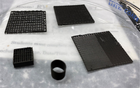
3D-printed Ni–PLGA samples placed in a glass Petri dish.
3. CVD Synthesis of 3D2G
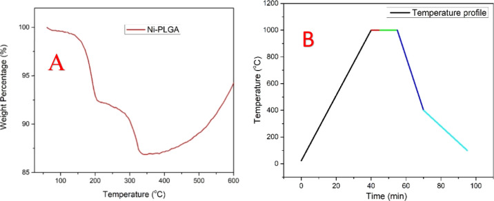
The presence of PLGA and DBP in the 3D-printed structures may interfere with the synthesis of graphene by hindering the exposure of nickel to the carbon precursor during CVD. For the complete removal of the polymers and to design the temperature profile for the CVD synthesis of 3D2G, understanding the thermal degradation of PLGA and DBP is important. A 4.36 mg (measured using Sartorius Me5) piece was cut from a 3D-printed nickel–PLGA structure and used for thermogravimetric analysis (TGA) conducted in air at a heating rate of 5 °C/min using a NETZSCH STA 409 PC. The thermogram shown in Figure 2a shows the reduction in the sample’s weight with an increase in temperature reaching the least weight percentage of 87% by 350 °C, which indicated a complete degradation of the polymers in the sample at this temperature. This thermal behavior in air is reasonable having in mind that PLGA is more thermally stable and degrades at around 350 °C while DBP disintegrates at about 200 °C.30,31 Any further increase in temperature resulted in a rise in weight due to the formation of nickel oxide (NiO) which confirmed the exposure of nickel to air and complete degradation of the polymers.32
Figure 2.
(a) TGA of 4.36 mg of the Ni–PLGA sample performed in air at a 5 °C/min heating rate. (b) Temperature profile used for the CVD synthesis of 3D2G.
Based on the thermal degradation data acquired from TGA, a similar temperature profile used in our previous works15,20 was employed for the CVD synthesis of 3D2G. An ET-1000 First Nano reactor was used for the CVD synthesis and the procedure was described elsewhere.15,20 In brief, the CVD synthesis was conducted in four steps. After loading the sample inside the reactor, it was heated from room temperature to 1000 °C in 40 min in the presence of argon (1000 sccm) and hydrogen (325 sccm) gas mixture. After reaching 1000 °C, the reactor was held at this temperature for 5 min to stabilize the thermal conditions by maintaining the same gaseous environment. Immediately after that, methane was introduced for 7 min at 25 sccm along with argon and hydrogen at the same temperature. Finally, an optimized cooling step was applied in the presence of argon and hydrogen at the same flow rates. The various steps of the CVD synthesis are illustrated using a colored temperature profile in Figure 2b.
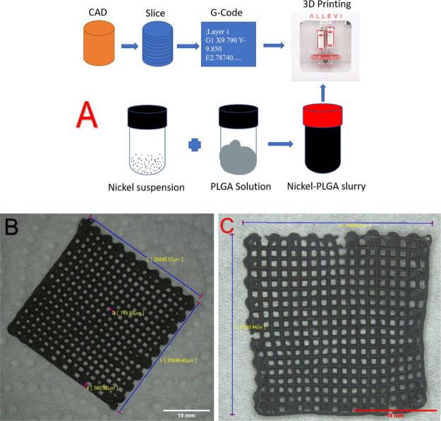
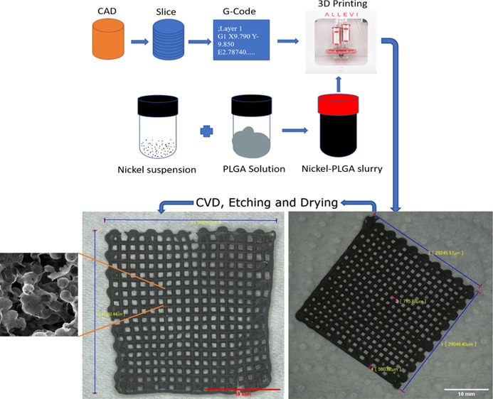
The resultant composite after CVD was transferred to a 15 M hydrochloric acid (HCl) bath to etch the nickel skeleton. Large samples were etched at temperatures in the range of 30–50 °C for 5–6 h and small samples with four layers or less were etched at room temperature overnight to preserve their sensitive structures. Finally, the etched samples were transferred to a DI water bath and rinsed for the removal of residual acid and salts, followed by an ethanol bath treatment for the removal of the residual water from the samples. On the other hand, large samples were dried using a Yamato DX 300 drying oven at 70 °C for 1.0–1.5 h, while the small samples were dried by lint-free KIMTECH Kimwipes for around 6 h. The resulting structure was 100% pristine graphene which was a highly porous freestanding state and is called here 3D2G. Figure 3 summarizes the entire process with the related steps involved in the synthesis of 3D2G. Figure 3a shows the 3D-printing steps in detail, Figure 3b is an image of a 3D-printed nickel–PLGA mesh before CVD, and Figure 3c is the resultant 3D2G obtained after the Ni etching and drying process.
Figure 3.
(a) Illustration of various steps involved in the 3D-printing process; (b) 3D-printed catalyst in a mesh shape with dimensions of 30 mm × 30 mm; and (c) resultant 3D2G with dimensions of around 22 mm × 23 mm, obtained after etching of the nickel catalyst and drying.
4. Results and Discussion
Various characterization techniques like scanning electron microscopy (SEM), energy-dispersive X-ray spectroscopy (EDX), SEM image analysis, microcomputed tomography (μCT), X-ray diffraction (XRD), Raman spectroscopy, Raman spectral analysis, TGA, electrical measurements, and cyclic voltammetry (CV) were used to expose various properties of 3D2G.
4.1. SEM and EDX
A high-resolution scanning electron microscope, Thermo Scientific Apreo, was used to study the morphology and to analyze the bulk porosity of 3D2G. For the conducted SEM imaging, a small piece was cut from the porous 3D2G sheet (8 layers, printed with a 23G needle), shown in Figure 3c, using a SS roller blade. The presence and retention of structural porosity in pristine 3D2G inherited from the 3D-printed catalyst can be seen in the top-view image, Figure 4a, while the cross-sectional image, Figure 4b, shows stacked 3D2G layers (bulk graphene) with good alignment.
Figure 4.
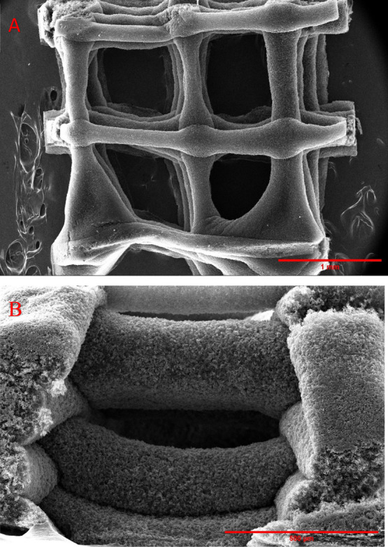
(a) Top view of the sample used for SEM analysis with a 1 mm scale bar; (b) side view of the sample used for SEM analysis with a 500 μm scale bar.
Furthermore, high-resolution SEM images of the bulk 3D2G surface, displayed in Figure 5a,b, showed a scaffold of interconnected hollow globules yielded due to the etching of the sintered nickel powder catalyst. Also, irregular pores resulted from the removal of the polymer can be observed in the same SEM images. These pores in the image in Figure 5b are highlighted in red color using FIJI (Fiji Is Just ImageJ) software, as shown in Figure 5c.
Figure 5.
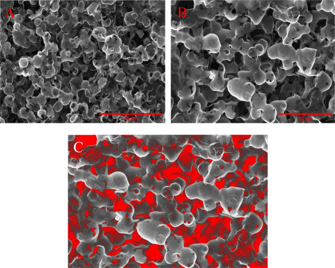
SEM images of bulk 3D2G at different magnifications. (a) 40 μm scale bar and (b) 20 μm scale bar. (c) Colored SEM image obtained by processing the image (b) using FIJI software highlighting irregular pores created due to polymer removal.
From Figure 4b, it was evident that the cut made using the SS roller blade created a shear on the sample resulting in bending of the overhanging struts in that area, hindering the cross-sectional microstructure details and related image analysis. To overcome this issue, samples with less than five layers were cut using a pulsed solid-state 532 nm laser milling system from Oxford Lasers. The samples were placed between two glass slides and were cut applying 80% power with 15 passes from one to the other side, followed by careful separation using tweezers. Figure 6a–d shows the cross-sectional view of the laser-cut samples at various magnifications, revealing the open porous structures created by laser postprocessing. Figure 6e displays the sample at an angle and highlights a line cut using 50% laser power which cuts the sample only halfway through.
Figure 6.
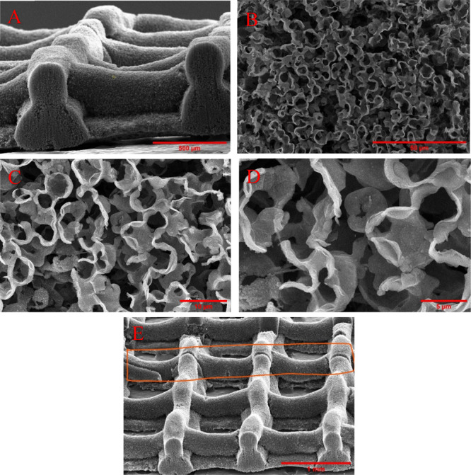
Cross-sectional view of the sample cut by a laser with a 532 nm wavelength at different magnifications. (a) 500 μm scale bar, (b) 50 μm scale bar, (c) 10 μm scale bar, and (d) 5 μm scale bar. (e) View of the sample at an angle showing a half-cut line created by the laser.
Due to the tight focus of the laser, layers close to the focal point (top layers) were cut easily. The beam diverged past the focal point and more laser power is needed to cut the bottom layers, resulting in melting and redeposition of material in the top layer, which can be noticed in the bottom left corner of Figure 6d.
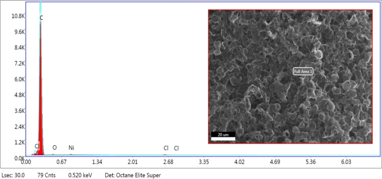
EDX data of 3D2G were dominated by carbon, as shown in Figure 7. A very small amount of oxygen, nickel, and chlorine was detected, which could be due to residual nickel salts left after hydrochloric acid etching of nickel.
Figure 7.
EDX analysis of 3D2G with an SEM image of the analyzed area.
4.2. TGA and XRD of 3D2G
A 2.51 mg (measured using Sartorius Me5) sample was cut from a 3D2G and used for TGA conducted in air at a heating rate of 5 °C/min by a NETZSCH STA 409 PC instrument. The obtained thermogravimetric data were plotted using OriginPro 9.0 and are displayed in Figure 8a.
Figure 8.
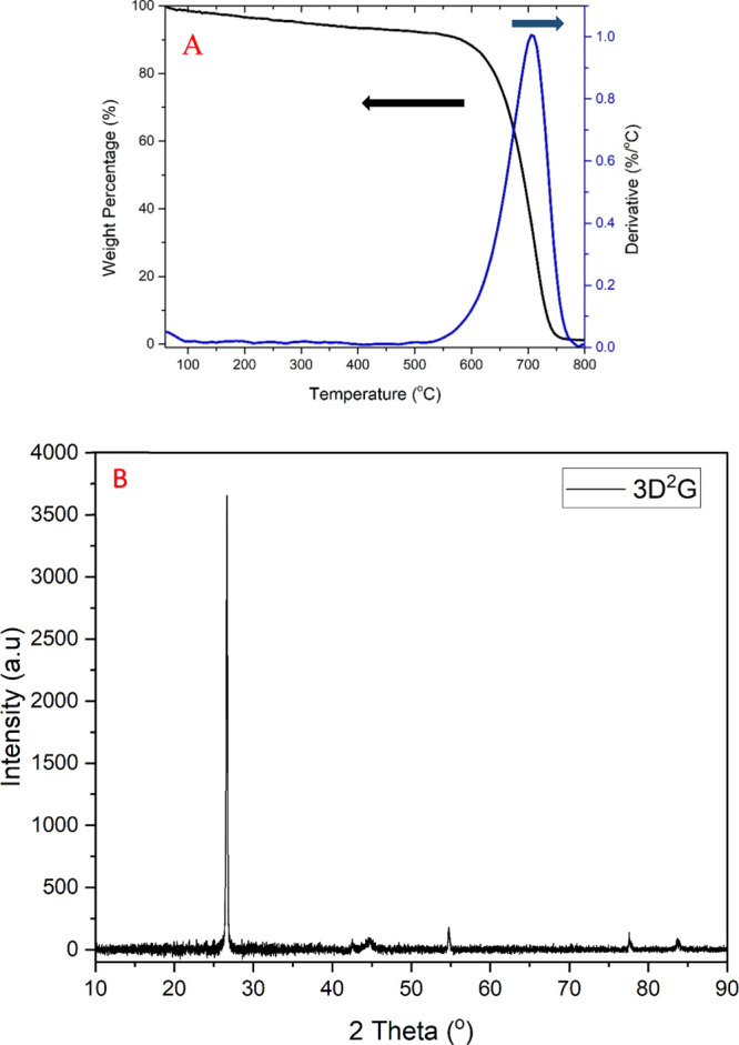
(a) TGA data of a 2.51 mg 3D2G sample heated in air at 5 °C/min; (b) XRD of pristine 3D2G.
In Figure 8a, the TGA curve is represented in black color, and its first derivative (DTG) is plotted as a blue curve. A large peak was observed between 550 and 780 °C, reaching a maximum of around 700 °C, illustrating the start and end of the oxidation and burning of crystalline carbon in the sample.15,33 No other peaks were observed except for a steady decrease in weight percentage with an increase in temperature. The TGA curve also interprets the stability of 3D2G at higher temperature considering only a loss of around 5% weight by 500 °C. In contrast, other 3D-printed graphene structures reported in the literature start disintegrating shortly above 150 °C due to the presence of the polymer/gel phases in their final constructions.27 After the complete burning of crystalline carbon, our sample reached an overall weight percentage of 0.9% at 800 °C, which may be related to residual nickel in the sample being converted to NiO.
A Rigaku SmartLab XRD system with a Cu Kα radiation source was used to study pristine 3D2G at room temperature, scanning within the 2θ range from 10 to 90°. Figure 8b shows an XRD spectrum of 3D2G. A large peak was observed at a 2θ value of 26.57° along with other common peaks characteristic of multilayered carbon materials. No shift of this peak was noticed, implying the absence of any doping with external elements or stress accumulation, thus corroborating the pristine nature of 3D2G. No nickel, nickel chloride, or NiO peaks were observed in the XRD spectra due to the limited sensitivity of this analytical technique. The presence of nickel products with a very low quantity (0.9 wt % as analyzed by TGA) is the reason for the absence of nickel peaks in the final XRD spectra.
4.3. SEM Image Analysis Using FIJI and MATLAB
The interconnected pores of 3D2G offer a favorable environment and functionality of this material for various advanced applications. The size of the structural pores of 3D2G is in the range of hundreds of microns, as shown in Figures 3, 4a, and 6e, and can be estimated using the scale option in FIJI. To find out the average pore size in the bulk sample, the high-resolution cross-sectional SEM images shown in Figure 6b–d were used. As the pore size is nonuniform as shown in Figures 5 and 6, measuring the individual pore size takes more time and may involve human error. For this reason, FIJI and MATLAB porosity modules34 were used. The high-resolution SEM image shown in Figure 6b was chosen as a sample for the image analysis.
FIJI was efficient in identifying and segmenting large pores; however, it failed to recognize small pores, which can be observed in Figure S4b (Supporting Information). For this reason, the same image shown in Figure 6b was used as a sample for porosity analysis employing an advanced MATLAB module. MATLAB performed better in identifying and segmenting pores that were processed and color-coded, as shown in Figure 9c. This procedure yielded an average pore size of around 6.5 μm.
Figure 9.
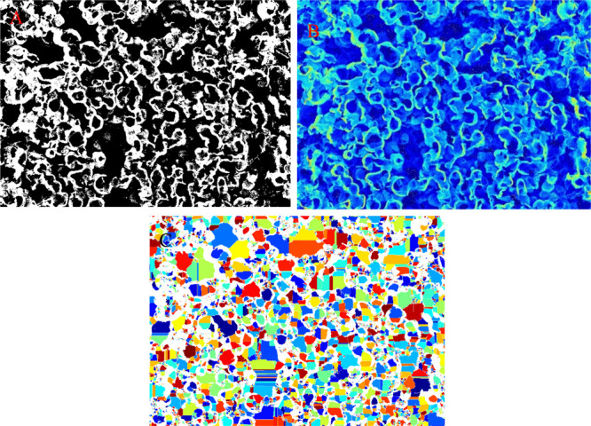
(a) Binary segmentation map, (b) depth map, and (c) pore segmentation maps of the SEM image shown in Figure 6b created using MATLAB analysis.
4.4. Micro X-ray-Computed Tomography
During CVD, the 3D-printed nickel–PLGA catalyst is exposed to 1000 °C for 13 min as discussed earlier. Optimal sintering of nickel powder in the structure is very crucial to reach the desired internal porosity (bulk) and to avoid structural failure of 3D2G. Understanding the sintering behavior plays a key role in obtaining the integrity and perfect stacking of the printed graphene struts (bulk graphene layers) in 3D2G. The latter is displayed in Figures 4b and 6a. Hence, forming the nickel–graphene composites in each layer (in-plane and perpendicular to the plane) and at the junctions between the struts was analyzed by X-ray-computed tomography (μCT) using a GE Phoenix Nanotom-M, Waygate Technologies. Various cylindrical and cuboid Ni–graphene structures were studied after CVD and the 3D scans of the same are displayed in Figure 10a,b, highlighting very good stacking of the layers in the zoomed-in view of the sintered structure shown in Figure 10c. The large structures were imaged at 130 kV source voltage, 100 μA source current (mode 0) using a tungsten-diamond target, and a 0.3 mm copper filter with a 500 ms exposure time at 9 μm isotropic voxel resolution. Data were collected from 1440 projections over 360° (0.25° steps) with three averaged images per rotation position.
Figure 10.
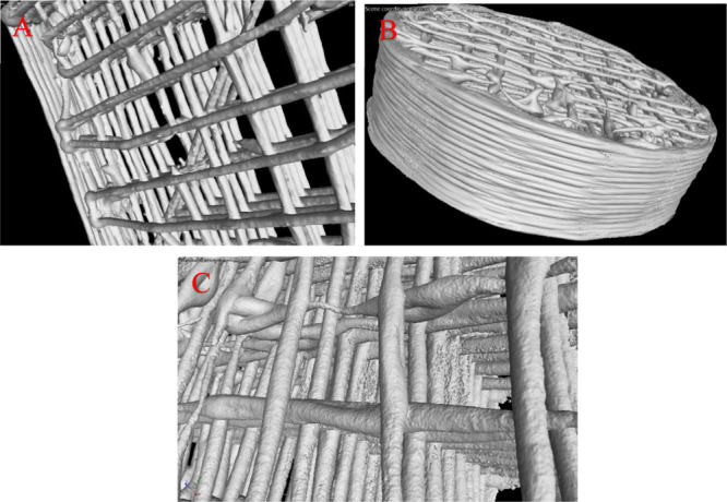
μCT scan of 3D-printed nickel–graphene after CVD. (a) Cuboid; (b) cylinder; and (c) zoomed-in image showing the stacking of the sintered layers.
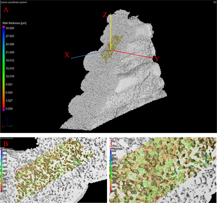
Though the scanned samples gave a good overview of the layer stacking, the low-resolution scans did not provide insights into the sintering of the nickel powder within the structure. To resolve this, a small piece was cut from an edge of the 3D-printed sample shown in Figure 10a with the length of the struts aligned along the X-axis, the Z-axis represented the direction of the height of the sample, and the Y-axis coincided with the other perpendicular direction. This sample was imaged at 130 kV source voltage, 55 μA source current (mode 2) using a tungsten-diamond target, and a 0.3 mm copper filter with a 500 ms exposure time at 0.83 μm isotropic voxel resolution. A total of 2160 projections were collected over 360° (0.17° steps) with two averaged images per rotation position.
The volume reconstructions were performed using Phoenix Datos software. The 3D scan of the sample with the coordinate axis is displayed in Figure 11a, highlighting the area used for high-resolution analysis. Zoomed-in images of the analyzed area are highlighted in Figure 11b,c.
Figure 11.
μCT scan of 3D-printed nickel–graphene after CVD. (a) Tested sample highlighting the area used for high-resolution analysis; (b,c) zoomed-in images of the analyzed area.
From images in Figure S5 of the Supporting Information, a complete sintering of the nickel catalyst particles in the form of a 3D metal scaffold can be observed, which offered a large Ni surface for exposure to the carbon precursor during the CVD process. Figure S6 shows μCT scans of the nickel–graphene composite sample in three different scan directions (X, Y, and Z). These scans are discussed in detail in Section S5 of the Supporting Information. In brief, the μCT scans in that section suggest a very good sintering of nickel inside each layer and between the layers, which is the reason behind the good structural integrity of 3D2G.
4.5. Raman Spectroscopy and Raman 2D Mapping
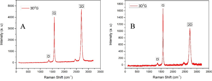
Raman spectroscopy emerged as an important nondestructive tool to study and evaluate nanostructured carbon materials. The three signature Raman peaks of graphene D, G, and 2D are frequently used to track the presence of doping,35 strain,36,37 and the number of layers within the graphene flakes.38,39 The presence of the D peak can be related to the breathing modes of sp2 carbon atoms in the rings. It represents the defects or disorder in the structure and helps in differentiating graphene from its derivatives. The G peak exemplifies the stretching of the in-plane C–C bonds, while the 2D peak is the overtone of the D peak.15,40,41 A 514 nm argon-ion laser having a 1 μm2 spot diameter and an output of 8 mW of power was used to study the Raman spectra of 3D2G employing a Renishaw inVia Raman spectroscopy instrument. Various random spots on the samples were probed, and the spectra were plotted using OriginPro 9.0. The obtained spectra are shown in Figure 12, highlighting the signature D, G, and 2D peaks of graphene at two different points.
Figure 12.
(a,b) Raman spectrum of 3D2G at two distinct points.
From the Raman data obtained, a very small D peak was observed in all the spectra, representing the least amount of surface defects in the samples.42 Furthermore, a wide range of 2D and G peak intensities were observed, as shown in Figure 12. The intensity ratio of G and 2D peaks [I(G)/I(2D)] can help in estimating the number of layers present within the probed graphene flake.38 A higher intensity ratio is expected and observed considering the relatively high solubility of carbon in nickel and the polycrystalline nature of the nickel powder used, indicating the presence of multilayer graphene.43 If only the I(G)/I(2D) intensity ratio is considered, Figure 12a shows a probed point with fewer layers than the point whose spectrum is shown in Figure 12b.38 Furthermore, the estimation of the number of layers using the intensity ratio cannot apply when more than one variety of graphene layer stacking is present. CVD-grown graphene on polycrystalline nickel may yield multilayer graphene with Bernal stacking (ABAB...) or rotationally faulted layers and a combination of these two. The I(G)/I(2D) intensity ratios may mislead the number of layer estimations in the presence of layer rotation.44,45 The intensity ratio along with the 2D peak full width at half-maximum (FWHM) may help in developing a better understanding of the 3D2G Raman spectrum. The spectrum with I(G)/I(2D) in the range 0.2–0.4 and a 2D fwhm in the range of 26–38 cm–1 is considered as monolayer graphene. The spectrum with I(G)/I(2D) in the range of 0.45–1.4 and a 2D FWHM ranging from 39 to 70 cm–1 is regarded as bilayer graphene, and the spectrum with I(G)/I(2D) > 1.4 and 2D FWHM > 70 cm–1 is viewed as few or multilayer graphene.39
It is obvious from the above discussion that representing Raman spectra of the CVD-grown 3D2G on nickel using a single probing point is not comprehensive considering the possible variations in the intensities of the respective peaks from point to point. For this reason, the so-called 2D Raman spectroscopy can provide more comprehensive data. Such a Raman spectral analysis (mapping) enables an aerial analysis with thousands of points within the studied area. The obtained Raman maps combined with data analysis and statistical approaches can better interpret the Raman spectrum of 3D2G.
In this study, a 532 nm laser was used for confocal Raman mapping enabled by a HORIBA LabRam Aramis instrument. A 2D area of 100 × 100 μm2 on a 1 cm × 1.2 cm rectangular 3D2G-printed sample was used for the spectral analysis at 50x magnification. The sample was printed using a 410 μm straight SS blunt needle with a rectilinear infill and an infill density of 30. Each analyzed area consisted of 10,201 spectra data points. The spectral analysis was carried using two different samples representing two stages of the sample preparation. The first one was the nickel–graphene composite obtained after CVD. The second sample was pristine 3D2G obtained after acid etching of the nickel catalyst. All the maps were cleaned, and the peaks were fitted using the GaussLor function (a convolution of Gaussian and Lorentzian functions) in LabSpec 6. Then, the data were exported as a text file, and histograms were plotted in Excel. The individual spectra and 2D peak analysis were done in OriginPro 9.0.
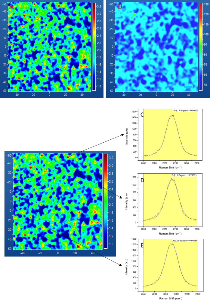
Figure 13a,b shows the distribution of the I(G)/I(2D) ratio and 2D peak FWHM, respectively, across the analyzed area on 3D2G with the obtained mean values of 1.8 and 66.6 cm–1 for the intensity ratio and 2D peak FWHM maps. From these figures, it is obvious that a wide range of intensity ratios exist, dominated by high I(G)/I(2D) ratios (>1.4) and 2D peak fwhms (>55 cm–1), indicating the presence of multilayer graphene in the 3D2G. Spectra with high-intensity ratios (>2.3) revealed a graphite-like very short 2D peak and a tall G peak with a 2D peak FWHM below 70 cm–1 without a shoulder, which is not typical for a graphite Raman spectrum. For further analysis, three random points representing three different intensity ratios (>2.2) were chosen. The spectral data were exported, and the 2D peak was fitted using a Voigt profile (convolution of Gaussian and Lorentzian functions)46 in OriginPro 9.0. The 2D peak profile shown in Figure 13c–e represents the spectra within the red, yellow, and green areas of the intensity ratio map. In all these points, the Voigt profile fits perfectly with the 2D peak profile. The obtained adj. R2 value was close to 1, resembling a nongraphitic 2D peak without a shoulder.47 The observed tall G peak with a small nongraphitic 2D peak may represent rotation in multilayer CVD graphene synthesized on the nickel catalyst, as reported earlier.43,44,48,49
Figure 13.
(a) I(G)/I(2D) ratio map of 3D2G with a 10 μm scale bar; (b) 2D peak fwhm of 3D2G with a 10 μm scale bar; (c) 2D peak Voigt peak fit in the red area; (d) 2D peak Voigt peak fit in the yellow area; and (e) 2D peak Voigt peak fit in the green area. (c–e) 2D peak from the image shown in (a).
The 2D Raman data of the nickel–graphene composite are shown in Figure S7a,b in the Supporting Information. A comparison of the intensity ratio I(G)/I(2D) and 2D peak FWHM of 3D2G and the nickel–graphene composite is shown as bar graphs in Figure S6c,d.
4.6. Electrochemical and Electrical Characterization
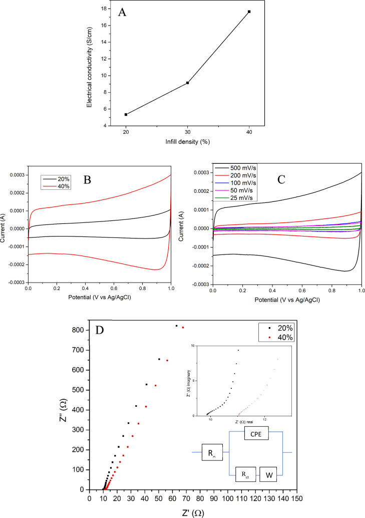
Three different 3D2G samples with 1.7 mm × 1.2 mm × 0.5 mm dimensions were prepared to measure their electrical conductivity. The samples were 3D-printed using a 430-μm needle, yielding rectilinear infill with an infill density of 20, 30, and 40%, respectively. SEM images of the 30% infill sample have been already shown in Figure 6a–d. A van der Pauw (Keysight Technologies 34460A) 4-point instrument was used to analyze the electrical conductivity of the samples. All corners of the samples were coated with silver paste, and the four terminals of the probe were slightly compressed on the silver-coated spots of the specimens for measurement. The sample with 40% infill showed the highest electrical conductivity of 17.66 S/cm and the sample with 20% infill exhibited the least electrical conductivity of 5.35 S/cm, as displayed in Figure 14a. This trend was expected since the samples with lower infill had larger pores with less material in them. Here, the amount of material and the pore size have a synergetic effect on the electrical conductivity. The 20, 30, and 40% infill samples showed an electrical conductivity of ≈2.43, ≈2.8, and ≈3.4 S/cm mg, respectively, after normalizing by mass. The higher conductivity of the 40% sample after normalizing is due to the presence of smaller structural pores when compared to those with 20 and 30% infill.
Figure 14.
(a) Electrical conductivity of 3D2G with various infill densities; (b) CV curves of 3D2G with 20 and 40% infill at a 500 mV/s scan rate; (c) CV curves of 3D2G with 40% infill at various scan rates; and (d) Nyquist plot for 20 and 40% infill samples. The insets in (d) show the high-frequency range of the EIS curve (top) and the equivalent circuit diagram (bottom).
Furthermore, the electrochemical performance of 3D2G was analyzed using a Gamry Interface 1000 in a three-electrode arrangement where a platinum wire was used as the counter electrode and an Ag/AgCl electrode was employed as the reference electrode in a 1 M sodium sulfate (Na2SO4) electrolyte. The voltage window was set from 0.0 to 1.0 V, and the measurements were conducted at various scan rates of 25, 50, 100, 200, and 500 mV/s at room temperature. The obtained curves showed a typical electric double-layer capacitor behavior, as shown in the resultant CV graphs in Figure 14b,c. Figure 14b shows a comparison of CV curves obtained from two samples with 20% infill and 40% infill density at a scan rate of 500 mV/s. Figure 14c shows the CV curves of the sample with 40% infill at various scan rates. A relative comparison of the areas within the curves in Figure 14b revealed that the capacitance of the 40% infill sample was around four times the capacitance of the 20% infill sample at a 500 mV/s scan rate. This can be attributed to more surface areas created due to the higher mass present in the 40% infill sample.
The results of the electrochemical impedance spectroscopy test over a frequency range of 105 to 10–2 Hz at an amplitude of 10 mV are plotted in Figure 14d, with an inset showing the high-frequency region (top). It is clear from this inset that an unnoticeable semicircle was present with a diameter of around 2–3 Ω for both samples (20 and 40% infill), showing a low interfacial resistance between the electrolyte and the electrode. This was represented by Rct as shown in the equivalent circuit diagram in the inset of Figure 14d.
5. Conclusions
A comprehensive procedure to synthesize 3D2G is reported along with its material characterization. Initial data on the electrical and electrochemical properties of 3D2G have been presented. The conducted detailed Raman study on the quality of 3D2G revealed its good quality and multilayered nature. According to the DTA data, this material is of high purity and thermally very stable. The synthesized 3D2G can be customized into any shape or size according to the application requirements without losing its quality and structural integrity. By simply changing the printing design, various properties such as porosity, electrical conductivity, and capacitance can be tuned to fit the desired application. The obtained binder-free 3D2G appears to be a good candidate for application as a material for gas sensors, energy storage electrodes, gas filters, thermal electric components,50 EMI shielding,51 and other thermally and electrically related applications where surface area, porosity, electrical conductivity, and structural design matter.
Acknowledgments
This research study was partially supported by the National Institute for Occupational Safety and Health through the Pilot Research Project Training Program of the University of Cincinnati Education and Research Center Grant #T42OH008432. The GE Phoenix Nanotom-180 M X-Ray CT instrument used in this study was acquired via NSF MRI-R2 award #0959511. One of the authors (V.K.R.K.) would like to thank the Graduate Student Government (GSG) at the University of Cincinnati for the Research Fellowship and also the Department of Engineering Education at the University of Cincinnati for the financial support via a Graduate Assistantship. The authors would like to thank Dr. Je-Hyeong Bahk and Yu Zhang at the University of Cincinnati for their help with the electrical conductivity measurements. The authors would also like to acknowledge the help of Dr. Melodie Fickenscher at the University of Cincinnati Advanced Materials Characterization Center (AMCC).
Supporting Information Available
The Supporting Information is available free of charge at https://pubs.acs.org/doi/10.1021/acsomega.1c04072.
Screenshot of the Tinkercad work environment with a solid cube (20 mm × 20 mm × 20 mm), a cuboid (20 mm × 20 mm × 1.2 mm), and a cylinder of a diameter of 20 mm and height of 20 mm; screenshot showing the complex structure generated after processing the solid cylinder STL in the Slic3r work environment; illustration of a simple square-shaped movement of the print head in CAMotics; screenshot of the respective G-code to enable the movement shown in Figure 3a; threshold map of the SEM image shown in Figure 6b created using FIJI; pore separation map with pore outlines extracted and numbered by FIJI; high-resolution SEM images of the nickel scaffold at different magnifications as follows: 1 mm scale bar, 50 μm scale bar, and 3 μm scale bar; analyzed area at three different × coordinates as follows: 400 μm at 100 μm scale bar, 500 μm at 100 μm scale bar, and 600 μm at 100 μm scale bar; analyzed area at two different interfaces between the struts in the Z direction on the left with the respective X-axis images on the right for the top junction at 50 μm scale bar and bottom junction at μm scale bar; analyzed area at three different Y coordinates as follows: 20 μm at 150 μm scale bar, 40 μm at 150 μm scale bar, and 60 μm at 150 μm scale bar; I(G)/I(2D) ratio map of 3D2G with 10 μm scale bar; 2D peak fwhm of 3D2G with 10 μm scale bar; histogram comparing the intensity ratio of 3D2G and the nickel–graphene composite; and histogram comparing the 2D peak fwhm of 3D2G and the nickel–graphene composite (PDF)
The authors declare no competing financial interest.
Supplementary Material
References
- Nika D. L.; Balandin A. A. Thermal Transport in Graphene, Few-Layer Graphene and Graphene Nanoribbons. Lect. Notes Phys. 2016, 921, 339–363. 10.1007/978-3-319-29261-8_9. [DOI] [Google Scholar]
- Calizo I.; Balandin A. A.; Bao W.; Miao F.; Lau C. N. Temperature Dependence of the Raman Spectra of Graphene and Graphene Multilayers. Nano Lett. 2007, 7, 2645–2649. 10.1021/nl071033g. [DOI] [PubMed] [Google Scholar]
- Balandin A. A.; Ghosh S.; Bao W.; Calizo I.; Teweldebrhan D.; Miao F.; Lau C. N. Superior Thermal Conductivity of Single-Layer Graphene. Nano Lett. 2008, 8, 902–907. 10.1021/nl0731872. [DOI] [PubMed] [Google Scholar]
- Balandin A. A. Thermal properties of graphene and nanostructured carbon materials. Nat. Mater. 2011, 10, 569–581. 10.1038/nmat3064. [DOI] [PubMed] [Google Scholar]
- Abhinav C.; Vamsi Krishna Reddy K.; Goutham Raju G.; Subramanyam K. Experimental Investigation of Graphene coated Al cuboid crammed with PCM’s for Efficient Thermal Energy Storage and Conversion. Int. Res. J. Eng. Technol. 2017, 4, 396–402. [Google Scholar]
- Vamsi Krishna Reddy K.; Abhinav C. Brief Review on Thermal Properties of Graphene-Aluminium Metal Matrix Composites. Int. J. Adv. Eng. Nano Technol. 2016, 3, 2347–6389. [Google Scholar]
- Wang H.; Kurata K.; Fukunaga T.; Ago H.; Takamatsu H.; Zhang X.; Ikuta T.; Takahashi K.; Nishiyama T.; Takata Y. Simultaneous measurement of electrical and thermal conductivities of suspended monolayer graphene. J. Appl. Phys. 2016, 119, 244306. 10.1063/1.4954677. [DOI] [Google Scholar]
- Yuan W.; Shi G. Graphene-based gas sensors. J. Mater. Chem. A 2013, 1, 10078–10091. 10.1039/c3ta11774j. [DOI] [Google Scholar]
- Mortazavi Zanjani S. M.; Holt M.; Sadeghi M. M.; Rahimi S.; Akinwande D. 3D integrated monolayer graphene–Si CMOS RF gas sensor platform. npj 2D Mater. Appl. 2017, 1, 36. 10.1038/s41699-017-0036-0. [DOI] [Google Scholar]
- Wei D.; Haque S.; Andrew P.; Kivioja J.; Ryhänen T.; Pesquera A.; Centeno A.; Alonso B.; Chuvilin A.; Zurutuza A. Ultrathin rechargeable all-solid-state batteries based on monolayer graphene. J. Mater. Chem. A 2013, 1, 3177–3181. 10.1039/c3ta01183f. [DOI] [Google Scholar]
- Ollik K.; Lieder M. Review of the application of graphene-based coatings as anticorrosion layers. Coatings 2020, 10, 883. 10.3390/coatings10090883. [DOI] [Google Scholar]
- Novoselov K. S.; Geim A. K.; Morozov S. V.; Jiang D.; Zhang Y.; Dubonos S. V.; Grigorieva I. V.; Firsov A. A. Electric field in atomically thin carbon films. Science 2004, 306, 666–669. 10.1126/science.1102896. [DOI] [PubMed] [Google Scholar]
- Kalita G.; Tanemura M.. Fundamentals of Chemical Vapor Deposited Graphene and Emerging Applications. Graphene Materials-Advanced Applications, IntechOpen, 2017. [Google Scholar]
- Papon R.; Pierlot C.; Sharma S.; Shinde S. M.; Kalita G.; Tanemura M. Optimization of CVD parameters for graphene synthesis through design of experiments. Phys. Status Solidi B 2017, 254, 1600629. 10.1002/pssb.201600629. [DOI] [Google Scholar]
- DeArmond D.; Zhang L.; Malik R.; Vamsi Krishna Reddy K.; Alvarez N. T.; Haase M. R.; Hsieh Y.-Y.; Kanakaraj S. N.; Oslin N.; Brunemann J.; Daum J.; Shanov V. Scalable CVD synthesis of three-dimensional graphene from cast catalyst. Mater. Sci. Eng., B 2020, 254, 114510. 10.1016/j.mseb.2020.114510. [DOI] [Google Scholar]
- Lin L.; Deng B.; Sun J.; Peng H.; Liu Z. Bridging the Gap between Reality and Ideal in Chemical Vapor Deposition Growth of Graphene. Chem. Rev. 2018, 118, 9281–9343. 10.1021/acs.chemrev.8b00325. [DOI] [PubMed] [Google Scholar]
- Polsen E. S.; McNerny D. Q.; Viswanath B.; Pattinson S. W.; John Hart A. High-speed roll-to-roll manufacturing of graphene using a concentric tube CVD reactor. Sci. Rep. 2015, 5, 10257. 10.1038/srep10257. [DOI] [PMC free article] [PubMed] [Google Scholar]
- Vlassiouk I.; Regmi M.; Fulvio P.; Dai S.; Datskos P.; Eres G.; Smirnov S. Role of hydrogen in chemical vapor deposition growth of large single-crystal graphene. ACS Nano 2011, 5, 6069–6076. 10.1021/nn201978y. [DOI] [PubMed] [Google Scholar]
- Yavari F.; Chen Z.; Thomas A. V.; Ren W.; Cheng H. M.; Koratkar N. High sensitivity gas detection using a macroscopic three-dimensional graphene foam network. Sci. Rep. 2011, 1, 166. 10.1038/srep00166. [DOI] [PMC free article] [PubMed] [Google Scholar]
- Zhang L.; DeArmond D.; Alvarez N. T.; Zhao D.; Wang T.; Hou G.; Malik R.; Heineman W. R.; Shanov V. Beyond graphene foam, a new form of three-dimensional graphene for supercapacitor electrodes. J. Mater. Chem. A 2016, 4, 1876–1886. 10.1039/c5ta10031c. [DOI] [Google Scholar]
- Ping Y.; Gong Y.; Fu Q.; Pan C. Preparation of three-dimensional graphene foam for high performance supercapacitors. Prog. Nat. Sci. Mater. Int. 2017, 27, 177–181. 10.1016/j.pnsc.2017.03.005. [DOI] [Google Scholar]
- Sha J.; Li Y.; Villegas Salvatierra R.; Wang T.; Dong P.; Ji Y.; Lee S.-K.; Zhang C.; Zhang J.; Smith R. H.; Ajayan P. M.; Lou J.; Zhao N.; Tour J. M. Three-Dimensional Printed Graphene Foams. ACS Nano 2017, 11, 6860–6867. 10.1021/acsnano.7b01987. [DOI] [PubMed] [Google Scholar]
- Yang Y.; Gu D.; Dai D.; Ma C. Laser energy absorption behavior of powder particles using ray tracing method during selective laser melting additive manufacturing of aluminum alloy. Mater. Des. 2018, 143, 12–19. 10.1016/j.matdes.2018.01.043. [DOI] [Google Scholar]
- Lin J.; Peng Z.; Liu Y.; Zepeda F. R.; Ye R.; Samuel E. L. G.; Yacaman M. J.; Yakobson B. I.; Tour J. M. Laser-induced porous graphene films from commercial polymers. Nat. Commun. 2014, 5, 5714. 10.1038/ncomms6714. [DOI] [PMC free article] [PubMed] [Google Scholar]
- Luong D. X.; Subramanian A. K.; Silva G. A. L.; Yoon J.; Cofer S.; Yang K.; Owuor P. S.; Wang T.; Wang Z.; Lou J.; Ajayan P. M.; Tour J. M. Laminated Object Manufacturing of 3D-Printed Laser-Induced Graphene Foams. Adv. Mater. 2018, 30, 1707416. 10.1002/adma.201707416. [DOI] [PubMed] [Google Scholar]
- Zhang Q.; Zhang F.; Medarametla S. P.; Li H.; Zhou C.; Lin D. 3D Printing of Graphene Aerogels. Small 2016, 12, 1702–1708. 10.1002/smll.201503524. [DOI] [PubMed] [Google Scholar]
- Jakus A. E.; Secor E. B.; Rutz A. L.; Jordan S. W.; Hersam M. C.; Shah R. N. Three-dimensional printing of high-content graphene scaffolds for electronic and biomedical applications. ACS Nano 2015, 9, 4636–4648. 10.1021/acsnano.5b01179. [DOI] [PubMed] [Google Scholar]
- Taylor S. L.; Jakus A. E.; Shah R. N.; Dunand D. C. Iron and Nickel Cellular Structures by Sintering of 3D-Printed Oxide or Metallic Particle Inks . Adv. Eng. Mater. 2017, 19, 1600365. 10.1002/adem.201600365. [DOI] [Google Scholar]
- Jakus A. E.; Taylor S. L.; Geisendorfer N. R.; Dunand D. C.; Shah R. N. Metallic Architectures from 3D-Printed Powder-Based Liquid Inks. Adv. Funct. Mater. 2015, 25, 6985–6995. 10.1002/adfm.201503921. [DOI] [Google Scholar]
- Wei R.; Huang S.; Wang Z.; Wang C.; Zhou T.; He J.; Yuen R.; Wang J. Effect of plasticizer dibutyl phthalate on the thermal decomposition of nitrocellulose. J. Therm. Anal. Calorim. 2018, 134, 953–969. 10.1007/s10973-018-7521-3. [DOI] [Google Scholar]
- Ayyoob M.; Kim Y. Effect of Chemical Composition Variant and Oxygen Plasma Treatments on the Wettability of PLGA Thin Films, Synthesized by Direct Copolycondensation. Polymers 2018, 10, 1132. 10.3390/polym10101132. [DOI] [PMC free article] [PubMed] [Google Scholar]
- Hansen G.; Næss E.; Kristjansson K. Sintered Nickel Powder Wicks for Flat Vertical Heat Pipes. Energies 2015, 8, 2337–2357. 10.3390/en8042337. [DOI] [Google Scholar]
- Chen H. S.; Kortan A. R.; Haddon R. C.; Kaplan M. L.; Chen C. H.; Mujsce A. M.; Chou H.; Fleming D. A. Reactivity of C60 in pure oxygen. Appl. Phys. Lett. 1991, 59, 2956–2958. 10.1063/1.105810. [DOI] [Google Scholar]
- Rabbani A.; Salehi S. Dynamic modeling of the formation damage and mud cake deposition using filtration theories coupled with SEM image processing. J. Nat. Gas. Sci. Eng. 2017, 42, 157–168. 10.1016/j.jngse.2017.02.047. [DOI] [Google Scholar]
- Dasgupta K.; Khosravifar M.; Sawant S.; Adusei P. K.; Kanakaraj S. N.; Kasik J.; Shanov V. Nitrogen-Doped Flower-Like Hybrid Structure Based on Three-Dimensional Graphene. C—J. Carbon Res. 2020, 6, 40. 10.3390/c6020040. [DOI] [Google Scholar]
- Wang Y.; Panzik J. E.; Kiefer B.; Lee K. K. M. Crystal structure of graphite under room-temperature compression and decompression. Sci. Rep. 2012, 2, 520. 10.1038/srep00520. [DOI] [PMC free article] [PubMed] [Google Scholar]
- Bissett M. A.; Tsuji M.; Ago H. Strain engineering the properties of graphene and other two-dimensional crystals. Phys. Chem. Chem. Phys. 2014, 16, 11124. 10.1039/c3cp55443k. [DOI] [PubMed] [Google Scholar]
- Das A.; Chakraborty B.; Sood A. K. Raman spectroscopy of graphene on different substrates and influence of defects. Bull. Mater. Sci. 2008, 31, 579–584. 10.1007/s12034-008-0090-5. [DOI] [Google Scholar]
- Madito M. J.; Matshoba K. S.; Ochai-Ejeh F. U.; Mongwaketsi N.; Mtshali C. B.; Fabiane M.; Manyala N. Nickel-copper graphene foam prepared by atmospheric pressure chemical vapour deposition for supercapacitor applications. Surf. Coat. Technol. 2020, 383, 125230. 10.1016/j.surfcoat.2019.125230. [DOI] [Google Scholar]
- Fang Y.; Hsieh Y.-Y.; Khosravifar M.; Johnson K.; Kwasi Adusei P.; Kanakaraj S. N.; Preisler S.; Zhang G.; Shanov V. Lithiophilic current collector based on nitrogen doped carbon nanotubes and three-dimensional graphene for long-life lithium metal batteries. Mater. Sci. Eng., B 2021, 267, 115067. 10.1016/j.mseb.2021.115067. [DOI] [Google Scholar]
- Ferrari A. C. Raman spectroscopy of graphene and graphite: Disorder, electron-phonon coupling, doping and nonadiabatic effects. Solid State Commun. 2007, 143, 47–57. 10.1016/j.ssc.2007.03.052. [DOI] [Google Scholar]
- Ni Z.; Wang Y.; Yu T.; Shen Z. Raman spectroscopy and imaging of graphene. Nano Res. 2010, 1, 273–291. 10.1007/s12274-008-8036-1. [DOI] [Google Scholar]
- Lavin-Lopez M. P.; Valverde J. L.; Ruiz-Enrique M. I.; Sanchez-Silva L.; Romero A. Thickness control of graphene deposited over polycrystalline nickel. New J. Chem. 2015, 39, 4414. 10.1039/c5nj00073d. [DOI] [Google Scholar]
- Niilisk A.; Kozlova J.; Alles H.; Aarik J.; Sammelselg V. Raman characterization of stacking in multi-layer graphene grown on Ni. Carbon 2016, 98, 658–665. 10.1016/j.carbon.2015.11.050. [DOI] [Google Scholar]
- Kato H.; Itagaki N.; Im H. J. Growth and Raman spectroscopy of thickness-controlled rotationally faulted multilayer graphene. Carbon 2019, 141, 76–82. 10.1016/j.carbon.2018.09.017. [DOI] [Google Scholar]
- Wertheim G. K.; Butler M. A.; West K. W.; Buchanan D. N. E. Determination of the Gaussian and Lorentzian content of experimental line shapes. Rev. Sci. Instrum. 1974, 45, 1369–1371. 10.1063/1.1686503. [DOI] [Google Scholar]
- Roscher S.; Hoffmann R.; Ambacher O. Determination of the graphene-graphite ratio of graphene powder by Raman 2D band symmetry analysis. Anal. Methods 2019, 11, 1224. 10.1039/c8ay02619j. [DOI] [Google Scholar]
- Ta H. Q.; Perello D. J.; Duong D. L.; Han G. H.; Gorantla S.; Nguyen V. L.; Bachmatiuk A.; Rotkin S. V.; Lee Y. H.; Rümmeli M. H. Stranski-Krastanov and Volmer-Weber CVD Growth Regimes to Control the Stacking Order in Bilayer Graphene. Nano Lett. 2016, 16, 6403–6410. 10.1021/acs.nanolett.6b02826. [DOI] [PubMed] [Google Scholar]
- No Y.-S.; Choi H. K.; Kim J.-S.; Kim H.; Yu Y.-J.; Choi C.-G.; Choi J. S. Layer number identification of CVD-grown multilayer graphene using Si peak analysis. Sci. Rep. 2018, 8, 571. 10.1038/s41598-017-19084-1. [DOI] [PMC free article] [PubMed] [Google Scholar]
- Hsieh Y.-Y.; Zhang Y.; Zhang L.; Fang Y.; Kanakaraaj S. N.; Bahk J.-H.; Shanov V. High thermoelectric power-factor composites based on flexible three-dimensional graphene and polyaniline. Nanoscale 2019, 11, 6552–6560. 10.1039/c8nr10537e. [DOI] [PubMed] [Google Scholar]
- Zhang L.; Alvarez N. T.; Zhang M.; Haase M.; Malik R.; Mast D.; Shanov V. Preparation and characterization of graphene paper for electromagnetic interference shielding. Carbon 2015, 82, 353–359. 10.1016/j.carbon.2014.10.080. [DOI] [Google Scholar]
Associated Data
This section collects any data citations, data availability statements, or supplementary materials included in this article.


