

Abstract

Strain engineering can effectively improve the energy band degeneracy of two-dimensional transition metal dichalcogenides so that they exhibit good thermoelectric properties under strain. In this work, we have studied the phonon, electronic, thermal, and thermoelectric properties of 1T-phase monolayer HfS2 with biaxial strain based on first-principles calculations combined with Boltzmann equations. At 0% strain, the results show that the lattice thermal conductivity of monolayer HfS2 is 5.01 W m–1 K–1 and the electronic thermal conductivities of n-type and p-type doped monolayer HfS2 are 2.94 and 0.39 W m–1 K–1, respectively, when the doping concentration is around 5 × 1012 cm–2. The power factors of the n-type and p-type doped monolayer HfS2 are different, 29.4 and 1.6 mW mK–2, respectively. Finally, the maximum ZT value of the n-type monolayer HfS2 is 1.09, which is higher than 0.09 of the p-type monolayer HfS2. Under biaxial strain, for n-type HfS2, the lattice thermal conductivity, the electronic thermal conductivity, and the power factor are 1.55 W m–1 K–1, 1.44 W m–1 K–1, and 22.9 mW mK–2 at 6% strain, respectively. Based on the above factor, the ZT value reaches its maximum of 2.29 at 6% strain. For p-type HfS2, the lattice thermal conductivity and the electronic thermal conductivity are 1.12 and 1.53 W m–1 K–1 at 7% strain, respectively. Moreover, the power factor is greatly improved to 29.5 mW mK–2. Finally, the maximum ZT value of the p-type monolayer HfS2 is 3.35 at 7% strain. It is obvious that strain can greatly improve the thermoelectric performance of monolayer HfS2, especially for p-type HfS2. We hope that the research results can provide data references for future experimental exploration.
1. Introduction
In recent decades, as the energy crisis and environmental problems have become increasingly serious, researchers have begun to turn their attention to the development of high-efficiency energy.1−3 Thermoelectric materials have great potential in waste-heat recovery, reduce greenhouse gas emissions, and provide cleaner forms of energy.4 Thermoelectric devices not only have high application potential in aerospace components and household devices but can also be used in current integrated circuits to solve the problem of chip heat.5−7 Thermoelectric material is a kind of functional material that can directly convert thermal energy into electrical energy by carrier movement in solids.8,9 The performance of thermoelectric material is characterized by the dimensionless figure of merit, ZT = S2σT/κ = S2σT/(κe + κl), where S is the Seebeck coefficient, σ is the electronic conductivity, T is the temperature, and κ is the thermal conductivity including both the electronic contribution (κe) and the lattice thermal conductivity (κl).10 At present, the problem that hinders the large-scale application of thermoelectric materials is low thermoelectric conversion efficiency (low ZT value). However, it is very challenging to find suitable materials with large ZT since the transport coefficients (S, σ, κ) are interdependent quantities. Researchers found that band engineering,11−13 nanostructural engineering,14 and two-dimensional engineering15 can help enhance the Seebeck coefficient and reduce the thermal conductivity, thereby effectively improving the thermoelectric properties of materials.
It has been discovered that various two-dimensional (2D) materials have higher thermoelectric ZT and also can be widely used in practical applications. Thus, 2D materials have attracted much attention due to their unique properties.11,16−18 The main 2D thermoelectric materials are Group IVA–VIA compounds, black phosphorus (BP), nitrides, transition metal dichalcogenides (TMDCs), MXenes, and Xenes.19−22 Among the various 2D materials, ZT can be effectively improved by selecting structural materials with lower thermal conductivity. For example, metal-shrouded semiconductor Tl2O (group space R3̅m) with a 1T structure has good thermoelectric properties due to its low thermal conductivity.23 Likewise, TMDCs have also attracted much attention due to their relatively high electrical conductivity and relatively low thermal conductivity.16,24 2D TMDCs are divided into two kinds of crystal structures according to the arrangement of the atoms and the structures: trigonal prismatic (hexagonal, 2H-MoS2 type) and octahedral (tetragonal, 1T-CdI2 type). MoS2 and WS2 are typical TMDCs with a 2H-MoS2 structure. Theoretical studies25,26 indicated that the maximum ZT value of monolayer MoS2 (monolayer WS2) is 0.58 (0.067) at room temperature, which is mainly due to the high lattice thermal conductivity. Compared with the 2H-MoS2 structure, the TMDC MX2 (M = Zr, Hf; X = S, Se) with the 1T-CdI2 structure has a much lower lattice thermal conductivity and a higher ZT value at room temperature.27 For example, Bera et al. calculated that the ZT of monolayer HfS2 (group space P3̅m1) is 0.60,28 and Singh et al. reported that the maximum ZT is 0.96.29 Özbal et al. found that the ZT of TMDC HfS2 with the 1T-CdI2 structure reached 0.67 at room temperature and increased with increasing temperature.24 This shows that HfS2 with the 1T-CdI2 structure is a kind of 2D thermoelectric material with good performance.
It is worth noting that the thermoelectric properties of materials are greatly affected by strain in practical applications. For example, the strain-induced band degeneracy improves the electronic transport properties, and the phonon dispersion distortion may decrease κl, both of which result in the enhancement of ZT.26,30 In this paper, first-principles calculations combined with the Boltzmann transport equation are used to calculate the thermoelectric properties of monolayer HfS2 at different strains (the strain range from −3 to 7%; negative numbers represent compressive and positive numbers represent tensile strain). This not only enriches the research content of 1T-CdI2 monolayer HfS2 thermoelectric performance but also effectively predicts the changing trend of the thermoelectric properties of monolayer HfS2 under strain. We hope the research results have importance for guiding the improvement of material processing in the future.
2. Computational Methods
The structural optimization of unstrained and strained monolayer HfS2 with the 1T-CdI2 structure (as shown in Figure 1) in the Vienna ab initio simulation package (VASP) is performed using generalized gradient approximation (GGA) within Perdew–Burke–Ernzerhof (PBE) formulation exchange–correlation interaction on the basis of density functional theory.31−33 The plane-wave energy cutoff is chosen as 500 eV, and the Monkhorst–Pack k mesh is 13 × 13 × 1. Geometrical structures were relaxed until the force on each atom was less than 0.001 eV·Å–1. To avoid interaction with periodic images, a 15 Å thick vacuum slab is added in the direction of the vertical two-dimensional plane.
Figure 1.

(a) Top and (b) side views of monolayer HfS2 in the 1T-CdI2 type, where the blue and yellow balls represent the Hf and S atoms, respectively.
To obtain lattice thermal transport, we solved the Boltzmann equation for phonon as implemented in ShengBTE.34 The Phonopy code was used to obtain the phonon dispersions and second-order interatomic force constants (IFCs).35 The third-order interatomic force constants are extracted from ShengBTE. The second-order and third-order interatomic force constants were calculated using a 3 × 3 × 1 supercell with 5 × 5 × 1 k meshes based on the relaxed unit cell. The lattice thermal conductivity of monolayer HfS2 requires the conversion of the following formula from the results obtained by ShengBTE
| 1 |
where S is the surface area; H is determined by HHfS2 = hHfS2 + 2rS, where hHfS2 is the height difference of the top and the bottom S atom; and rS is the van der Waals radii of the S atom.36,37
The electronic thermal conductivity was calculated using the Wiedemann–Franz law
| 2 |
where L is the Lorenz number, and in this work, we use L = 2.45 × 10⁻⁸ J2 K–2 C–2.10
For the calculations of the Seebeck coefficient and the electrical conductivity over relaxation time (σ/τ), we use the electron Boltzmann transport theory within relaxation time approximation (RTA) as implemented in the BoltzTrap software package.38 To obtain accurate transport properties, a large 51 × 51 × 1 k-point Monkhorst–Pack mesh is used to calculate the band energies. Finally, the relaxation time (τ) is estimated using the Bardeen–Shockley deformation potential theory based on the effective mass approximation
| 3 |
| 4 |
where
μ, C2D, and El are the carrier mobility, the
effective elastic modulus, and the deformation potential constant,
respectively; m* = ℏ2[∂2E/∂k2]−1 is the effective mass of the carrier; and  is the average effective mass.39,40
3. Results and Discussion
3.1. Thermoelectric Properties of Unstrained Monolayer HfS2
Table 1 shows the stable crystal structure of monolayer HfS2, which can be observed to be in good agreement with the theoretical results in previous reports in the literature28,41−43 and proves the reliability of our calculations. Furthermore, the stability of the structure is verified by calculating the phonon dispersion without an imaginary frequency (Figure 2a). Finally, the trend graph of lattice thermal conductivity with temperature is obtained (Figure 2b). Moreover, the κl of monolayer HfS2 is 5.01 W m–1 K–1 at 300 K. This is indeed lower than the 8.77 W m–1 K–1 reported in a previous report in the literature for bulk HfS2,46 but the results obtained are higher than the κl of monolayer HfS2, 2.836 W m–1 K–1, as reported by Bera et al. and 0.71 W m–1 K–1 as reported by Özbal et al.24,28 It is worth pointing out that monolayer HfS2 has a much smaller κl compared with MoS2 and WS2 monolayers.47−49
Table 1. Lattice Constants (Å) from PBE Calculations and Those in the Literature.
Figure 2.

(a) Phonon spectra of monolayer HfS2 and (b) the temperature dependence of lattice thermal conductivity of monolayer HfS2.
Figure 3a,b shows the band structure of the monolayer HfS2 by the PBE functional, HSE hybrid functional, and the SOC effect. The band gaps predicted by the HSE hybrid functional and the SOC effect are 2.13 and 1.17 eV, respectively, while the band gap predicted by the PBE functional is 1.31 eV. It is found that the band gap predicted by the PBE functional is basically consistent with the theoretical results (1.30 and 1.29 eV)24,28 and the latest experiment of HfS2 nanosheets (1.30 eV).50 Therefore, for monolayer HfS2, the PBE functional is used as a calculation method in subsequent research calculations.
Figure 3.

Band structure of monolayer HfS2 calculated by (a) HSE hybrid functional and (b) SOC effect with a comparison to the PBE functional.
The electronic transport coefficients (Seebeck coefficient, electrical conductivity over relaxation time, power factor over relaxation time (S2σ/τ)) and the electronic thermal conductivity over relaxation time (κe/τ) in the range of 0.01–10 × 1013 cm–2 doping concentration are shown in Figure 4a–d. In Figure 4a, we show the calculated σ/τ as a function of doping concentration for monolayer HfS2. It was shown that the σ/τ of p-type doping is slightly larger than that of n-type doping within a range of doping concentrations less than 7 × 1013 cm–2. When the doping concentration is higher than 7 × 1013 cm–2, the σ/τ of n-type doping is larger than that of p-type doping. In Figure 4b, we show the calculated Seebeck coefficient as a function of doping concentration for monolayer HfS2. We observe that the value of the Seebeck coefficient decreases first and then increases slightly with an increase of doping concentration, and the Seebeck coefficient of n-type doping is larger than that of p-type doping.
Figure 4.

Calculated electronic transport coefficients ((a) σ/τ, (b) S, (c) S2σ/τ, and (d) κe/τ) as a function of carrier concentration for both p-type and n-type monolayer HfS2.
In Figure 4c, we show the calculated S2σ/τ as a function of doping concentration for monolayer HfS2. The S2σ/τ of n-type doping is larger than that of p-type doping, and with an increase of doping concentration, the difference increases gradually, which indicates that the changing trend of S2σ/τ is mainly related to the change of the Seebeck coefficient. Then, we calculate the κe/τ. As can be seen from Figure 4d, the κe/τ of n-type doping exceeds that of p-type doping at high carrier concentrations.
To obtain ZT, we must first calculate the relaxation time, as shown in eqs 3 and 4. The specific parameters and results are shown in Table 2. Under 0% strain, in the vicinity of the optimum doping concentration of 5 × 1012 cm–2, we obtained the power factor and thermal conductivity (κe + κl) of n-type doping and p-type doping. The power factors are 29.4 and 1.6 mW mK–2, and the thermal conductivities are 7.95 and 5.5 W m–1 K–1, respectively. The results show that the power factor of n-type doping is much greater than that of p-type doping, and the thermal conductivity difference between n-type and p-type doping is not particularly large. Based on this, we can roughly predict that the maximum value of ZT for n-type should be higher than that for p-type. Finally, the ZT for unstrained monolayer HfS2 can be determined. At 300 K, the maximum value of ZT for p-type is 0.09, and that for n-type is 1.09. The calculated ZT as a function of carrier concentrations is shown in Figure 5. That is, the thermoelectric properties of n-type doping are better than those of p-type doping for monolayer HfS2 at 0% strain. Our calculated ZT for p-type is consistent with previous reports in the literature, 0.13 and 0.26;28 however, that for n-type is slightly higher than the reported data, 0.6 and 0.67,24 but is more consistent with 0.96.29
Table 2. Effective Mass (m*), Average Effective Mass (md), Elastic Modulus (C2D), Deformation Potential Constant (El), Electron and Hole Mobility (μ), and Relaxation Time (τ) of Monolayer HfS2.
| carrier type | m* (m0) | md (m0) | C2D (N m–1) | El (eV) | μ (cm–2 V–1 s–1) | τ (10–14 s) | |
|---|---|---|---|---|---|---|---|
| electron | HfS2 | 1.43 | 4.62 | 202.72 | 1.37 | 364.2 | 29.7 |
| hole | HfS2 | 1.44 | 0.44 | 202.72 | 13.3 | 38.2 | 3.1 |
Figure 5.

Calculated ZT as a function of carrier concentration for both p-type and n-type monolayer HfS2.
3.2. Thermoelectric Properties of Strained Monolayer HfS2
A series of in-plane biaxial strains, including compressive and tensile strain, are applied to monolayer HfS2 and are defined as
| 5 |
where a0 and a are the unstrained and strained cell parameters, respectively. Biaxial strains ranging from −6 to 10% were considered. There is an imaginary frequency mode in the phonon spectrum of monolayer HfS2 in the high symmetry directions under strains of −6 and 10%. Therefore, only the results of −3, −1, 0, 1, 3, 5, 6, and 7% biaxial strains are given as representative cases. The corresponding phonon spectra are shown in Figure 6a–h. There is no imaginary frequency mode in the phonon spectrum of monolayer HfS2 in the high symmetry directions under strain ranging from −3 to 7%. It is proved that the structure is stable under seven kinds of strain.
Figure 6.

Calculated phonon spectra of the monolayer HfS2 under different biaxial strains: (a) −3%, (b) −1%, (c) 0%, (d) 1%, (e) 3%, (f) 5%, (g) 6%, and (h) 7%.
According to previous reports,46 the ZA phonon is the main heat conduction carrier in HfS2, and the ZA optical gap determines the intensity of the scattering. If the ZA optical gap is smaller, the scattering between the ZA modes and optical modes is stronger, which may result in a smaller lattice thermal conductivity.46 With the increase of biaxial strain from −3 to 7%, the ZA optical gap decreases. It is reasonable to predict that the lattice thermal conductivity decreases with an increase of biaxial strain from −3 to 7%. Finally, as can be seen from Figure 7, the trend of the lattice thermal conductivity is almost consistent with our previous predictions as the biaxial strain changes from −3 to 7%.
Figure 7.
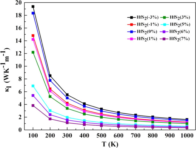
Calculated lattice thermal conductivity of monolayer HfS2 as a function of carrier concentration at different biaxial strains.
It is worth noting that we observe a large change in the lattice thermal conductivity when the strain reaches 5% and above. Therefore, we explain this phenomenon by analyzing the changes in phonon group velocity and relaxation times from Figure 8. From Figure 8a–d, the group velocity of acoustic modes is basically larger than that of the optical modes, and only the group velocity of the optical modes between 4 and 8 THz is greater than that of the acoustic modes. When the strain reaches 5% and more, the group velocity of the acoustic modes is significantly reduced, while the group velocity of the optical modes increases. Regardless of the acoustic mode or the optical mode, their frequencies decrease. Mode-dependent phonon relaxation times for ZA, LA, TA, and optical modes under different biaxial strains are shown in Figure 8e–h. The ZA, LA, TA modes have larger relaxation times than the optical modes, which indicates that the phonon scattering rate of the acoustic modes is lower than that of the optical modes. This also shows that the acoustic mode has a greater contribution to the thermal conductivity of the lattice than the optical mode. But regardless of the acoustic mode or the optical mode, their relaxation times are significantly reduced when the strain reaches 5% and more. This shows that the phonon scattering rate increases significantly when the strain reaches 5% and more. The high phonon scattering rate and low phonon group velocity also cause the lattice thermal conductivity to reduce significantly when the strain reaches 5%.
Figure 8.

Magnitude of the phonon group velocity as a function of frequency in the full BZ under different biaxial strains: (a) 0%, (b) 5%, (c) 6%, and (d) 7%. Mode-dependent phonon relaxation times for ZA, LA, TA, and optical modes under different biaxial strains: (e) 0%, (f) 5%, (g) 6%, and (h) 7%.
The calculated electronic structures of monolayer HfS2 under different strains are shown in Figure 9a–h. It is well-known that strain can modify the band structure. In this paper, we found that the tensile strain led to an increase in the band gap and a compressive strain led to a decrease in the band gap. When the biaxial stress effect is from −3 to 7%, the band gap of the system increases from 0.9 to 1.83 eV. Furthermore, the energy difference between valleys I and II (III and IV) is denoted as ΔC (ΔV), namely, ΔC = EI – EII, ΔV = EIV – EIII, where EI and EII denote the two conduction band valleys near the Fermi level, and EIII, EIV, and EV denote the three valence band valleys near the Fermi level. It is theoretically considered that ΔV less than a certain value (compared with kBT, where kB is the Boltzmann constant) represents the merging of energy levels3,5,11,13,30 and affects the thermoelectric properties of the material. The increase of the degeneracy in the valley is generally helpful to improve the thermoelectric properties of thermoelectric materials.5,26,30 This is because the multiple degenerate valleys increase the effective mass without significantly decreasing the carrier mobility.26 As can be seen from Figure 10a, ΔV decreases with increasing strain and approaches 0 eV at 5% strain. This shows that the three valleys of the valence band can be regarded as being effectively converged. In other words, the energy levels are merged.
Figure 9.

Band structure of monolayer HfS2 under different biaxial strains: (a) −3%, (b) −1%, (c) 0%, (d) 1%, (e) 3%, (f) 5%, (g) 6%, and (h) 7%. The two conduction band valleys near the Fermi level (0 eV) are denoted by I and II. The three valence band valleys near the Fermi level are denoted by III, IV, and V. ΔC (ΔV) represents the energy difference between I and II (III and IV).
Figure 10.

(a) Band gaps (Δ) and the energy difference between the conduction and valance band valleys (ΔC and ΔV, respectively) as a function of the applied biaxial strain. (b) Partial density of states of the monolayer HfS2 at 0, 5, and 7% strains.
Under the action of strain, the lattice constant of the crystal structure changed and the position of the atom also shifted, resulting in a change in the characteristics and strength of the bond between atoms so that the band structure changed. This can also be observed from the information in Figure 10b of the partial density of states (PDOS) of monolayer HfS2. The PDOSs at 0, 5, and 7% strains are calculated and compared as shown in Figure 10b. It can be seen from Figure 10b that the valance band is mainly contributed by the 3p orbital of the S atom, and in the range of energy level from 0 to −1 eV, the PDOS at 5% strain is obviously greater than the PDOS at 0 and 7% strains. Therefore, when the biaxial strain is at around 5%, the band of the monolayer HfS2 converges. Finally, the Seebeck coefficient and the power factor of p-type doping may be the highest at 5% strain. In the following, it is shown that the Seebeck coefficient and the power factor are indeed the largest under the stress of 5%, as shown in Figure 11b,c.
Figure 11.

Calculated electronic transport coefficients ((a) σ/τ, (b) S, (c) S2σ/τ, and (d) κe/τ) as a function of carrier concentration for both p-type and n-type monolayer HfS2 at different biaxial strains.
The electron transport coefficients under different strains were calculated on the basis of the semiclassical Boltzmann theory. Figure 11a shows the variation of σ/τ with carrier concentration under different strains. The σ/τ increases with increasing carrier concentration. When the biaxial strain changes from −3 to 7%, the σ/τ decreases, and the p-type conductance varies greatly with strain, while the n-type conductance varies little with strain. Moreover, we find that the σ/τ of n-type is obviously higher than that of p-type under the same conditions.
Figure 11b shows the variation of S with carrier concentration under different strains. The overall trend of S decreases with increasing carrier concentration. For p-type doping, we find that S increases with the increasing biaxial strain and becomes maximum at a strain of 5%. For n-type doping, S increases when the strain changes from −3 to 7%. Figure 11c shows the variation of S2σ/τ with carrier concentration under different strains. For p-type doping, S2σ/τ increases with the increasing strain and reaches the maximum value under 5% strain. For n-type doping, S2σ/τ increases monotonically with the increasing strain and reaches the maximum value under 7% strain. As mentioned above, the increase of the degeneracy in the valance band valley is in favor of the increase of S and S2σ/τ; that is to say, the increase of S and S2σ/τ is accompanied by the decrease of ΔC under strain from −3 to 7%, which is consistent with our results (Figure 11). Now, we have the ratio of the electronic transport coefficients and the relaxation time, and the effect of relaxation time cannot be ignored.
Figure 11d shows the variation of κe/τ with carrier concentration under different strains. For both n-type and p-type doping, we find that κe/τ decreases with the increase of strain from −3 to 7%, and the κe/τ of p-type doping is obviously smaller than that of n-type doping, especially when the strain is below 3%.
Table 3 shows the effective mass, average effective mass, elastic modulus, deformation potential constant, and relaxation time of monolayer HfS2 at −3, −1, 0, 1, 3, 5, 6, and 7% biaxial strains.
Table 3. Effective Mass (m*), Average Effective Mass (md), Elastic Modulus (C2D), Deformation Potential Constant (El), Electron and Hole Mobility (μ), and Relaxation Time (τ) of Monolayer HfS2 at −3, −1, 0, 1, 3, 5, 6, and 7% Biaxial Strains.
| carrier type | m* (m0) | md (m0) | C2D (N m–1) | El (eV) | μ (cm–2 V–1 s–1) | τ (10–14 s) | |
|---|---|---|---|---|---|---|---|
| electron | strained (−3%) | 1.29 | 4.07 | 247.49 | 1.20 | 733.5 | 53.9 |
| strained (−1%) | 1.38 | 4.41 | 218.00 | 1.15 | 607.0 | 47.7 | |
| strained (0%) | 1.43 | 4.62 | 202.72 | 1.37 | 364.2 | 29.7 | |
| strained (1%) | 1.41 | 4.83 | 187.04 | 1.14 | 450.6 | 36.2 | |
| strained (3%) | 1.58 | 5.37 | 167.31 | 1.13 | 346.1 | 31.1 | |
| strained (5%) | 1.70 | 6.12 | 146.21 | 1.07 | 275.1 | 26.6 | |
| strained (6%) | 1.76 | 6.62 | 135.36 | 1.01 | 243.0 | 24.3 | |
| strained (7%) | 1.82 | 7.20 | 130.24 | 1.47 | 103.1 | 10.7 | |
| hole | strained (−3%) | 1.45 | 0.44 | 247.49 | 15.4 | 35 | 2.89 |
| strained (−1%) | 1.45 | 0.46 | 218.00 | 13.9 | 36.2 | 2.99 | |
| strained (0%) | 1.44 | 0.44 | 202.72 | 13.3 | 38.2 | 3.10 | |
| strained (1%) | 1.45 | 0.48 | 187.04 | 12.5 | 37.5 | 3.00 | |
| strained (3%) | 1.45 | 0.50 | 167.31 | 10.9 | 43.4 | 3.58 | |
| strained (5%) | 1.97 | 0.87 | 146.21 | 4.53 | 88.7 | 9.95 | |
| strained (6%) | 1.93 | 0.86 | 135.36 | 2.09 | 398.4 | 43.8 | |
| strained (7%) | 1.90 | 0.86 | 130.24 | 2.08 | 393.1 | 42.5 |
Combining all of the calculated coefficients together, the variation of the ZT value with carrier concentration is shown in Figure 12. The ZT value of p-type doping is only 0.09 at 0% strain. Moreover, we find that the ZT value of p-type doping changes greatly with the increase of strain. When the strain increases to 7%, the ZT value reaches 3.35, with a huge improvement. The ZT value of n-type doping is 1.09 at 0% strain, which is much higher than that of p-type doping. On further applying strain to it and on reaching 6% strain, we find that the ZT value further increased to 2.29. Under biaxial strain, we find that the ZT value of p-type doping exceeds that of n-type doping when the strains are at 6 and 7%. The reason for this can be seen from Table 3; the relaxation time of p-type doping is larger than that of n-type doping, and the difference between the S2σ/τ of p-type and n-type doping is not significant. Therefore, the S2σ of p-type doping is higher than that of n-type doping. For p-type, the power factor is 35.5 mW mK–2 at 6% strain with the hole concentration at 6 × 1012 cm–2 and the power factor is 29.5 mW mK–2 at 7% strain with the hole concentration at 5 × 1012 cm–2. For n-type, the power factor is 22.9 mW mK–2 at 6% strain with the electron concentration at 4 × 1012 cm–2 and the power factor is 12.3 mW mK–2 at 7% strain with the electron concentration at 6 × 1012 cm–2. In addition, we also obtained the thermal conductivity at 6 and 7% strains. At 6% strain, the thermal conductivity of p-type and n-type doping are 3.37 and 2.99 W m–1 K–1, respectively. The thermal conductivities of p-type and n-type doping are 2.65 and 2.01 W m–1 K–1, respectively, at 7% strain. We infer from this result that the thermal conductivity differences for both n-type and p-type doped monolayer HfS2 are not particularly large. Therefore, the ZT value of p-type doping is ultimately greater than that of n-type doping at 6 and 7% strains. It can be seen that the strain in a certain range can simultaneously increase S and the power factor and can also reduce the thermal conductivity. The combined effect of these factors ultimately improves their thermoelectric performance.
Figure 12.
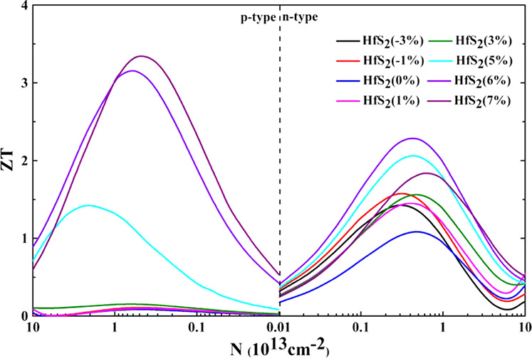
Calculated ZT as a function of carrier concentration for both p-type and n-type monolayer HfS2 at different biaxial strains.
4. Conclusions
We have studied the phonon, electronic, thermal, and thermoelectric properties of monolayer HfS2 with and without biaxial strain based on first-principles calculations combined with Boltzmann equations. At 0% strain, the results show that the ZT value of n-type HfS2 at the optimal doping concentration is 1.09, while the ZT value of p-type HfS2 is only 0.09. This indicates that the thermoelectric performance of n-type HfS2 is much higher than that of p-type HfS2 under the condition of 0% strain. Moreover, the strain can effectively improve the thermoelectric properties of materials. For n-type, the maximum ZT value is 2.29 at 6% strain, and for p-type, the maximum ZT value is 3.35 at 7% strain. This indicates that strain can greatly improve the thermoelectric performance of single-layer HfS2, especially for p-type HfS2.
At the same time, we can also see that when the strain reaches 5%, the energy level degeneracy is the strongest, resulting in the rapid increase of ZT values for p- and n-type HfS2. That is to say, the thermoelectric properties of monolayer HfS2 can be effectively enhanced by band valley engineering. It is hoped that our work can supplement and improve the two-dimensional thermoelectric material database, providing suggestions for future new material design.
Acknowledgments
The authors acknowledge the National Natural Science Foundation of China (Nos. 11504304 and 11972313) and the Project of State Key Laboratory of Environment-friendly Energy Materials, Southwest University of Science and Technology (Nos. 19fksy07 and 20fksy23) for the funding. They also thank Dr. Lei Liu (Southwest University of Science and Technology, Mianyang, Sichuan 610064, China) for guidance.
The authors declare no competing financial interest.
References
- Chen Z. G.; Han G.; Yang L.; Cheng L.; Zou J. Nanostructured thermoelectric materials:current research and future challenge. Prog. Nat. Sci.: Mater. Int. 2012, 22, 535–549. 10.1016/j.pnsc.2012.11.011. [DOI] [Google Scholar]
- Lan Y. S.; Chen X. R.; Hu C. E.; Cheng Y.; Chen Q. F. Penta-PdX2 (X = S, Se, Te) monolayers: promising anisotropic thermoelectric materials. J. Mater. Chem. A 2019, 7, 11134–11142. 10.1039/C9TA02138H. [DOI] [Google Scholar]
- Tan G.; Zhao L. D.; Kanatzidis M. G. Rationally designing high-performance bulk thermoelectric materials. Chem. Rev. 2016, 116, 12123–12149. 10.1021/acs.chemrev.6b00255. [DOI] [PubMed] [Google Scholar]
- Martín-González M.; Caballero-Calero O.; Díza-Chao P. Nanoengineering thermoelectrics for 21st century: Energy harvesting and other trends in the field. Renewable Sustainable Energy Rev. 2013, 24, 288–305. 10.1016/j.rser.2013.03.008. [DOI] [Google Scholar]
- Pei Y.; Wang H.; Snyder G. Band engineering of thermoelectric materials. Adv. Mater. 2012, 24, 6125–6135. 10.1002/adma.201202919. [DOI] [PubMed] [Google Scholar]
- Li J. F.; Liu W. S.; Zhao L. D.; Zhou M. High-performance nanostructured thermoelectric materials. NPG Asia Mater. 2010, 2, 152–158. 10.1038/asiamat.2010.138. [DOI] [Google Scholar]
- Abdollah H. M.; Mohammad Y.; Mojtaba Y.; Alireza A. Investigation into thermoelectric properties of M (M = Hf, Zr) X2 (X = S, Se, Te) nanotubes using first-principle calculations. Solid State Commun. 2021, 336, 114289 10.1016/j.ssc.2021.114289. [DOI] [Google Scholar]
- Zhao L. D.; Lo S. H.; Zhang Y.; Sun H.; Tan G.; Uher C.; Wolverton C.; Dravid V. P.; Kanatzidis M. G. Ultralow thermal conductivity and high thermoelectric figure of merit in SnSe crystals. Nature 2014, 508, 373–377. 10.1038/nature13184. [DOI] [PubMed] [Google Scholar]
- Vineis C. J.; Shakouri A.; Majumdar A.; Kanatzidis M. G. Nanostructured thermoelectircs: Big efficiency gains from small features. Adv. Mater. 2010, 22, 3970–3980. 10.1002/adma.201000839. [DOI] [PubMed] [Google Scholar]
- Yan P.; Gao G. Y.; Ding G. Q.; Qin D. Bilayer MSe2 (M = Zr, Hf) as promising two-dimensional thermoelectric materials: a first-principles study. RSC Adv. 2019, 9, 12394–12403. 10.1039/C9RA00586B. [DOI] [PMC free article] [PubMed] [Google Scholar]
- Pei Y.; Shi X.; Lalonde A.; Wang H.; Chen L.; Snyder G. J. Convergence of electronic bands for high performance bulk thermoelectrics. Nature 2011, 473, 66–69. 10.1038/nature09996. [DOI] [PubMed] [Google Scholar]
- Fang T.; Zheng S.; Zhou T.; Yan L.; Zhang P. Computational prediction of high thermoelectric performance in p-type half-heusler compounds with low band effective mass. Phys. Chem. Chem. Phys. 2017, 19, 4411–4417. 10.1039/C6CP07897D. [DOI] [PubMed] [Google Scholar]
- Zhu T.; Lin Y.; Fu C.; Heremans J. P.; Snyder J. G.; Zhao X. Compromise and synergy in high-efficiency thermoelectric materials. Adv. Mater. 2017, 29, 1605884 10.1002/adma.201605884. [DOI] [PubMed] [Google Scholar]
- Zhu T.; Fu C.; Xie H.; Liu Y.; Zhao X. High efficiency half-Heusler thermoelectric materials for energy harvesting. Adv. Energy Mater. 2015, 5, 1500588 10.1002/aenm.201500588. [DOI] [Google Scholar]
- Dresselhaus M. S.; Chen G.; Tang M. Y.; Yang R.; Lee H.; Wang D.; Ren Z.; Fleurial J.-P.; Gogna P. New directions for low-dimensional thermoelectric materials. Adv. Mater. 2007, 19, 1043–1053. 10.1002/adma.200600527. [DOI] [Google Scholar]
- Li D.; Gong Y.; Chen Y.; Lin J.; Khan Q.; Zhang Y.; Li Y.; Zhang H.; Xie H. Recent progress of two-dimensional thermoelectric materials. Nano-Micro Lett. 2020, 12, 36 10.1007/s40820-020-0374-x. [DOI] [PMC free article] [PubMed] [Google Scholar]
- Sootsman J. R.; Chung D. Y.; Kanatzidis M. G. New and old concepts in thermoelectric materials. Angew. Chem., Int. Ed. 2009, 48, 8616–8639. 10.1002/anie.200900598. [DOI] [PubMed] [Google Scholar]
- Biswas K.; He J.; Blum I. D.; Wu C. I.; Hogan T. P.; Seidman D. N.; Dravid V. P.; Kanatzidis M. G. High-performance bulk thermoelectrics with all-scale hierarchical architectures. Nature 2012, 489, 414–418. 10.1038/nature11439. [DOI] [PubMed] [Google Scholar]
- Zhao L. D.; Tan G.; Hao S.; He J.; Pei Y.; Chi H.; Wang H.; Gong S.; Xu H.; Dravid V. P.; et al. Ultrahigh power factor and thermoelectric performance in hole-doped single-crystal SnSe. Science 2016, 351, 141–144. 10.1126/science.aad3749. [DOI] [PubMed] [Google Scholar]
- Zhou Z. Z.; Liu H. J.; Fan D. D.; Cao G. H.; Sheng C. Y. High thermoelectric performance in the hexagonal bilayer structure consisting of light boron and phosphorus elements. Phys. Rev. B 2019, 99, 085410 10.1103/PhysRevB.99.085410. [DOI] [Google Scholar]
- Naguib M.; Mashtalir O.; Carle J.; Presser V.; Lu J.; Hultman L.; Gogotsi Y.; Barsoum M. W. Two-dimensional transition metal carbides. ACS Nano 2012, 6, 1322–1331. 10.1021/nn204153h. [DOI] [PubMed] [Google Scholar]
- Khazaei M.; Arai M.; Sasaki T.; Estili M.; Sakka Y. Two-dimensional molybdenum carbides: potential thermoelectric materials of the MXene family. Phys. Chem. Chem. Phys. 2014, 16, 7841–7849. 10.1039/C4CP00467A. [DOI] [PubMed] [Google Scholar]
- Sajjad M.; Singh N.; Sattar S.; Wolf S. De.; Schwingenschlögl U. Ultralow lattice thermal conductivity and thermoelectric properties of monolayer Tl2O. ACS Appl. Energy Mater. 2019, 2, 3004–3008. 10.1021/acsaem.9b00249. [DOI] [Google Scholar]
- Özbal G.; Senger R. T.; Sevik C.; Sevincli H. Ballistic thermoelectric properties of monolayer semiconducting transition metal dichalcogenides and oxides. Phys. Rev. B 2019, 100, 085415 10.1103/PhysRevB.100.085415. [DOI] [Google Scholar]
- Huang W.; Da H.; Liang G. Thermoelectric performance of MX2 (M = Mo, W; X = S, Se) monolayers. J. Appl. Phys. 2013, 113, 104304 10.1063/1.4794363. [DOI] [Google Scholar]
- Bera J.; Sahu S. Strain induced valley degeneracy: A route to the enhancement of thermoelectric properties of monolayer WS2. RSC Adv. 2019, 9, 25216–25224. 10.1039/C9RA04470A. [DOI] [PMC free article] [PubMed] [Google Scholar]
- Ding G.; Gao G. Y.; Huang Z.; Zhang W.; Yao K. Thermoelectric properties of monolayer MSe2 (M = Zr, Hf): low lattice thermal conductivity and a promising figure of merit. Nanotechnology 2016, 27, 375703 10.1088/0957-4484/27/37/375703. [DOI] [PubMed] [Google Scholar]
- Bera J.; Betal A.; Sahu S. Spin orbit coupling induced enhancement of thermoelectric performance of HfX2 (X = S, Se) and its Janus monolayer. J. Alloys Compd. 2021, 872, 159704 10.1016/j.jallcom.2021.159704. [DOI] [Google Scholar]
- Singh D.; Ahuja R. Enhanced optoelectronic and thermoelectric properties by intrinsic structural defects in monolayer HfS2. ACS Appl. Energy Mater. 2019, 2, 6891–6903. 10.1021/acsaem.9b01402. [DOI] [Google Scholar]
- Qin D.; Ge X. J.; Ding G. Q.; Gao G. Y.; Lv J. T. Strain-induced thermoelectric performance enhancement of monolayer ZrSe2. RSC Adv. 2017, 7, 47243–47250. 10.1039/C7RA08828K. [DOI] [Google Scholar]
- Kresse G.; Hafner F. Ab Initio molecular dynamics for liquid metals. Phys. Rev. B 1993, 47, 558–561. 10.1103/PhysRevB.47.558. [DOI] [PubMed] [Google Scholar]
- Kresse G.; Joubert D. From ultrasoft pseudopotentials to the projector augmented-wave method. Phys. Rev. B 1999, 59, 1758–1775. 10.1103/PhysRevB.59.1758. [DOI] [Google Scholar]
- Perdew J. P.; Burke K.; Ernzerhof M. Generalized gradient approximation made simple. Phys. Rev. Lett. 1996, 77, 3865. 10.1103/PhysRevLett.77.3865. [DOI] [PubMed] [Google Scholar]
- Li W.; Carrete J.; Katcho N. A.; Mingo N. ShengBTE: A solver of the Boltzmann transport equation for phonons. Comput. Phys. Commun. 2014, 185, 1747–1758. 10.1016/j.cpc.2014.02.015. [DOI] [Google Scholar]
- Togo A.; Oba F.; Tanaka I. First-Principles calculations of the ferroelastic transition between rutile-type and CaCl2-type SiO2 at high pressure. Phys. Rev. B 2008, 78, 134106 10.1103/PhysRevB.78.134106. [DOI] [Google Scholar]
- Chen X.; Wang D.; Liu X.; Li L.; Sanyal B. Two-dimensional square-A2B (A = Cu, Ag, Au, and B = S, Se): Auxetic semiconductors with high carrier mobilities and unusually low lattice thermal conductivities. J. Phys. Chem. Lett. 2020, 11, 2925–2933. 10.1021/acs.jpclett.0c00613. [DOI] [PubMed] [Google Scholar]
- Batsanov S. S. Van der Waals Radii of elements. Inorg. Mater. 2001, 37, 871–885. 10.1023/A:1011625728803. [DOI] [Google Scholar]
- Madsen G. K. H.; Singh D. J. BoltzTraP. A code for calculating band-structure dependent quantities. Comput. Phys. Commun. 2006, 175, 67–71. 10.1016/j.cpc.2006.03.007. [DOI] [Google Scholar]
- Takagi S. I.; Toriumi A.; Iwase M.; Tango H. On the universality of inversion layer mobility in Si MOSFET’s: Part I-effects of substrate impurity concentration. IEEE Trans. Electron Devices 1994, 41, 2357–2362. 10.1109/16.337449. [DOI] [Google Scholar]
- Zhang W. X.; Huang Z. S.; Zhang W. L.; Li Y. R. Two-dimensional semiconductors with possible high room temperature mobility. Nano Res. 2014, 7, 1731–1737. 10.1007/s12274-014-0532-x. [DOI] [Google Scholar]
- Hodul D. T.; Stacy A. M. Anomalies in the properties of Hf(S2-xTex)1-y and Hf(Se2-xTex)1-y near the metal-insulator transition. J. Solid State Chem. 1984, 54, 438–446. 10.1016/0022-4596(84)90176-2. [DOI] [Google Scholar]
- Obeid M. M.; Bafekry A.; Rehman S. Ur.; Nguyen C. V. A type-II GaSe/HfS2 van der Waals heterostructure as promising photocatalyst with high carrier mobility. Appl. Surf. Sci. 2020, 534, 147607 10.1016/j.apsusc.2020.147607. [DOI] [Google Scholar]
- Faghihnasiri M.; Ahmadi A.; Alvankar Golpayegan S.; Garosi Sharifabadi S.; Ramazani A. A first-principles study of nonlinear elastic behavior and anisotropic electronic properties of two-dimensional HfS2. Nanomaterials 2020, 10, 446 10.3390/nano10030446. [DOI] [PMC free article] [PubMed] [Google Scholar]
- Peng J.; Najmaei S.; Dubey M.; Chung P. W. Dominant ZA phonons and thermal carriers in HfS2. J. Appl. Phys. 2019, 126, 164302 10.1063/1.5110515. [DOI] [Google Scholar]
- Gu X.; Yang R. Phonon transport in single-layer transition metal dichalcogenides: A first-principles study. Appl. Phys. Lett. 2014, 105, 131903 10.1063/1.4896685. [DOI] [Google Scholar]
- Jin Z.; Liao Q.; Fang H.; Liu Z.; Liu W.; Ding Z.; Luo T.; Yang N. A Revisit to high thermoelectric performance of single-layer MoS2. Sci. Rep. 2015, 5, 18342 10.1038/srep18342. [DOI] [PMC free article] [PubMed] [Google Scholar]
- Han D.; Yang X.; Du M.; Xin G.; Zhang J.; Wang X.; Cheng L. Improved thermoelectric properties of WS2-WSe2 phononic crystals: insights from first-principles calculations. Nanoscale 2021, 13, 7176–7192. 10.1039/D0NR09169C. [DOI] [PubMed] [Google Scholar]
- Kaur H.; Yadav S.; Srivastava A. K.; Singh N.; Rath S.; Schneider J. J.; Sinha O. P.; Srivastava R. High-Yield Synthesis and Liquid-Exfoliation of Two-Dimensional Belt-Like Hafnium Disulphide. Nano Res. 2018, 11, 343–353. 10.1007/s12274-017-1636-x. [DOI] [Google Scholar]