

Abstract

Metallic two-dimensional (2D) transition metal dichalcogenides (TMDCs) are attracting great attention because of their interesting low-temperature properties such as superconductivity, magnetism, and charge density waves (CDW). However, further studies and practical applications are being slowed down by difficulties in synthesizing high-quality materials with a large grain size and well-determined thickness. In this work, we demonstrate epitaxial chemical vapor deposition (CVD) growth of 2D NbS2 crystals on a sapphire substrate, with a thickness-dependent structural phase transition. NbS2 crystals are epitaxially aligned by the underlying c-plane sapphire resulting in high-quality growth. The thickness of NbS2 is well controlled by growth parameters to be between 1.5 and 10 nm with a large grain size of up to 500 μm. As the thickness increases, we observe in our NbS2 a transition from a metallic 3R-polytype to a superconducting 2H-polytype, confirmed by Raman spectroscopy, aberration-corrected scanning transmission electron microscopy (STEM) and electrical transport measurements. A Berezinskii–Kosterlitz–Thouless (BKT) superconducting transition occurs in the CVD-grown 2H-phase NbS2 below the transition temperature (Tc) of 3 K. Our work demonstrates thickness and phase-controllable synthesis of high-quality superconducting 2D NbS2, which is imperative for its practical applications in next-generation TMDC-based electrical devices.
Keywords: two-dimensional superconductors, phase transition, CVD, transition metal dichalcogenides, niobium disulfide
Introduction
Semiconducting two-dimensional (2D) transition metal dichalcogenides (TMDCs) have been heavily studied because of their layer-number-dependent bandgap1 and outstanding performance as field-effect transistors2 and optoelectronic devices.3 In contrast to semiconducting TMDCs, metallic TMDCs (e.g., NbS2, NbSe2) are attracting great attention in the context of realizing 2D metal–semiconductor junctions with semiconducting TMDCs4,5 with the aim of lowering contact resistance by weakening Fermi level pinning.6 They are expected to be ideal 2D metal electrodes thanks to their van der Waals (vdW) interaction and small lattice mismatch with other TMDCs,7 enhancing electrical performance compared with conventional 3D metal electrodes. Additionally, these metallic TMDCs hold interesting low-temperature properties such as superconductivity,8,9 magnetism,10 and charge density waves11,12 (CDW), where superconducting TMDCs could be used to observe Andreev reflection in 2D systems13,14 and realize Josephson junctions.15 Among metallic TMDCs, 2H-NbS2 is a peculiar case in that it is the only superconductor with no CDW instabilities observed experimentally.8 This is unusual if compared with other isostructural and isoelectronic compounds such as 2H-NbSe2 and 2H-TaS2, where superconductivity coexists with CDW order. Theoretical work, however, points out that 2H-NbS2 is on the verge of CDW order in the 2D limit16 or even close to spin density wave instabilities17 possibly induced by magnetic impurities.18 This makes 2D NbS2 an appealing material platform to explore quantum phase transition. These interesting electronic properties and its potential device applications motivate the development of methods to synthesize 2D metallic and superconducting NbS2.
Niobium disulfide (NbS2) mainly exists in two polytypes: rhombohedral (3R) and hexagonal (2H), which exhibit distinct electrical properties. In 3R-NbS2, metallicity has been confirmed with a minimum resistance at around 30 K.19 On the other hand, superconductivity can be observed in bulk 2H-NbS2 below the transition temperature (Tc) of 6 K.8 These two phases can be selectively grown in bulk by changing the sulfur pressure,20 whereas reports on control over the polytypes in the few-layer limit are rare. Although 2D NbS2 can be obtained by mechanical exfoliation from bulk crystals,21,22 the flakes are usually several μm in size with little control over the thickness. In recent years, several attempts for growing NbS2 using CVD have been reported.19,23,24 Nevertheless, only 3R-phase metallic NbS2 has been grown, with a limited domain size and lack of precise layer number control. Growing large-grain and superconducting 2H-phase NbS2 with controllable thickness has not been reported yet, hindering the exploration of 2D superconducting properties and further applications in electrical devices.
Here, we demonstrate epitaxial CVD growth of 2D NbS2 single crystals and continuous transition from a metallic 3R-polytype to superconducting 2H-polytype with respect to its thickness. Our NbS2 flakes have a rectangular shape with a large grain size exceeding 500 μm and are highly aligned by quasi van der Waals epitaxy with an atomically smooth sapphire surface. The thickness can be tuned from 1.5 to 10 nm by changing the growth conditions. The thickness-dependent phase transition was clearly observed from Raman and STEM study, which is further confirmed by transport measurements for different phases, including the observation of superconductivity in layered 2H-NbS2 below a transition temperature of 3 K.
Results and Discussion
2D NbS2 Grown by CVD
2D NbS2 was grown using a home-built CVD reactor schematically presented in Figure 1a. C-plane sapphire was used as the growth substrate and was annealed in air for 6 h prior to growth, resulting in a clean surface with atomically smooth step terraces,25 which is crucial for achieving epitaxial growth.26 A solution of niobium chloride (NbCl5) was used as the precursor, while sodium chloride (NaCl) was used to reduce nucleation density27 and the reaction energy barrier.28 Both solvents were spin-coated on top of sapphire substrate before loading into the chamber. During the growth, as shown in Figure 1a, another bare sapphire wafer was placed on top of the spin-coated wafer. This promotes the growth of larger crystals by localizing the NbCl5 vapor and reducing the flow rate of H2S near the substrate.
Figure 1.

CVD growth of layered NbS2 flakes. (a) Schematic illustration of the hot-wall CVD system for NbS2 growth. In the chamber, a bare wafer was placed on top of the sapphire wafer, which was spin-coated with NaCl and NbCl5 solutions. (b) Optical micrographs of as-grown NbS2 flakes showing rectangular shapes and a large size exceeding 500 μm. The orientation of rectangular NbS2 flakes is aligned in the same direction. (c) AFM image of the as-grown NbS2 on a sapphire substrate, from an area shown in (b). NbS2 seeds are epitaxially aligned along the [11̅00] axis of c-plane sapphire, while the preferred growth orientation of rectangular NbS2 flakes is determined by the terrace step edges.
We observe different morphologies of our CVD-grown NbS2 crystals, depending on the growth parameters. Optical micrographs of CVD-grown NbS2 crystals are shown in Figure 1b and Supplementary Figure S1. As can be seen from the figures, the shape and thickness of NbS2 flakes show a clear trend, changing from thick triangles to thin rectangles with increasing temperature. It is notable that the rectangle-shaped NbS2 flakes are grown with a large domain size having a typical length exceeding 500 μm and a width of around 40 μm, which is significantly larger than those in previous reports.19,23,29 In addition, all the rectangular NbS2 flakes are perfectly aligned in the same direction, confirmed by the orientation histogram shown in Supplementary Figure S2 for the same region as shown in Figure 1b. The single-crystalline structure was confirmed by selected area electron diffraction (SAED) patterns on several areas of an NbS2 flake as shown in Supplementary Figure S3. The different crystal morphologies and the orientation of rectangular NbS2 can be explained by the temperature-dependent strong interaction between NbS2 and the sapphire substrate.30 At the early stage of growth, nucleation takes place on the surface of sapphire with an initial random orientation of the crystallites.31 For relatively low growth temperatures (e.g., 750 °C), the small crystallites do not have enough thermal energy to explore the energy landscape by rotation before they grow to big crystals. As a result, NbS2 crystals with a small domain size and a random orientation are observed in Supplementary Figure S1a. We also observe a higher nucleation density under these conditions because of weak thermal etching. However, at higher growth temperatures (850 and 950 °C, Supplementary Figure S1b and Figure 1b), the orientation of the grown NbS2 is determined by the underlying sapphire. This could be related to the orientation of step edges on the atomically smooth sapphire surface. An AFM image of rectangular NbS2 crystals from the sample shown in Figure 1b is presented in Figure 1c, which clearly shows that the long edges of the NbS2 crystal are oriented along the step edges on the surface of sapphire. In addition, we note that the smaller triangular NbS2 crystals both on sapphire and on the NbS2 thin film are epitaxially aligned along the [11̅00] axis of the underlying c-plane sapphire (see Supplementary Figure S5), which can be explained by van der Waals interaction with the underlying substrate.32
Growth morphologies can also be modulated by the gas flow ratio of H2S and Ar. Dendritic NbS2 crystals were observed in Supplementary Figure S1c,d with a relatively lower value of H2S:Ar compared with that in Figure 1b. The morphology transition induced by the gas flow ratio can be explained by the growth rates of different edge terminations.33 In our case, the NbCl5 precursor is reduced by H2S and tiny NbS2 seeds emerge at the early stage of growth. Along the edges of these tiny seeds, Nb and S atoms are exposed to the reactor atmosphere on zigzag edges33 with high chemical reactivity. They encounter atoms diffusing on the surface in random collisions and new chemical bonds are formed to achieve the most energetically stable structure.34 Assuming that the spin-coated NbCl5 provides the same amount of Nb precursor, the probability of meeting and bonding with free atoms depends on the partial pressure of H2S. When the sulfur supply rate is at an insufficient level (e.g., H2S: Ar = 1:8), S-terminated edges have much higher possibility to meet free Nb atoms, which leads to a higher growth rate of S-terminated edges than Nb-terminated edges. The difference in growth rates causes the dendritic shapes shown in Supplementary Figure S1c,d. As H2S increases to a saturated level (e.g., H2S: Ar = 1:3), both S- and Nb-terminated edges have enough opportunity to bond with free atoms, resulting in similar growth rates of these two types of edges. As a consequence, crystals grow with regular shapes and sharp edges as shown in Figure 1b.
Different Phases of CVD-Grown NbS2
We find that our CVD-grown rectangular NbS2 crystals can have both 3R and 2H-phase structures, depending on the thickness. Figure 2a illustrates the atomic structures of NbS2 with 3R and 2H polytype stacking. Each layer is composed of a 1H single layer where the Nb atoms are coordinated in a trigonal prismatic shape, while adjacent layers interact via the van der Waals force and maintain the interlayer distance of around 0.7 nm.29 The two polytypes are distinguished by relative rotation and atom alignment between the neighboring planes.35 Atomic force microscopy (AFM), Raman spectroscopy and aberration-corrected STEM were further conducted to investigate the correlation between the phase transition and thickness.
Figure 2.

Phase transition of CVD-grown NbS2 flakes. (a) Side and top views of atomic structures of NbS2 with 3R-polytype stacking and 2H-polytype stacking. (b) AFM image of an NbS2 flake transferred onto a Si/SiO2 substrate. Inset shows the thickness of NbS2 to be 10 nm. (c) Raman spectra at room temperature for as-grown NbS2 flakes on sapphire substrate. The blue curve corresponds to the 3R-phase in 3 nm-thick NbS2 flakes, and the orange curve shows the 2H-phase in 10 nm-thick NbS2. The purple curve corresponds to a mixture of 2H and 3R phase in 4 nm-thick NbS2. (d–f) STEM images of NbS2 flakes with (d) 3R-polytype stacking, (e) 2H-polytype stacking and (f) a mixture of 3R-polytype stacking and 2H-polytype stacking. Inset of (d): A low magnification ADF-STEM image of a NbS2 flake transferred onto a TEM grid.
Changing the NbCl5 concentration allows us to control the thickness of rectangular NbS2 crystals in the 1.5 to 10 nm range, corresponding to 2–14 layers. A histogram of the thickness distribution of as-grown NbS2 crystals for different pre-coated NbCl5 concentrations is shown in Supplementary Figure S6, indicating that a higher NbCl5 concentration leads to a higher dominant thickness. In Figure 2b, we show an AFM image of a rectangular NbS2 single crystal with a thickness of 10 nm. A smooth surface and sharp edge can be clearly seen, indicating that our NbS2 samples have a high crystallinity and good quality. Additional AFM images with various thicknesses ranging from 1.5 to 10 nm are shown in Supplementary Figure S7. Figure 2c shows the room-temperature Raman spectra acquired from as-grown rectangular NbS2 crystals with various thicknesses on sapphire substrates. The blue curve presents the Raman spectrum from 3 nm-thick NbS2 showing two characteristic peaks at 348 cm–1 (E2) and 389 cm–1 (A1), which corresponds to the 3R-phase NbS2.36 The orange curve, however, collected from 10 nm-thick NbS2 is characterized by peaks located at 340 cm–1 (E12g) and 379 cm–1 (A1g), in agreement with the spectral signature of the 2H-phase NbS2.36 Data from the 4 nm-thick NbS2 (purple curve) shows a mixture of Raman spectra for both 3R-phase and 2H-phase, indicating the transition between 2H and 3R occurs around this thickness.
The atomic structures of different phases and stackings can be directly visualized by employing aberration-corrected STEM. In Figure 2d–f, we show high-resolution high-angle annular dark-field (HAADF) STEM images obtained from transferred NbS2 samples to distinguish different atomic structures and stacking arrangements with various thicknesses. The inset of Figure 2d shows a low-magnification HAADF image of a rectangular NbS2 crystal transferred onto a TEM grid. The HAADF intensity is proportional to the square of the atomic number (∼Z2), allowing Nb and S atoms to be directly distinguished on the basis of the contrast of individual atomic columns. In Figure 2d, bright hexagonal rings (Nb atoms) with darker spots (S atoms) in the center are displayed, indicating that the Nb atoms mismatch slightly without any rotation between adjacent layers (illustrated in Figure 2a), corresponding to a 3R-polytype stacking. On the other hand, an equal intensity of each Nb atom in Figure 2e reveals that they are aligned to each other with an opposite direction between adjacent layers (illustrated in Figure 2a) and that 3 Nb atoms can be found around a single S atom, suggesting a 2H-polytype stacking. Additionally, a mixture of 3R and 2H polytype stacking is observed in Figure 2f. S line defects are visible close to the interfaces of different stackings, whereas S point defects are present everywhere in the image. A few of the defect positions are highlighted by yellow circles in the corresponding filtered image in Supplementary Figure S9. Additionally, energy-dispersive X-ray spectrometry (EDX) and elemental mapping were also carried out on the transferred samples to confirm the chemical composition and material quality (see Supplementary Figure 10).
Electrical Transport in 2D NbS2 with Different Phase Structures
In order to characterize the electrical transport properties of CVD-grown NbS2 crystals with different phases, multiterminal devices were fabricated after the crystals have been transferred onto a Si/SiO2 substrate. Figure 3a displays an optical micrograph of a Hall bar device based on a 10 nm-thick NbS2 crystal. NbS2 devices with various other thicknesses are shown in Supplementary Figure S11. The detailed fabrication process can be found in the Methods section.
Figure 3.

Transport properties of CVD-grown 2D NbS2. (a) Optical micrograph of a NbS2 device fabricated on Si/SiO2 substrate with a flake thickness of 10 nm. Scale bar length: 25 μm. (b) Zero-field cooled resistance as a function of temperature for NbS2 devices with different thicknesses. An AC current of 0.1 μA is used to probe the resistance. Inset: a zoomed-in temperature dependence of resistance from 1.4 K to 10 K. (c) V–I characterization of NbS2 devices with different thicknesses at the base temperature of 1.4 K.
To examine the relationship between the thickness-dependent structural phase and its transport properties, temperature dependence of four-probe longitudinal resistance (Rxx) was measured at zero magnetic field and the results for three representative thicknesses (3, 4, and 10 nm) shown in Figure 3b. The inset shows the magnified view in the 1.5–10 K temperature range. For the sample with a thickness of 3 nm (blue curve), the resistance linearly decreases as the temperature is lowered, indicating its metallic property (dR/dT > 0), which is consistent with previous predictions.37 However, its resistance starts to slightly increase below 20 K, where the resistance minimum is observed (see Supplementary Figure S12). Similar observations of this low-temperature resistance minimum were reported in CVD-grown 3R-phase NbS2,19,29 which is attributed to electron scattering at defect or excess Nb sites. From the device, we do not observe the superconducting transition above our experimental base temperature (1.4 K). These electrical properties agree well with the metallic nature of the 3R-phase NbS2. On the other hand, for the 2H-phase sample with a thickness of 10 nm (shown as orange curve), the resistance drops sharply to zero at around 3 K, indicating the superconducting transition. The superconducting transition critical temperature Tc is 2.6 K, which corresponds to the temperature at which the resistance becomes half of the normal-state resistance (RN), R(Tc) = 0.5 RN. At the intermediate thickness (4 nm) between the 2H and 3R phase of NbS2 (shown as the purple curve), interestingly, the resistance drops sharply at around 3 K but remains at a relatively high value (∼150 Ω) down to the base temperature of 1.4 K. This feature could be explained by the presence of mixed 2H and 3R phases where metallic 3R-phase and superconducting 2H-phase domains coexist. Magnetic field cooling suppresses this sharp resistance drop (shown in Supplementary Figure S13), which further supports the hypothesis that the resistance drop is related to the superconducting transition of the 2H domains. Notably, this 4 nm-thick device shows metallic behavior at high temperatures but with a slower resistance change (dR/dT) than that of the other 2H and 3R devices. This leads to a low residual resistance ratio (RRR) of ∼1.5, defined as the ratio between the resistance at T = 300 K and the normal-state resistance above the superconducting transition temperature of the 2H phase, at T = 10 K, which is lower than that of the 3 nm-thick 3R-phase (∼3.3) and 10 nm-thick 2H phase (∼11). Since RRR is commonly used as an indicator of the crystalline quality of a superconductor,38,39 a smaller RRR in 4 nm-thick NbS2 indicates the existence of additional structural disorder, which we attribute to sulfur point and line defects between 2H and 3R phases, as confirmed by the STEM results shown in Supplementary Figure S9. Figure 3c displays four-probe DC V–I characteristics for NbS2 with different structural phase at the base temperature (1.4 K). A linear curve was obtained for the 3 nm-thick 3R-phase NbS2 sample, whereas a strong nonlinear curve was obtained for the 10 nm-thick 2H-phase NbS2, consistent with a Berezinskii–Kosterlitz–Thouless (BKT) type superconducting phase transition. Compared with single-phase samples, the V–I curve of the 4 nm-thick sample shows a weak nonlinear curve (a possible combination of 2H and 3R-phase signals) but with a larger noise, which could be related to contributions from line defects separating the two phases. These results, consistent with Raman and STEM results, provide additional evidence that transition from the metallic 3R-polytype to the superconducting 2H-polytype takes place in our thickness-controlled CVD-grown NbS2 crystals.
Superconductivity of 2H-Phase NbS2
To further
study the superconductivity of CVD-grown 2H-phase NbS2 crystals,
both four-probe DC and AC transport measurements were performed. Figure 4a shows the temperature
dependence of resistance (Rxx) of the device shown in Figure 3a at various out-of-plane external magnetic fields B, applied perpendicularly to the 2D crystal plane. In the
presence of the magnetic field, we define the critical temperature Tc as the temperature at which the resistance
decreases to 80% of the normal-state resistance value. As the amplitude
of the magnetic field increases, the critical transition temperature
decreases and the resistance change becomes more gradual. A metallic
behavior without resistance drop was obtained above the magnetic field
of 0.6 T, indicating that superconductivity is completely suppressed
by the magnetic field. Figure 4b shows the magnetic field-dependent transition, Bc2 vs Tc/Tc0 phase diagram where Hc2 is the upper critical field and Tc0 the
critical temperature at zero magnetic field. We find a linear relation
between Hc2 and Tc, which is a typical feature
of 2D superconductors.40,41 It can be fitted with a model
from the linearized Ginzburg–Landau (GL) theory,42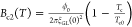 , where ξGL (0) is zero-temperature
coherence length, and ϕ0 is magnetic flux quantum.
From the fitted result, we get ξGL (0)= 25 nm, which
is larger than the probed sample thickness (10 nm). This indicates
that the 2D superconducting transition should follow the BKT type
transition. Figure 4c shows the four-probe DC I–V characteristics as a function of temperature for the 6 nm-thick
2H-phase NbS2 device. At 3.5 K, linear Ohmic behavior was
obtained with the constant slope of resistance around 3 Ω, which
is equal to the metallic normal-state resistance (shown in Supplementary Figure S14). As the temperature
decreases, the curve becomes nonlinear and a critical current gap
is observed at which the probe voltage is close to zero. The V–I curves plotted on a logarithmic
scale (shown in Figure 4d) display a clear transition from a V–I linear dependence to a power-law dependence (V
∝ Iα) indicating the BKT transition.
We estimate the BKT transition temperature (TBKT) to be 3 K at the value of α = 3 for our 6 nm-thick
NbS2 crystal. Fitted α values as a function of temperature
can be found in Figure 4e. The data presented above provides further evidence that our CVD-grown
2H-phase NbS2 exhibits the features expected from a 2D
superconductor.
, where ξGL (0) is zero-temperature
coherence length, and ϕ0 is magnetic flux quantum.
From the fitted result, we get ξGL (0)= 25 nm, which
is larger than the probed sample thickness (10 nm). This indicates
that the 2D superconducting transition should follow the BKT type
transition. Figure 4c shows the four-probe DC I–V characteristics as a function of temperature for the 6 nm-thick
2H-phase NbS2 device. At 3.5 K, linear Ohmic behavior was
obtained with the constant slope of resistance around 3 Ω, which
is equal to the metallic normal-state resistance (shown in Supplementary Figure S14). As the temperature
decreases, the curve becomes nonlinear and a critical current gap
is observed at which the probe voltage is close to zero. The V–I curves plotted on a logarithmic
scale (shown in Figure 4d) display a clear transition from a V–I linear dependence to a power-law dependence (V
∝ Iα) indicating the BKT transition.
We estimate the BKT transition temperature (TBKT) to be 3 K at the value of α = 3 for our 6 nm-thick
NbS2 crystal. Fitted α values as a function of temperature
can be found in Figure 4e. The data presented above provides further evidence that our CVD-grown
2H-phase NbS2 exhibits the features expected from a 2D
superconductor.
Figure 4.

Superconductivity in 2H-phase NbS2. (a) Electrical resistance of the device shown in Figure 3a at various out-of-plane magnetic fields B. (b) Corresponding Bc2 vs Tc/Tc0 diagram from the data shown in (a) with its fitting result. (c) V–I characterization for 6 nm-thick NbS2 device from the base temperature (1.4 K) to 3.6 K. (d) V–I curve in (c) replotted on a logarithmic scale showing V ∝ Iα behavior, consistent with an expected BKT model. (e) Fitting parameter α as a function of temperature from the data shown in (d). Gray dashed line corresponds to α = 3, where the BKT transition temperature (TBKT) is estimated to be 3 K for our 6 nm-thick NbS2 flake. (f) Differential resistance at zero magnetic field as a function of source-drain bias current at different temperatures for the 6 nm-thick NbS2 device.
To further investigate the superconducting critical current, AC differential resistance as a function of DC drain-source current was measured at fixed temperatures ranging from 1.5 to 3 K as shown in Figure 4f. Resistance peaks sharply at the critical current (190 μA at 1.5 K), which indicates the transition from the normal resistive state to the superconducting zero-resistance state. The critical current gradually decreases with an increasing temperature and disappears above 3 K as the sample becomes metallic.
Conclusions
We demonstrate a CVD method to synthesize 2D NbS2 single crystals with a large size, controllable thickness, and epitaxial orientation. The thickness-dependent structural transition from metallic 3R-phase to superconducting 2H-phase was first observed in CVD-grown NbS2 and was confirmed by Raman spectroscopy, aberration-corrected STEM as well as transport measurements. The CVD-grown 2H-phase NbS2 behaves as a 2D superconductor, with BKT-type superconducting transition occurring below 3 K. Our work demonstrates a practical approach to phase-controllable growth of 2D TMDC superconductors for their widespread use in mesoscopic devices.
Methods
Material Synthesis
Rectangular NbS2 single crystals were synthesized using chemical vapor deposition (CVD) method in the home-built system schematically represented in Figure 1a. Before growth, c-plane sapphire wafers were annealed in air for 6 h and spin-coated with 0.3 mol/L NaCl solution in deionized water as well as NbCl5 solution in isopropanol (IPA). Afterward, a sapphire wafer was loaded into the quartz chamber and covered with another bare sapphire wafer. Prior to growth, the reactor tube was purged with argon to remove residual oxygen and humidity. During the whole growth process, hydrogen disulfide (H2S) with a flow rate of 35 sccm was delivered to the chamber by using argon as a carrier gas. The growth procedure lasts for 30 min at the temperature of 950 °C and atmospheric pressure. As soon as the growth is finished, the chamber is allowed to cool down naturally. H2S flow was kept with a flow rate of 5 sccm until the furnace reached the temperature of 150 °C to reduce sulfur vacancies.
Raman Spectroscopy
Raman spectra of the NbS2 flakes were performed on as-grown samples on sapphire substrates. A spectrometer (Renishaw inVia Confocal Raman Microscope) was utilized to collect the spectrum with a 532 nm laser and a grating of 3000 g/mm at room temperature. The excitation spot size is around 1 μm with a power of 1 mW.
Scanning Transmission Electron Microscopy Measurements
The as-grown samples were spin-coated with PMMA (poly(methyl methacrylate)) A4 at a speed of 2000 rpm for 60 s and heated on a hot plate for drying at 180 °C for 5 min. After immerging in water for 5 min, the PMMA film together with NbS2 samples was detached by water tension and picked up using a silicon nitride TEM grid. Subsequently, the samples were baked on a hot plate for drying and promoting the adhesion at 65 °C for 10 min. Finally, the PMMA film was removed by immersing in acetone overnight followed by annealing in high vacuum at 250 °C for 6 h.
High-resolution high-angle annular dark filed (HAADF) STEM imaging was performed using a double aberration-corrected FEI Titan Themis, which is equipped with a X-FEG, Super-X EDX detector, and monochromator. The beam convergence half angle was set to 20 mrad which corresponds to the HAADF detector 49.5–198 mrad collection angle. The microscope was operated at an accelerating voltage of 80 kV, which is below the electron-beam induced knock-on damage of NbS2. The electron probe current was set to ∼20 pA. To avoid the sample drift, images were acquired at various places using a raster scan with 512 × 512 pixels and 8 μs dwell times. EDX measurements were performed in both Titan Themis and FEI Talos TEM. EDX spectrum and elemental mapping were processed in Velox software, ThermoFisher Scientific. Inverse fast Fourier transform filtering has been applied to magnified images to enhance the contrast and highlight the atomic structures of different phases.
Sample Transfer and Device Fabrication
The as-grown NbS2 flakes were transferred from sapphire to SiO2/Si substrate by using the same method as for the preparation of TEM samples. Afterward, the samples were spin-coated with PMMA polymer and put on a hot plate at 180 °C for 5 min. Electron-beam lithography was used to pattern the electrodes. Finally, a stack of 2 nm/80 nm thick Ti/Au was deposited by e-beam evaporation for the electrodes, followed with a lift-off process with acetone to remove the PMMA layer. Between the fabrication steps, samples were kept in the inert Ar environment inside a glovebox to prevent sample degradation in air.
Transport Measurements
Cryogenic electrical transport measurements were performed in ICE Oxford liquid helium continuous flow system with the base temperature of ∼1.4 K. Temperature dependent four-probe longitudinal resistance (Rxx) were measured using SR860 lock-in amplifier with an AC probe current Iac = 100 nA at 13.3 Hz. DC voltage–current (V–I) characteristics was measured by applying constant DC current with Keithley 2636b sourcemeter while measuring DC voltage with Keithley 2182a nanovoltmeter. Four-probe differential resistance (dVac/dIac) was measured using the lock-in amplifier with AC probe current Iac = 100 nA at 13.3 Hz while sweeping the DC current.
Acknowledgments
We acknowledge the help of Z. Benes (CMI) with electron-beam lithography. Device fabrication was carried out at the EPFL Center for micro and nanotechnology. Electron microscopy imaging was performed at the EPFL Interdisciplinary Centre for Electron Microscopy. This work was financially supported by the European Union’s Horizon 2020 research and innovation program under grant agreements No 829035 (QUEFORMAL) and No 785219 and 881603 (Graphene Flagship Core 2 and Core 3), European Research Council (grant no. 682332 and 899775), the Swiss National Science Foundation (grant no. 175822 and 157739) and the CCMX Materials Challenge grant “Large area growth of 2D materials for device integration”. The atomic structures shown on Figure 2a were drawn using VESTA.43
Supporting Information Available
The Supporting Information is available free of charge at https://pubs.acs.org/doi/10.1021/acsnano.1c07956.
Optical micrographs under different growth condition; histogram of orientation distribution; selected area electron diffraction; large-scale TEM images; AFM images from different areas; histogram of thickness distribution with various NbCl5 concentrations; AFM images with various thicknesses; TEM images of hexagonal NbS2 flake; EDX analysis; STEM images showing a mixture of 3R and 2H phase; optical micrographs of NbS2 devices; temperature dependent resistance of NbS2 devices (PDF)
The data that support the findings of this study are available in Zenodo at http://dx.doi.org/10.5281/zenodo.5645160.
Author Contributions
⊥ (Z.W., C.-Y.C.) These authors contributed equally
Author Contributions
A.K. initiated and supervised the work. Z.W. performed the CVD growth of NbS2 flakes with initial assistance of Y.Z. Z.W. and M.M. improved the CVD system with supervision of A.R. Z.W. fabricated the devices with initial assistance of G.M.M. C.-Y.C. and Z.W. designed and performed electrical measurements. M.T. performed STEM measurements and EDX spectroscopy. Z.W. performed AFM and Raman spectroscopy with help of H.G.J. A.K., Z.W., and C.-Y.C. analyzed the data with input from M.T. and H.J. All the authors contributed to the writing of the manuscript.
The authors declare no competing financial interest.
Supplementary Material
References
- Splendiani A.; Sun L.; Zhang Y.; Li T.; Kim J.; Chim C.-Y.; Galli G.; Wang F. Emerging Photoluminescence in Monolayer MoS2. Nano Lett. 2010, 10 (4), 1271–1275. 10.1021/nl903868w. [DOI] [PubMed] [Google Scholar]
- Radisavljevic B.; Radenovic A.; Brivio J.; Giacometti V.; Kis A. Single-Layer MoS2 Transistors. Nat. Nanotechnol. 2011, 6 (3), 147–150. 10.1038/nnano.2010.279. [DOI] [PubMed] [Google Scholar]
- Unuchek D.; Ciarrocchi A.; Avsar A.; Watanabe K.; Taniguchi T.; Kis A. Room-Temperature Electrical Control of Exciton Flux in a van der Waals Heterostructure. Nature 2018, 560 (7718), 340–344. 10.1038/s41586-018-0357-y. [DOI] [PubMed] [Google Scholar]
- Allain A.; Kang J.; Banerjee K.; Kis A. Electrical Contacts to Two-Dimensional Semiconductors. Nat. Mater. 2015, 14 (12), 1195–1205. 10.1038/nmat4452. [DOI] [PubMed] [Google Scholar]
- Ding X.; Zhang S.; Zhao M.; Xiang Y.; Zhang K. H. L.; Zu X.; Li S.; Qiao L. NbS2: A Promising p-Type Ohmic Contact for Two-Dimensional Materials. Phys. Rev. Appl. 2019, 12 (6), 064061. 10.1103/PhysRevApplied.12.064061. [DOI] [Google Scholar]
- Liu Y.; Stradins P.; Wei S.-H. Van Der Waals Metal-Semiconductor Junction: Weak Fermi Level Pinning Enables Effective Tuning of Schottky Barrier. Science Advances 2016, 2 (4), e1600069. 10.1126/sciadv.1600069. [DOI] [PMC free article] [PubMed] [Google Scholar]
- Geim A. K.; Grigorieva I. V. Van der Waals Heterostructures. Nature 2013, 499 (7459), 419–425. 10.1038/nature12385. [DOI] [PubMed] [Google Scholar]
- Guillamón I.; Suderow H.; Vieira S.; Cario L.; Diener P.; Rodière P. Superconducting Density of States and Vortex Cores of 2H-NbS2. Phys. Rev. Lett. 2008, 101 (16), 166407. 10.1103/PhysRevLett.101.166407. [DOI] [PubMed] [Google Scholar]
- Yokoya T.; Kiss T.; Chainani A.; Shin S.; Nohara M.; Takagi H. Fermi Surface Sheet-Dependent Superconductivity in 2H-NbSe2. Science 2001, 294 (5551), 2518–2520. 10.1126/science.1065068. [DOI] [PubMed] [Google Scholar]
- Zhu X.; Guo Y.; Cheng H.; Dai J.; An X.; Zhao J.; Tian K.; Wei S.; Cheng Zeng X.; Wu C.; Xie Y. Signature of Coexistence of Superconductivity and Ferromagnetism in Two-Dimensional NbSe2 Triggered by Surface Molecular Adsorption. Nat. Commun. 2016, 7 (1), 11210. 10.1038/ncomms11210. [DOI] [PMC free article] [PubMed] [Google Scholar]
- Chatterjee U.; Zhao J.; Iavarone M.; Di Capua R.; Castellan J. P.; Karapetrov G.; Malliakas C. D.; Kanatzidis M. G.; Claus H.; Ruff J. P. C.; Weber F.; van Wezel J.; Campuzano J. C.; Osborn R.; Randeria M.; Trivedi N.; Norman M. R.; Rosenkranz S. Emergence of Coherence in the Charge-Density Wave State of 2H -NbSe2. Nat. Commun. 2015, 6 (1), 6313. 10.1038/ncomms7313. [DOI] [PMC free article] [PubMed] [Google Scholar]
- Leroux M.; Cario L.; Bosak A.; Rodière P. Traces of Charge Density Waves in NbS2. Phys. Rev. B: Condens. Matter Mater. Phys. 2018, 97 (19), 195140. 10.1103/PhysRevB.97.195140. [DOI] [Google Scholar]
- Majumdar A.; VanGennep D.; Brisbois J.; Chareev D.; Sadakov A. V.; Usoltsev A. S.; Mito M.; Silhanek A. V.; Sarkar T.; Hassan A.; Karis O.; Ahuja R.; Abdel-Hafiez M. Interplay of Charge Density Wave and Multiband Superconductivity in Layered Quasi-Two-Dimensional Materials: The Case of NbS2 and NbSe2. Phys. Rev. Materials 2020, 4 (8), 084005. 10.1103/PhysRevMaterials.4.084005. [DOI] [Google Scholar]
- Lv P.; Zhou Y.-F.; Yang N.-X.; Sun Q.-F. Magnetoanisotropic Spin-Triplet Andreev Reflection in Ferromagnet-Ising Superconductor Junctions. Phys. Rev. B: Condens. Matter Mater. Phys. 2018, 97 (14), 144501. 10.1103/PhysRevB.97.144501. [DOI] [Google Scholar]
- Dvir T.; Zalic A.; Fyhn E. H.; Amundsen M.; Taniguchi T.; Watanabe K.; Linder J.; Steinberg H. Planar Graphene-NbSe2 Josephson Junctions in a Parallel Magnetic Field. Phys. Rev. B: Condens. Matter Mater. Phys. 2021, 103 (11), 115401. 10.1103/PhysRevB.103.115401. [DOI] [Google Scholar]
- Bianco R.; Errea I.; Monacelli L.; Calandra M.; Mauri F. Quantum Enhancement of Charge Density Wave in NbS2 in the Two-Dimensional Limit. Nano Lett. 2019, 19 (5), 3098–3103. 10.1021/acs.nanolett.9b00504. [DOI] [PubMed] [Google Scholar]
- Güller F.; Vildosola V. L.; Llois A. M. Spin Density Wave Instabilities in the NbS2 Monolayer. Phys. Rev. B: Condens. Matter Mater. Phys. 2016, 93 (9), 094434. 10.1103/PhysRevB.93.094434. [DOI] [Google Scholar]
- van Loon E. G. C. P.; Rösner M.; Schönhoff G.; Katsnelson M. I.; Wehling T. O. Competing Coulomb and Electron–Phonon Interactions in NbS2. npj Quant Mater. 2018, 3 (1), 1–8. 10.1038/s41535-018-0105-4. [DOI] [Google Scholar]
- Zhao S.; Hotta T.; Koretsune T.; Watanabe K.; Taniguchi T.; Sugawara K.; Takahashi T.; Shinohara H.; Kitaura R. Two-Dimensional Metallic NbS2: Growth, Optical Identification and Transport Properties. 2D Mater. 2016, 3 (2), 025027. 10.1088/2053-1583/3/2/025027. [DOI] [Google Scholar]
- Fisher W. G.; Sienko M. J. Stoichiometry, Structure, and Physical Properties of Niobium Disulfide. Inorg. Chem. 1980, 19 (1), 39–43. 10.1021/ic50203a009. [DOI] [Google Scholar]
- Izawa K.; Ida S.; Unal U.; Yamaguchi T.; Kang J.-H.; Choy J.-H.; Matsumoto Y. A New Approach for the Synthesis of Layered Niobium Sulfide and Restacking Route of NbS2 Nanosheet. J. Solid State Chem. 2008, 181 (2), 319–324. 10.1016/j.jssc.2007.12.002. [DOI] [Google Scholar]
- Benameur M. M.; Radisavljevic B.; Heron J. S.; Sahoo S.; Berger H.; Kis A. Visibility of Dichalcogenide Nanolayers. Nanotechnology 2011, 22 (12), 125706. 10.1088/0957-4484/22/12/125706. [DOI] [PubMed] [Google Scholar]
- Zhang Y.; Yin L.; Chu J.; Shifa T. A.; Xia J.; Wang F.; Wen Y.; Zhan X.; Wang Z.; He J. Edge-Epitaxial Growth of 2D NbS2-WS2 Lateral Metal-Semiconductor Heterostructures. Adv. Mater. 2018, 30 (40), 1803665. 10.1002/adma.201803665. [DOI] [PubMed] [Google Scholar]
- Kozhakhmetov A.; Choudhury T. H.; Al Balushi Z. Y.; Chubarov M.; Redwing J. M. Effect of Substrate on the Growth and Properties of Thin 3R NbS2 Films Grown by Chemical Vapor Deposition. J. Cryst. Growth 2018, 486, 137–141. 10.1016/j.jcrysgro.2018.01.031. [DOI] [Google Scholar]
- Yoshimoto M.; Maeda T.; Ohnishi T.; Koinuma H.; Ishiyama O.; Shinohara M.; Kubo M.; Miura R.; Miyamoto A. Atomic-Scale Formation of Ultrasmooth Surfaces on Sapphire Substrates for High-quality Thin-film Fabrication. Appl. Phys. Lett. 1995, 67 (18), 2615–2617. 10.1063/1.114313. [DOI] [Google Scholar]
- Dumcenco D.; Ovchinnikov D.; Marinov K.; Lazić P.; Gibertini M.; Marzari N.; Sanchez O. L.; Kung Y.-C.; Krasnozhon D.; Chen M.-W.; Bertolazzi S.; Gillet P.; Fontcuberta i Morral A.; Radenovic A.; Kis A. Large-Area Epitaxial Monolayer MoS2. ACS Nano 2015, 9 (4), 4611–4620. 10.1021/acsnano.5b01281. [DOI] [PMC free article] [PubMed] [Google Scholar]
- Kim H.; Ovchinnikov D.; Deiana D.; Unuchek D.; Kis A. Suppressing Nucleation in Metal–Organic Chemical Vapor Deposition of MoS2 Monolayers by Alkali Metal Halides. Nano Lett. 2017, 17 (8), 5056–5063. 10.1021/acs.nanolett.7b02311. [DOI] [PubMed] [Google Scholar]
- Yang P.; Zou X.; Zhang Z.; Hong M.; Shi J.; Chen S.; Shu J.; Zhao L.; Jiang S.; Zhou X.; Huan Y.; Xie C.; Gao P.; Chen Q.; Zhang Q.; Liu Z.; Zhang Y. Batch Production of 6-Inch Uniform Monolayer Molybdenum Disulfide Catalyzed by Sodium in Glass. Nat. Commun. 2018, 9 (1), 979. 10.1038/s41467-018-03388-5. [DOI] [PMC free article] [PubMed] [Google Scholar]
- Wang X.; Lin J.; Zhu Y.; Luo C.; Suenaga K.; Cai C.; Xie L. Chemical Vapor Deposition of Trigonal Prismatic NbS2 Monolayers and 3R-Polytype Few-Layers. Nanoscale 2017, 9 (43), 16607–16611. 10.1039/C7NR05572B. [DOI] [PubMed] [Google Scholar]
- Song G.; Remhof A.; Theis-Bröhl K.; Zabel H. Extraordinary Adhesion of Niobium on Sapphire Substrates. Phys. Rev. Lett. 1997, 79 (25), 5062–5065. 10.1103/PhysRevLett.79.5062. [DOI] [Google Scholar]
- Ma Z.; Wang S.; Deng Q.; Hou Z.; Zhou X.; Li X.; Cui F.; Si H.; Zhai T.; Xu H. Epitaxial Growth of Rectangle Shape MoS2 with Highly Aligned Orientation on Twofold Symmetry a-Plane Sapphire. Small 2020, 16 (16), 2000596. 10.1002/smll.202000596. [DOI] [PubMed] [Google Scholar]
- Ago H.; Fukamachi S.; Endo H.; Solís-Fernández P.; Mohamad Yunus R.; Uchida Y.; Panchal V.; Kazakova O.; Tsuji M. Visualization of Grain Structure and Boundaries of Polycrystalline Graphene and Two-Dimensional Materials by Epitaxial Growth of Transition Metal Dichalcogenides. ACS Nano 2016, 10 (3), 3233–3240. 10.1021/acsnano.5b05879. [DOI] [PubMed] [Google Scholar]
- Wang S.; Rong Y.; Fan Y.; Pacios M.; Bhaskaran H.; He K.; Warner J. H. Shape Evolution of Monolayer MoS2 Crystals Grown by Chemical Vapor Deposition. Chem. Mater. 2014, 26 (22), 6371–6379. 10.1021/cm5025662. [DOI] [Google Scholar]
- Ataca C.; Şahin H.; Ciraci S. Stable, Single-Layer MX2 Transition-Metal Oxides and Dichalcogenides in a Honeycomb-Like Structure. J. Phys. Chem. C 2012, 116 (16), 8983–8999. 10.1021/jp212558p. [DOI] [Google Scholar]
- Shi J.; Yu P.; Liu F.; He P.; Wang R.; Qin L.; Zhou J.; Li X.; Zhou J.; Sui X.; Zhang S.; Zhang Y.; Zhang Q.; Sum T. C.; Qiu X.; Liu Z.; Liu X. 3R MoS2 with Broken Inversion Symmetry: A Promising Ultrathin Nonlinear Optical Device. Adv. Mater. 2017, 29 (30), 1701486. 10.1002/adma.201701486. [DOI] [PubMed] [Google Scholar]
- McMullan W. G.; Irwin J. C. Raman Scattering from 2H and 3R–NbS2. Solid State Commun. 1983, 45 (7), 557–560. 10.1016/0038-1098(83)90426-X. [DOI] [Google Scholar]
- Kuc A.; Zibouche N.; Heine T. Influence of Quantum Confinement on the Electronic Structure of the Transition Metal Sulfide TS2. Phys. Rev. B: Condens. Matter Mater. Phys. 2011, 83 (24), 245213. 10.1103/PhysRevB.83.245213. [DOI] [Google Scholar]
- Wang H.; Huang X.; Lin J.; Cui J.; Chen Y.; Zhu C.; Liu F.; Zeng Q.; Zhou J.; Yu P.; Wang X.; He H.; Tsang S. H.; Gao W.; Suenaga K.; Ma F.; Yang C.; Lu L.; Yu T.; Teo E. H. T.; et al. High-Quality Monolayer Superconductor NbSe2 Grown by Chemical Vapour Deposition. Nat. Commun. 2017, 8 (1), 394. 10.1038/s41467-017-00427-5. [DOI] [PMC free article] [PubMed] [Google Scholar]
- Li J.; Song P.; Zhao J.; Vaklinova K.; Zhao X.; Li Z.; Qiu Z.; Wang Z.; Lin L.; Zhao M.; Herng T. S.; Zuo Y.; Jonhson W.; Yu W.; Hai X.; Lyu P.; Xu H.; Yang H.; Chen C.; Pennycook S. J.; et al. Printable Two-Dimensional Superconducting Monolayers. Nat. Mater. 2021, 20 (2), 181–187. 10.1038/s41563-020-00831-1. [DOI] [PubMed] [Google Scholar]
- Xi X.; Wang Z.; Zhao W.; Park J.-H.; Law K. T.; Berger H.; Forró L.; Shan J.; Mak K. F. Ising Pairing in Superconducting NbSe2 Atomic Layers. Nat. Phys. 2016, 12 (2), 139–143. 10.1038/nphys3538. [DOI] [Google Scholar]
- Xu C.; Wang L.; Liu Z.; Chen L.; Guo J.; Kang N.; Ma X.-L.; Cheng H.-M.; Ren W. Large-Area High-Quality 2D Ultrathin Mo2C Superconducting Crystals. Nat. Mater. 2015, 14 (11), 1135–1141. 10.1038/nmat4374. [DOI] [PubMed] [Google Scholar]
- Tsen A. W.; Hunt B.; Kim Y. D.; Yuan Z. J.; Jia S.; Cava R. J.; Hone J.; Kim P.; Dean C. R.; Pasupathy A. N. Nature of the Quantum Metal in a Two-Dimensional Crystalline Superconductor. Nat. Phys. 2016, 12 (3), 208–212. 10.1038/nphys3579. [DOI] [Google Scholar]
- Momma K.; Izumi F. VESTA 3 for Three-Dimensional Visualization of Crystal, Volumetric and Morphology Data. J. Appl. Crystallogr. 2011, 44 (6), 1272–1276. 10.1107/S0021889811038970. [DOI] [Google Scholar]
Associated Data
This section collects any data citations, data availability statements, or supplementary materials included in this article.