Abstract
In this work, we present metalenses (MLs) designed to enhance the luminous intensity of incoherent light-emitting diodes (LEDs) within the detection angles of 0° and 10°. The detection angle of 0° refers to the center of the LED. Because the light emitted from LEDs is incoherent and expressed as a surface light source, they are numerically described as a set of point sources and calculated using incoherent summation. The titanium dioxide (TiO2) and amorphous silicon (a-Si) nanohole meta-atoms are designed; however, the full 2π phase coverage is not reached. Nevertheless, because the phase modulation at the edge of the ML is important, an ML is successfully designed. The typical phase profile of the ML enhances the luminous intensity at the center, and the phase profile is modified to increase the luminous intensity in the target detection angle region. Far field simulations are conducted to calculate the luminous intensity after 25 m of propagation. We demonstrate an enhancement of the luminous intensity at the center by 8551% and 2115% using TiO2 and a-Si MLs, respectively. Meanwhile, the TiO2 and a-Si MLs with the modified phase profiles enhance the luminous intensity within the detection angle of 10° by 263% and 30%, respectively.
Keywords: metalens, nanohole meta-atom, light-emitting diode, incoherent light source, surface light source, far field propagation
1. Introduction
Optical metasurfaces are made up of precisely designed structures, known as meta-atoms, that can modulate the phase [1,2], amplitude [3,4,5], and polarization [6,7] of incident light. Metalenses (MLs) [8,9,10,11,12,13,14], meta-holograms [13,14,15,16,17,18,19,20,21,22,23,24,25,26,27], structural color [28,29,30,31], light detection [32,33,34,35,36,37,38], perfect absorber [39,40], and sensors [41,42,43,44,45,46,47] are typical applications of optical metasurfaces. Recently, various improvements to MLs have been reported, such as achromatic MLs [48,49,50], polarization-insensitive MLs [50,51], wide field-of-view MLs [52,53], large area MLs [54,55], uses in augmented reality [55,56], tunable focal lengths [38,57,58,59], and fabrication using nanoimprint technology [60,61]. Because MLs are thin and light, they are a potential candidate to completely replace conventional optical lenses, and also have the ability to be combined with conventional bulk optical systems [62]. However, most reported MLs are designed for coherent light sources.
Light-emitting diodes (LEDs) are commonly used as practical light sources [63]. However, the luminous intensity from LEDs dramatically decreases as the light propagates due to the emission of diverging spherical waves [64]. The intensity of light extraction efficiency of LEDs has been enhanced using microlens arrays [65,66,67], surface roughening [68,69,70,71], photonic crystal patterning [72,73], patterned substrates [74,75], and surface plasmons [76,77,78]. However, metasurfaces including MLs are difficult to use for LED sources, as the emitted light is incoherent [79,80].
In this study, we numerically design an ML for LED sources. Because the light from the LED is incoherent and is expressed as a surface light source, the LED is described as a set of point sources and the numerical results are calculated using incoherent summation. The ML enhances the luminous intensity within the detection angles of 0° (center of the LED) and 10° by collimating the diverging light emitted from the LED. We target the detection angle of 10° by considering the trade-off between the wide field-of-view and long propagation distance [81]. The phase profile of the ML is modified to spread out the transmitted light to the target detection angle.
2. Results and Discussion
2.1. Light Source Design for Simulation
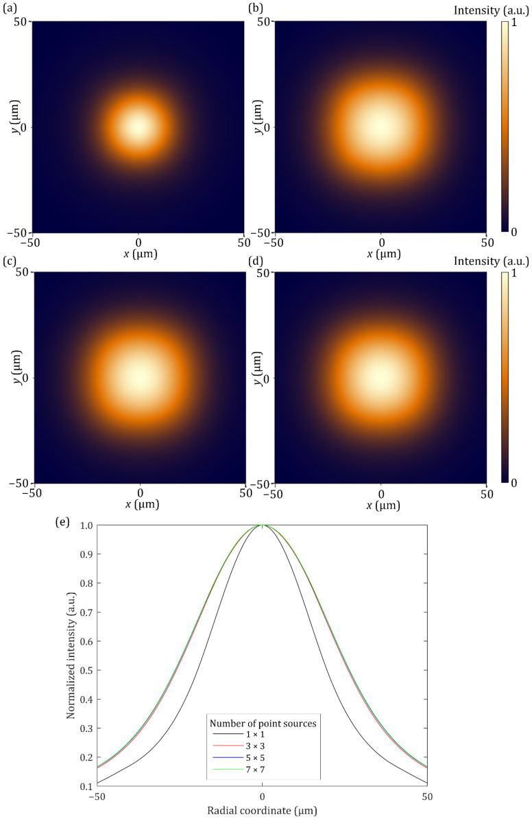
The LEDs are described as numerous point sources with Lambertian intensity profiles that are incoherently summed. Thus, the designed LED source is an incoherent, unpolarized, surface light source. A 35 μm square LED source is used in this study. A micro-LED chip can be considered as a point source [82]. Figure 1 shows the simulated results after 20 μm of propagation with different numbers of points sources. The intensity profiles converge as the number of points sources become 3 × 3. In addition, the optimized and required chip size is at least 7 μm for typical display panels, including smartphones, laptops, and televisions [83,84,85], so 5 × 5 and 7 × 7 micro-chips are not considered in this study. We consider the LED source composed of 3 × 3 micro-LED chips, and the light source is described by 3 × 3 points sources. Because the light emitted from the LED is partially spatial-coherent, the phase of light originating from each point source is random and therefore interference effects are ignored. The propagation results shown in Figure 1 are obtained by adding only the amplitudes of the propagated light.
Figure 1.
Simulated results after 20 μm of propagation with different numbers of points sources: (a) 1 × 1; (b) 3 × 3; (c) 5 × 5; (d) 7 × 7; (e) Intensity profiles. The results converge as the number of the point sources becomes 3 × 3.
The Lambertian intensity profile is expressed as [86]
| (1) |
where I is the intensity, θ is the propagation angle with respect to the optical axis, and I0 is the maximum intensity at θ = 0, respectively. To describe the Lambertian point source, an interface between two different media is used (Figure S1). Because the transmittance at the interface is dependent on θ, the intensity of the transmitted light also varies with θ. When the distance between the point source and the interface is 40 nm and the refractive indices of the media are 1 and 2, the intensity profile of the transmitted light is similar to a Lambertian intensity profile, therefore allowing us to describe the single point source. The LED source is then modeled as 3 × 3 point sources placed 40 nm away from the interface. The schematics of the simulation is shown in Figure S2. Figure S3 shows the difference when a single point source and 3 × 3 points sources are used. However, individual simulations are done for each point source as the LED source is partially spatial-coherent, and therefore interference must be neglected [87]. The final calculations result from the incoherent summation of each individual simulation. The total number of simulations can be reduced if the system is symmetrically designed, allowing some results to be obtained by rotating other results. In addition, the partial temporal coherence of the LED source provides a broad spectral bandwidth of emitted light [88]. The simulation results with both narrowband and broadband sources provide similar results (Figure S4); therefore, the effect of the partial temporal coherence is negligible and ignored.
In this work, the points sources are placed at the center of the 3 × 3 lattice (Figure S2b). The effect of the relative locations of the sources is negligible in a 3 μm × 3 μm LED source, as the 3 × 3 array of dipole sources provides a similar light emission to a single point source of the same size [89].
2.2. Phase Profile of Metalens
The typical phase profile φt of an ML is expressed as [50]
| (2) |
where r, λ, and f are the radial coordinate, the wavelength, and the focal length, respectively. Spherical waves from the LED source are transmitted through the ML and collimated. However, the collimated light is concentrated at the propagation angle of 0°, so the phase profile is modified to enhance the luminous intensity within the detection angle of 10°. The modified phase profile φm is expressed as
| (3) |
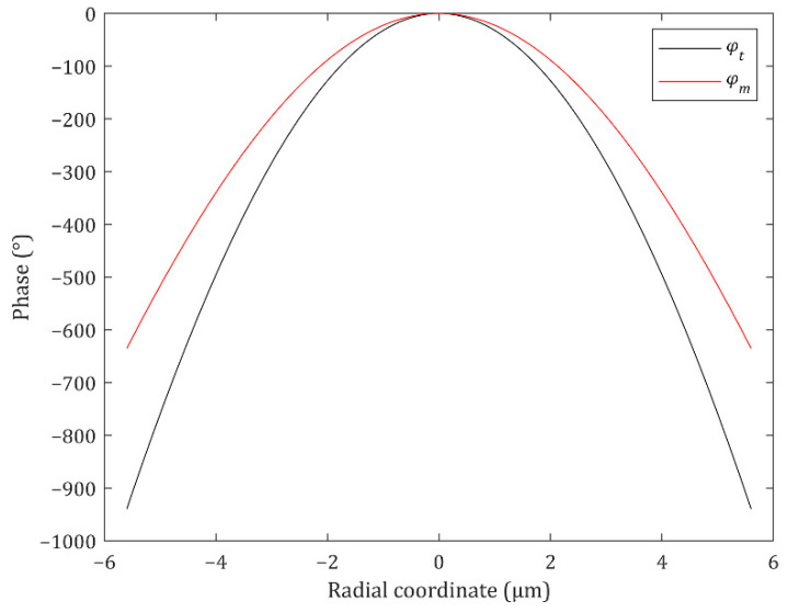
where L is the length of the ML, m is the number of point sources that make up of the LED source, and α is the detection angle. L is 35 μm, the same with the length of the LED source, m is 3 because 3 × 3 points sources are used, and α is 10° in this study. Because the lengths of the ML and the LED are identical, an ML array can be used to cover a large-area LED composed of equally sized LED pixels. The phase profile from Equation (3) is obtained by adding the phase profiles of the typical ML (Equation (2)) and a concave lens (Figure S5). The second term of Equation (3) originates from the concave lens allowing the transmitted light to spread out to the target detection angle region. Because the LED source is a surface light source and is described as a set of the points sources, the designed ML is split into the subsections one-to-one correspondence with the point sources and the phase profile in each subsection is defined by Equation (2) or (3). The phase profiles at f = 10 μm and λ = 560 nm are shown in Figure 2. The phase gradient of φm becomes smaller at the edge of the ML than that of φt. Thus, when φm is used, the diverging light from the source is steered less and spreads out to the target detection angle region.
Figure 2.
The typical (black line) and modified (red line) phase profiles of the metalens (ML) at f = 10 μm and λ = 560 nm.
2.3. Nanohole Meta-Atom
Since LEDs emit unpolarized light, polarization-insensitive meta-atoms are designed. In addition, nanohole meta-atoms are used instead of nanofins due to good adhesion between the nanohole structure and the substrate when the high aspect ratio (above 1:5) nanostructures are fabricated (Figure S6). Because the dense material is continuously connected, the nanohole structure provides a high production yield. However, the nanofin structure can be relatively easily destroyed during the etching or cleaning process. When the optical axis of the system is parallel to the z-direction, the transmitted electric field through the nanohole is expressed as [50,90,91,92]
| (4) |
where tl and ts are complex transmission coefficients when the incident light is polarized along the long and short axis of the nanohole, respectively, and β is the rotation angle of the nanohole with respect to the x-axis. The first and the second terms of Equation (4) are known as the co- and cross-polarization terms, respectively, because the Jones vector of each term shows that the polarization of the transmitted light is identical to the incident light at the first term and is opposite the incident light at the second term. The polarization dependence is caused by exp(±i2β) from the cross-polarization term. Therefore, the meta-atoms are designed to have the same tl and ts to remove the cross-polarization term, which can be achieved using symmetrical meta-atoms such as circle and square holes (Figure S7).
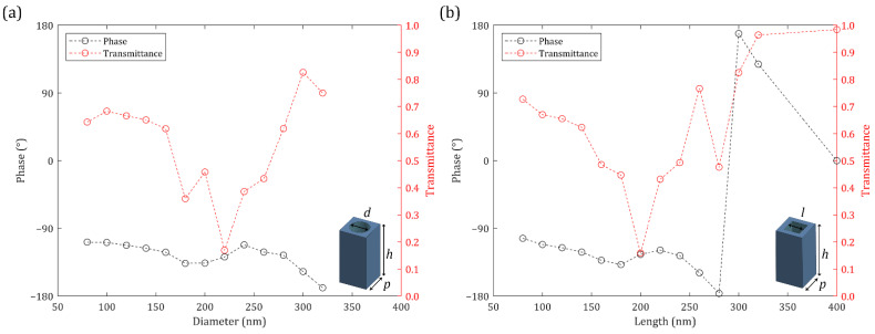
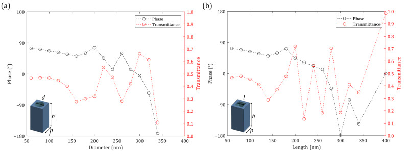
Titanium dioxide (TiO2) and amorphous silicon (a-Si) nanohole meta-atoms are usually used at visible frequencies due to their high refractive indices and low loss [93]. Gallium nitride (GaN) has also been used at visible frequencies; however, a sapphire substrate is required and the sapphire substrate is less transparent than fused silica [49]. Thus, TiO2 and a-Si are used in this study. The transmission properties of TiO2 nanohole meta-atoms with a height of 400 nm are investigated using rigorous coupled-wave analysis (RCWA) simulations (Figure 3) [94]. The designed meta-atoms work under the spherical wave incidence even though they are designed by RCWA under the plane wave incidence (Figure S8). The phase shown in Figure 3 does not satisfy the complete 2π coverage. However, they can be used to construct an ML even though the meta-atom library does not fully cover the phase from −π to π [54]. Meanwhile, the transmission properties of a-Si nanohole meta-atoms with height of 600 nm are also calculated using RCWA simulations (Figure 4). The fabrication process for a-Si meta atoms is relatively easier and is less restrictive than that of TiO2 meta-atoms, so a-Si meta-atoms can be designed with higher aspect ratios. Nevertheless, the phase depicted in Figure 4 does not cover the entire 2π range. The averaged transmittance of a-Si meta-atoms is lower than that of TiO2 meta-atoms.
Figure 3.
Transmission properties of Titanium dioxide (TiO2) meta-atoms at λ = 560 nm: (a) Circle nanohole meta-atoms; (b) Square nanohole meta-atoms. p = 400 nm and h = 400 nm.
Figure 4.
Transmission properties of amorphous silicon (a-Si) meta-atoms at λ = 560 nm: (a) Circle nanohole meta-atoms; (b) Square nanohole meta-atoms. p = 400 nm and h = 600 nm.
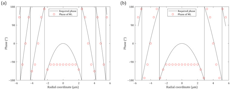
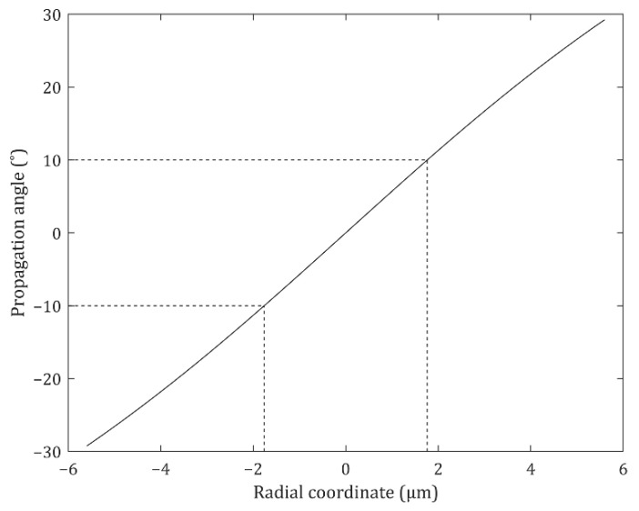
Figure 5 shows the phases of the designed TiO2 MLs. The phase profile at the center of the lens is somewhat different from the desired phases. However, the θ of light at the center is already below 10° (Figure 6) and is smaller than 10° at r < 1.76 μm. Thus, the transmitted light can reach the target detection angle region regardless of the zero phase gradient at the center. The MLs should steer the incident light at the edge to enhance the intensity within the target detection angle of 10°. Therefore, beam control at the edge is enough to construct the MLs, and the phase modulation at the edge is important for these designs.
Figure 5.
Comparisons of the required (black line) and the designed (red dot) phase of the MLs at f = 10 μm and λ = 560 nm: (a) The TiO2 ML with the typical phase profile; (b) The TiO2 ML with the modified phase profile.
Figure 6.
Propagation angle of the emitted light from the light-emitting diode (LED) source. Because the propagation angle at r < 1.76 μm is already below the target detection angle 10°, the phase modulation at the edge is enough to construct the MLs.
2.4. Far Field Propagation Simulation
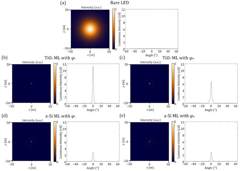
The diverging spherical wave from the LED source passes through the ML and is able to propagate to the far field as the ML collimates the transmitted light. The emitted light from the LED source is at a distance f from the ML, then propagates for 25 m. The simulated propagation results are shown in Figure 7. The luminous intensities are calculated. Each ML enhances the luminous intensity at the center and the luminous intensity profile shows the peak near the angle of 0°. The peaks of the MLs with φt at the center are higher but narrower than the MLs with φm regardless of the materials. Because the cross-sectional intensity profiles shown in Figure 7 are radially symmetric, the intensity at large angles are more dominant to enhance the total luminous intensity. Table 1 shows the luminous intensities of the MLs with respect to the angle from 0° (center) to 10° (target detection angle). The MLs with φm have larger luminous intensities, except at the angle of 0°, than that of the MLs with φt for both materials. In addition, full widths at half maximum of the TiO2 MLs with φt and φm after 25 m of propagation are 1.22 and 1.45 m, respectively, and the full widths at half maximum of the a-Si MLs with φt and φm are 1.24, and 1.26 m, respectively.
Figure 7.
Simulated results after 25 m propagation with respect to the propagation angle θ: (a) The bare LED without any ML; (b) The TiO2 ML with the typical phase profile; (c) The TiO2 ML with the modified phase profile; (d) The a-Si ML with the typical phase profile; (e) The a-Si ML with the modified phase profile. The MLs with the modified phase profile provide lower but wider intensity profiles than those of the MLs with the typical phase profile.
Table 1.
Luminous intensity of MLs at different propagation angles θ. Unit: cd.
| Propagation Angle (θ) | |||||
|---|---|---|---|---|---|
| 0° | 2.5° | 5° | 7.5° | 10° | |
| Without ML (bare LED) | 0.1315 | 0.1301 | 0.1297 | 0.1290 | 0.1271 |
| TiO2 ML with φt | 11.37 | 1.107 | 0.1228 | 0.2157 | 0.05475 |
| TiO2 ML with φm | 6.668 | 1.562 | 0.7678 | 0.1265 | 0.1720 |
| a-Si ML with φt | 2.912 | 0.3451 | 0.1022 | 0.06574 | 0.08123 |
| a-Si ML with φm | 2.778 | 0.4787 | 0.1306 | 0.1454 | 0.03788 |
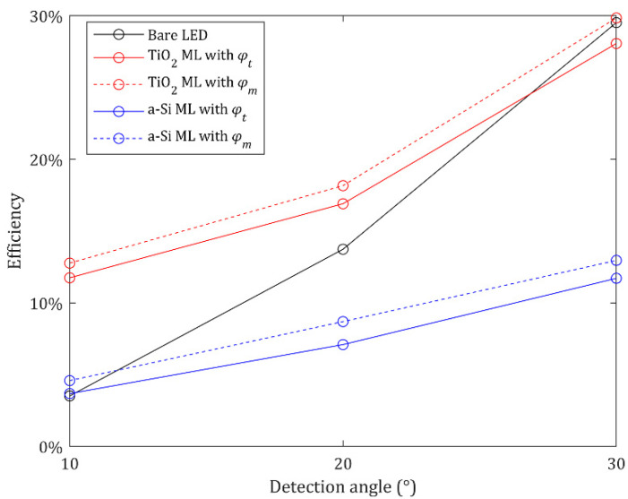
The MLs enhance the peak intensity by steering the direction of the transmitted light but do not increase the light extraction efficiency of the LED. In addition, some portion of light is reflected or absorbed by the MLs. Therefore, the enhancement of the luminous intensity at the center implies that the intensity at the other areas decreases. The efficiencies of the MLs are shown in Figure 8 with respect to α. The efficiency is defined as the output luminous intensity within α (Figure S9) divided by the luminous intensity of the LED source. The TiO2 ML with φm has higher efficiencies within α = 10°, 20°, and 30° than those of the bare LED, but the ML with φt has lower efficiency within α = 30°. The luminous intensity within α = 10° is enhanced by 234% and 263% compared with the LED source when the TiO2 MLs with φt and φm are used, respectively (Table S1). Because the ML with φm has the wide intensity peak profile, the ML has a higher luminous intensity within α = 10° than that of the ML with φt despite the lower maximum luminous intensity at the center. Meanwhile, the enhancement of the luminous intensity within α = 20° and 30° is not significant, because the enhancement within α = 10° is a consequence of steering the transmitted light from the other area to the target detection angle region. The a-Si ML with φm provides the higher efficiencies within α = 10°, 20°, and 30° than those of the a-Si ML with φt due to the wider intensity profile. However, the a-Si MLs enhance the efficiencies slightly within α = 10° and have lower efficiencies within α = 20° and 30° due to the low transmittance of a-Si meta-atoms.
Figure 8.
Efficiencies of the LED source and MLs within the different detection angles α.
3. Conclusions
The MLs are designed to enhance the luminous intensity of incoherent LED sources after 25 m of propagation within α = 0° and 10°. The LED source is composed of 3 × 3 micro-chips and is designed as the set of 3 × 3 Lambertian point sources. The propagation results are obtained by incoherently adding the simulation result with each single point source. Polarization-insensitive nanohole meta-atoms are designed. Although the phase profiles of the designed MLs do not match with the required phases at the center, the emitted light from the LED source at the center already propagates in the target detection angle region, so the phase modulation at the edge of the MLs is important in this study. When the TiO2 and a-Si MLs with φt are used, the luminous intensity at the center is enhanced by 8551% and 2115%, respectively. Meanwhile, the TiO2 and a-Si MLs with φm enhance the luminous intensity within α = 10° by 263% and 30%, respectively. Because the TiO2 meta-atoms have higher transmittance than that of a-Si, the TiO2 ML shows the higher enhancement. Meanwhile, the efficiency enhancement within α = 20° or 30° is not significant because the ML cannot increase the light extraction efficiency of the LED source and the enhancement within α = 0° or 10° is a consequence of steering the transmitted light. Therefore, the emitted light from the LED source can be delivered over a long distance using the ML, proving that it can be employed for various practical applications using LEDs, including the automotive headlights, display panels and so on.
4. Methods
Commercially available Lumerical FDTD and VirtualLab Fusion were used for the far field simulations. The electric field transmitted through the ML was calculated using Lumerical FDTD. Then the electric field data were imported to VirtualLab Fusion and used as the source for the far field propagation. Finally, the simulated far field propagation results from each individual point source were incoherently summed up.
Supplementary Materials
The following are available online at https://www.mdpi.com/article/10.3390/nano12010153/s1, Figure S1: Description of a point source with Lambertian intensity profile: (a) Schematics; (b) The Lambertian (black line) and simulated (red line) intensity profiles; Figure S2: Schematics of the simulation in this work: (a) The simulation from the LED source to the monitor is carried out using Lumerical FDTD. The far field simulation from the monitor to the detector is conducted using VirtualLab Fusion; (b) Distribution of the 3 × 3 points sources; Figure S3: Comparisons of the simulated results calculated from a single point source and 3 × 3 points sources; Figure S4: Comparisons of the simulated results with a narrowband source at λ = 560 nm and broadband source at 500 ≤ λ ≤ 620 nm; Figure S5: Description of the effect of the ML with φm explained by geometrical optics; Figure S6: Good adhesion of nanohole meta-atoms: (a) a-Si nanostructure composed of nanofin meta-atoms; (b) a-Si nanostructure composed of nanohole meta-atoms. Scale bar: 1 μm; Figure S7. Comparison of tl (solid line) and ts (circle dot) of TiO2 meta-atoms: (a) Circle nanohole meta-atoms; (b) Square nanohole meta-atoms; Figure S8: Simulation result of the collimation using the TiO2 ML with φt. The focal length is 3 μm. The phase is plotted instead of the intensity, because the intensity at the point source is extremely larger than that at the other area; Figure S9: Measurement of the intensity within a detection angle of α. α = 0° or 10° and l = 25 m; Table S1: Comparison of enhancement of intensity from LED sources of the previously reported results.
Author Contributions
Conceptualization, J.R.; methodology, H.C., H.J., Y.Y. and J.R.; software, H.C.; validation, H.C.; formal analysis, H.C.; data curation, H.C.; writing—original draft preparation, H.C., H.J.; writing—review and editing, H.C., H.J., Y.Y., T.B. and J.R.; visualization, H.C., H.J., Y.Y. and T.B.; supervision, J.R.; project administration, J.R.; funding acquisition, J.R. All authors have read and agreed to the published version of the manuscript.
Funding
This work was financially supported by the POSCO-POSTECH-RIST Convergence Research Center program funded by POSCO, an industry-university strategic grant funded by SL Corporation, and the National Research Foundation (NRF) grants (NRF-2019R1A2C3003129, CAMM-2019M3A6B3030637, NRF-2019R1A5A8080290) funded by the Ministry of Science and ICT of the Korean government. Y.Y. acknowledges the Hyundai Motor Chung Mong-Koo fellowship, and the NRF fellowship (NRF-2021R1A6A3A13038935) funded by the Ministry of Education of the Korean government.
Institutional Review Board Statement
Not applicable.
Informed Consent Statement
Not applicable.
Data Availability Statement
The data presented in this study are available on request from the corresponding author.
Conflicts of Interest
The authors declare no conflict of interest.
Footnotes
Publisher’s Note: MDPI stays neutral with regard to jurisdictional claims in published maps and institutional affiliations.
References
- 1.Yu N., Capasso F. Flat optics with designer metasurfaces. Nat. Mater. 2014;13:139–150. doi: 10.1038/nmat3839. [DOI] [PubMed] [Google Scholar]
- 2.Dolling G., Enkrich C., Wegener M., Soukoulis C.M., Linden S. Simultaneous negative phase and group velocity of light in a metamaterial. Science. 2006;312:892–894. doi: 10.1126/science.1126021. [DOI] [PubMed] [Google Scholar]
- 3.Kristensen A., Yang J.K.W., Bozhevolnyi S.I., Link S., Nordlander P., Halas N.J., Mortensen N.A. Plasmonic colour generation. Nat. Rev. Mater. 2016;2:16088. doi: 10.1038/natrevmats.2016.88. [DOI] [Google Scholar]
- 4.Lee T., Jang J., Jeong H., Rho J. Plasmonic- and dielectric-based structural coloring: From fundamentals to practical applications. Nano Converg. 2018;5:1. doi: 10.1186/s40580-017-0133-y. [DOI] [PMC free article] [PubMed] [Google Scholar]
- 5.Badloe T., Mun J., Rho J. Metasurfaces-Based Absorption and Reflection Control: Perfect Absorbers and Reflectors. J. Nanomater. 2017;2017:2361042. doi: 10.1155/2017/2361042. [DOI] [Google Scholar]
- 6.Hao J., Yuan Y., Ran L., Jiang T., Kong J.A., Chan C.T., Zhou L. Manipulating electromagnetic wave polarizations by anisotropic metamaterials. Phys. Rev. Lett. 2007;99:063908. doi: 10.1103/PhysRevLett.99.063908. [DOI] [PubMed] [Google Scholar]
- 7.Yoon G., Lee D., Nam K.T., Rho J. Geometric metasurface enabling polarization independent beam splitting. Sci. Rep. 2018;8:9468. doi: 10.1038/s41598-018-27876-2. [DOI] [PMC free article] [PubMed] [Google Scholar]
- 8.Khorasaninejad M., Chen W.T., Devlin R.C., Oh J., Zhu A.Y., Capasso F. Metalenses at visible wavelengths: Diffraction-limited focusing and subwavelength resolution imaging. Science. 2016;352:1190–1194. doi: 10.1126/science.aaf6644. [DOI] [PubMed] [Google Scholar]
- 9.Lee D., Gwak J., Badloe T., Palomba S., Rho J. Metasurfaces-based imaging and applications: From miniaturized optical components to functional imaging platforms. Nanoscale Adv. 2020;2:605–625. doi: 10.1039/C9NA00751B. [DOI] [PMC free article] [PubMed] [Google Scholar]
- 10.Moon S.W., Kim Y., Yoon G., Rho J. Recent Progress on Ultrathin Metalenses for Flat Optics. iScience. 2020;23:101877. doi: 10.1016/j.isci.2020.101877. [DOI] [PMC free article] [PubMed] [Google Scholar]
- 11.Lee T., Lee C., Oh D.K., Badloe T., Ok J.G., Rho J. Scalable and high-throughput top-down manufacturing of optical metasurfaces. Sensors. 2020;20:4108. doi: 10.3390/s20154108. [DOI] [PMC free article] [PubMed] [Google Scholar]
- 12.Kim M., Rho J. Metamaterials and imaging. Nano Converg. 2015;2:22. doi: 10.1186/s40580-015-0053-7. [DOI] [PMC free article] [PubMed] [Google Scholar]
- 13.Yoon G., Tanaka T., Zentgraf T., Rho J. Recent progress on metasurfaces: Applications and fabrication. J. Phys. D Appl. Phys. 2021;54:383002. doi: 10.1088/1361-6463/ac0faa. [DOI] [Google Scholar]
- 14.Jung C., Kim G., Jeong M., Jang J., Dong Z., Badloe T., Yang J.K.W., Rho J. Metasurface-Driven Optically Variable Devices. Chem. Rev. 2021;121:13013–13050. doi: 10.1021/acs.chemrev.1c00294. [DOI] [PubMed] [Google Scholar]
- 15.Ansari M.A., Kim I., Lee D., Waseem M.H., Zubair M., Mahmood N., Badloe T., Yerci S., Tauqeer T., Mehmood M.Q., et al. A Spin-Encoded All-Dielectric Metahologram for Visible Light. Laser Photonics Rev. 2019;13:1900065. doi: 10.1002/lpor.201900065. [DOI] [Google Scholar]
- 16.Naveed M.A., Ansari M.A., Kim I., Badloe T., Kim J., Oh D.K., Riaz K., Tauqeer T., Younis U., Saleem M., et al. Optical spin-symmetry breaking for high-efficiency directional helicity-multiplexed metaholograms. Microsyst. Nanoeng. 2021;7:5. doi: 10.1038/s41378-020-00226-x. [DOI] [PMC free article] [PubMed] [Google Scholar]
- 17.Yoon G., Lee D., Nam K.T., Rho J. Pragmatic Metasurface Hologram at Visible Wavelength: The Balance between Diffraction Efficiency and Fabrication Compatibility. ACS Photonics. 2018;5:1643–1647. doi: 10.1021/acsphotonics.7b01044. [DOI] [Google Scholar]
- 18.Kim I., Ansari M.A., Mehmood M.Q., Kim W.S., Jang J., Zubair M., Kim Y.K., Rho J. Stimuli-Responsive Dynamic Metaholographic Displays with Designer Liquid Crystal Modulators. Adv. Mater. 2020;32:2004664. doi: 10.1002/adma.202004664. [DOI] [PubMed] [Google Scholar]
- 19.Ansari M.A., Kim I., Rukhlenko I.D., Zubair M., Yerci S., Tauqeer T., Mehmood M.Q., Rho J. Engineering spin and antiferromagnetic resonances to realize an efficient direction-multiplexed visible meta-hologram. Nanoscale Horiz. 2019 doi: 10.1039/C9NH00460B. [DOI] [Google Scholar]
- 20.Li X., Ren H., Chen X., Liu J., Li Q., Li C., Xue G., Jia J., Cao L., Sahu A., et al. Athermally photoreduced graphene oxides for three-dimensional holographic images. Nat. Commun. 2015;6:6984. doi: 10.1038/ncomms7984. [DOI] [PMC free article] [PubMed] [Google Scholar]
- 21.Yoon G., Lee D., Nam K.T., Rho J. “Crypto-Display” in Dual-Mode Metasurfaces by Simultaneous Control of Phase and Spectral Responses. ACS Nano. 2018;12:6421–6428. doi: 10.1021/acsnano.8b01344. [DOI] [PubMed] [Google Scholar]
- 22.Lee G.-Y., Yoon G., Lee S.-Y., Yun H., Cho J., Lee K., Kim H., Rho J., Lee B. Complete amplitude and phase control of light using broadband holographic metasurfaces. Nanoscale. 2018;10:4237–4245. doi: 10.1039/C7NR07154J. [DOI] [PubMed] [Google Scholar]
- 23.Zheng G., Mühlenbernd H., Kenney M., Li G., Zentgraf T., Zhang S. Metasurface holograms reaching 80% efficiency. Nat. Nanotechnol. 2015;10:308. doi: 10.1038/nnano.2015.2. [DOI] [PubMed] [Google Scholar]
- 24.Zhou Y., Kravchenko I.I., Wang H., Zheng H., Gu G., Valentine J. Multifunctional metaoptics based on bilayer metasurfaces. Light Sci. Appl. 2019;8:80. doi: 10.1038/s41377-019-0193-3. [DOI] [PMC free article] [PubMed] [Google Scholar]
- 25.Kim I., Jang J., Kim G., Lee J., Badloe T., Mun J., Rho J. Pixelated bifunctional metasurface-driven dynamic vectorial holographic color prints for photonic security platform. Nat. Commun. 2021;12:3614. doi: 10.1038/s41467-021-23814-5. [DOI] [PMC free article] [PubMed] [Google Scholar]
- 26.Ren H., Fang X., Jang J., Bürger J., Rho J., Maier S.A. Complex-amplitude metasurface-based orbital angular momentum holography in momentum space. Nat. Nanotechnol. 2020;15:948–955. doi: 10.1038/s41565-020-0768-4. [DOI] [PubMed] [Google Scholar]
- 27.Kim I., Yoon G., Jang J., Genevet P., Nam K.T., Rho J. Outfitting Next Generation Displays with Optical Metasurfaces. ACS Photonics. 2018;5:3876–3895. doi: 10.1021/acsphotonics.8b00809. [DOI] [Google Scholar]
- 28.Jang J., Jeong H., Hu G., Qiu C.-W., Nam K.T., Rho J. Kerker-Conditioned Dynamic Cryptographic Nanoprints. Adv. Opt. Mater. 2019;7:1801070. doi: 10.1002/adom.201970016. [DOI] [Google Scholar]
- 29.Tseng M.L., Yang J., Semmlinger M., Zhang C., Nordlander P., Halas N.J. Two-Dimensional Active Tuning of an Aluminum Plasmonic Array for Full-Spectrum Response. Nano Lett. 2017;17:6034–6039. doi: 10.1021/acs.nanolett.7b02350. [DOI] [PubMed] [Google Scholar]
- 30.Yang B., Liu W., Li Z., Cheng H., Choi D.-Y., Chen S., Tian J. Ultrahighly Saturated Structural Colors Enhanced by Multipolar-Modulated Metasurfaces. Nano Lett. 2019;19:4221–4228. doi: 10.1021/acs.nanolett.8b04923. [DOI] [PubMed] [Google Scholar]
- 31.Jang J., Badloe T., Yang Y., Lee T., Mun J., Rho J. Spectral modulation through the hybridization of Mie-scatterers and quasi-guided mode resonances: Realizing full and gradients of structural color. ACS Nano. 2020;14:15317–15326. doi: 10.1021/acsnano.0c05656. [DOI] [PubMed] [Google Scholar]
- 32.Wu P.C., Pala R.A., Kafaie Shirmanesh G., Cheng W.H., Sokhoyan R., Grajower M., Alam M.Z., Lee D., Atwater H.A. Dynamic beam steering with all-dielectric electro-optic III–V multiple-quantum-well metasurfaces. Nat. Commun. 2019;10:3654. doi: 10.1038/s41467-019-11598-8. [DOI] [PMC free article] [PubMed] [Google Scholar]
- 33.Holsteen A.L., Cihan A.F., Brongersma M.L. Temporal color mixing and dynamic beam shaping with silicon metasurfaces. Science. 2019;365:257–260. doi: 10.1126/science.aax5961. [DOI] [PubMed] [Google Scholar]
- 34.Wang L., Ng R.J.H., Safari Dinachali S., Jalali M., Yu Y., Yang J.K.W. Large Area Plasmonic Color Palettes with Expanded Gamut Using Colloidal Self-Assembly. ACS Photonics. 2016;3:627–633. doi: 10.1021/acsphotonics.5b00725. [DOI] [Google Scholar]
- 35.Li Z., Dai Q., Mehmood M.Q., Hu G., Yanchuk B.L., Tao J., Hao C., Kim I., Jeong H., Zheng G., et al. Full-space Cloud of Random Points with a Scrambling Metasurface. Light Sci. Appl. 2018;7:63. doi: 10.1038/s41377-018-0064-3. [DOI] [PMC free article] [PubMed] [Google Scholar]
- 36.Xie Y.Y., Ni P.N., Wang Q.H., Kan Q., Briere G., Chen P.P., Zhao Z.Z., Delga A., Ren H.R., Da Chen H., et al. Metasurface-integrated vertical cavity surface-emitting lasers for programmable directional lasing emissions. Nat. Nanotechnol. 2020;15:125–130. doi: 10.1038/s41565-019-0611-y. [DOI] [PubMed] [Google Scholar]
- 37.Kim I., Martins R.J., Jang J., Badloe T., Khadir S., Jung H.Y., Kim H., Kim J., Genevet P., Rho J. Nanophotonics for light detection and ranging technology. Nat. Nanotechnol. 2021;16:508–524. doi: 10.1038/s41565-021-00895-3. [DOI] [PubMed] [Google Scholar]
- 38.Lee C.W., Choi H.J., Jeong H. Tunable metasurfaces for visible and SWIR applications. Nano Converg. 2020;7:18. doi: 10.1186/s40580-019-0213-2. [DOI] [PMC free article] [PubMed] [Google Scholar]
- 39.Yao Y., Shankar R., Kats M.A., Song Y., Kong J., Loncar M., Capasso F. Electrically tunable metasurface perfect absorbers for ultrathin mid-infrared optical modulators. Nano Lett. 2014;14:6526–6532. doi: 10.1021/nl503104n. [DOI] [PubMed] [Google Scholar]
- 40.Yoon G., So S., Kim M., Mun J., Ma R., Rho J. Electrically tunable metasurface perfect absorber for infrared frequencies. Nano Converg. 2017;4:36. doi: 10.1186/s40580-017-0131-0. [DOI] [PMC free article] [PubMed] [Google Scholar]
- 41.Zhao Y., Askarpour A.N., Sun L., Shi J., Li X., Alu A. Chirality detection of enantiomers using twisted optical metamaterials. Nat. Commun. 2017;8:14180. doi: 10.1038/ncomms14180. [DOI] [PMC free article] [PubMed] [Google Scholar]
- 42.Jang J., Kang K., Raeis-Hosseini N., Ismukhanova A., Jeong H., Jung C., Kim B., Lee J.Y., Park I., Rho J. Self-Powered Humidity Sensor Using Chitosan-Based Plasmonic Metal–Hydrogel–Metal Filters. Adv. Opt. Mater. 2020;8:1901932. doi: 10.1002/adom.201901932. [DOI] [Google Scholar]
- 43.Yang Y., Lee T., Kim M., Jung C., Badloe T., Lee D., Lee S., Lee H.J., Rho J. Dynamic Optical Spin Hall Effect in Chitosan-Coated All-Dielectric Metamaterials for a Biosensing Platform. IEEE J. Sel. Top. Quantum Electron. 2021;27:7300608. doi: 10.1109/JSTQE.2021.3065826. [DOI] [Google Scholar]
- 44.Seo M.H., Kang K., Yoo J.Y., Park J., Lee J.S., Cho I., Kim B.J., Jeong Y., Lee J.Y., Kim B., et al. Chemo-Mechanically Operating Palladium-Polymer Nanograting Film for a Self-Powered H2 Gas Sensor. ACS Nano. 2020;14:16813–16822. doi: 10.1021/acsnano.0c05476. [DOI] [PubMed] [Google Scholar]
- 45.Kim I., Kim W.S., Kim K., Ansari M.A., Mehmood M.Q., Badloe T., Kim Y., Gwak J., Lee H., Kim Y.K., et al. Holographic metasurface gas sensors for instantaneous visual alarms. Sci. Adv. 2021;7:eabe9943. doi: 10.1126/sciadv.abe9943. [DOI] [PMC free article] [PubMed] [Google Scholar]
- 46.Kim J., Rana A.S., Kim Y., Kim I., Badloe T., Zubair M., Mehmood M.Q., Rho J. Chiroptical Metasurfaces: Principles, Classification, and Applications. Sensors. 2021;21:4381. doi: 10.3390/s21134381. [DOI] [PMC free article] [PubMed] [Google Scholar]
- 47.Park Y.M., Lim S.Y., Jeong S.W., Song Y., Bae N.H., Hong S.B., Choi B.G., Lee S.J., Lee K.G. Flexible nanopillar-based electrochemical sensors for genetic detection of foodborne pathogens. Nano Converg. 2018;5:15. doi: 10.1186/s40580-018-0147-0. [DOI] [PMC free article] [PubMed] [Google Scholar]
- 48.Chen W.T., Zhu A.Y., Sanjeev V., Khorasaninejad M., Shi Z., Lee E., Capasso F. A broadband achromatic metalens for focusing and imaging in the visible. Nat. Nanotechnol. 2018;13:220–226. doi: 10.1038/s41565-017-0034-6. [DOI] [PubMed] [Google Scholar]
- 49.Wang S., Wu P.C., Su V.C., Lai Y.C., Chen M.K., Kuo H.Y., Chen B.H., Chen Y.H., Huang T.T., Wang J.H., et al. A broadband achromatic metalens in the visible. Nat. Nanotechnol. 2018;13:227–232. doi: 10.1038/s41565-017-0052-4. [DOI] [PubMed] [Google Scholar]
- 50.Chen W.T., Zhu A.Y., Sisler J., Bharwani Z., Capasso F. A broadband achromatic polarization-insensitive metalens consisting of anisotropic nanostructures. Nat. Commun. 2019;10:355. doi: 10.1038/s41467-019-08305-y. [DOI] [PMC free article] [PubMed] [Google Scholar]
- 51.Khorasaninejad M., Zhu A.Y., Roques-Carmes C., Chen W.T., Oh J., Mishra I., Devlin R.C., Capasso F. Polarization-Insensitive Metalenses at Visible Wavelengths. Nano Lett. 2016;16:7229–7234. doi: 10.1021/acs.nanolett.6b03626. [DOI] [PubMed] [Google Scholar]
- 52.Shalaginov M.Y., An S., Yang F., Su P., Lyzwa D., Agarwal A.M., Zhang H., Hu J., Gu T. Single-Element Diffraction-Limited Fisheye Metalens. Nano Lett. 2020;20:7429–7437. doi: 10.1021/acs.nanolett.0c02783. [DOI] [PubMed] [Google Scholar]
- 53.Groever B., Chen W.T., Capasso F. Meta-lens doublet in the visible region. Nano Lett. 2017;17:4902–4907. doi: 10.1021/acs.nanolett.7b01888. [DOI] [PubMed] [Google Scholar]
- 54.Park J.S., Zhang S., She A., Chen W.T., Lin P., Yousef K.M.A., Cheng J.X., Capasso F. All-Glass, Large Metalens at Visible Wavelength Using Deep-Ultraviolet Projection Lithography. Nano Lett. 2019;19:8673–8682. doi: 10.1021/acs.nanolett.9b03333. [DOI] [PubMed] [Google Scholar]
- 55.Li Z., Lin P., Huang Y.W., Park J.S., Chen W.T., Shi Z., Qiu C.W., Cheng J.X., Capasso F. Meta-optics achieves RGB-achromatic focusing for virtual reality. Sci. Adv. 2021;7:eabe4458. doi: 10.1126/sciadv.abe4458. [DOI] [PMC free article] [PubMed] [Google Scholar]
- 56.Lee G.Y., Hong J.Y., Hwang S., Moon S., Kang H., Jeon S., Kim H., Jeong J.H., Lee B. Metasurface eyepiece for augmented reality. Nat. Commun. 2018;9:4562. doi: 10.1038/s41467-018-07011-5. [DOI] [PMC free article] [PubMed] [Google Scholar]
- 57.Badloe T., Kim I., Kim Y., Kim J., Rho J. Electrically Tunable Bifocal Metalens with Diffraction-Limited Focusing and Imaging at Visible Wavelengths. Adv. Sci. 2021;8:2102646. doi: 10.1002/advs.202102646. [DOI] [PMC free article] [PubMed] [Google Scholar]
- 58.Badloe T., Lee J., Seong J., Rho J. Tunable Metasurfaces: The Path to Fully Active Nanophotonics. Adv. Photonics Res. 2021;2:2000205. doi: 10.1002/adpr.202000205. [DOI] [Google Scholar]
- 59.Chen Y., Ai B., Wong Z.J. Soft optical metamaterials. Nano Converg. 2020;7:18. doi: 10.1186/s40580-020-00226-7. [DOI] [PMC free article] [PubMed] [Google Scholar]
- 60.Yoon G., Kim K., Huh D., Lee H., Rho J. Single-step manufacturing of hierarchical dielectric metalens in the visible. Nat. Commun. 2020;11:2268. doi: 10.1038/s41467-020-16136-5. [DOI] [PMC free article] [PubMed] [Google Scholar]
- 61.Yoon G., Kim K., Kim S.-U., Han S., Lee H., Rho J. Printable Nanocomposite Metalens for High-Contrast Near-Infrared Imaging. ACS Nano. 2021;15:698–706. doi: 10.1021/acsnano.0c06968. [DOI] [PubMed] [Google Scholar]
- 62.Jeong H., Yang Y., Cho H., Badloe T., Kim I., Ma R.M., Rho J. Emerging advanced metasurfaces: Alternatives to conventional bulk optical devices. Microelectron. Eng. 2020;220:111146. doi: 10.1016/j.mee.2019.111146. [DOI] [Google Scholar]
- 63.Na J.-Y., Yoon S.-S., Kim Y.-B., Kim S.-K. Integrated ray-wave optics modeling for macroscopic diffractive lighting devices. Opt. Express. 2019;27:37910. doi: 10.1364/OE.27.037910. [DOI] [PubMed] [Google Scholar]
- 64.Karthaus D., Giehl M., Sandfuchs O., Sinzinger S. Modeling of light-emitting diode wavefronts for the optimization of transmission holograms. Appl. Opt. 2017;56:5234–5241. doi: 10.1364/AO.56.005234. [DOI] [PubMed] [Google Scholar]
- 65.Ee Y.K., Arif R.A., Tansu N., Kumnorkaew P., Gilchrist J.F. Enhancement of light extraction efficiency of InGaN quantum wells light emitting diodes using SiO2/polystyrene microlens arrays. Appl. Phys. Lett. 2007;91:221107. doi: 10.1063/1.2816891. [DOI] [Google Scholar]
- 66.Zhang Q., Li K.H., Choi H.W. InGaN light-emitting diodes with indium-tin-oxide sub-micron lenses patterned by nanosphere lithography. Appl. Phys. Lett. 2012;100:061120. doi: 10.1063/1.3684505. [DOI] [Google Scholar]
- 67.Yuan D., Liu B., Zhu Z., Guo Y., Cheng C., Chen H., Gu M., Xu M., Chen L., Liu J., et al. Directional Control and Enhancement of Light Output of Scintillators by Using Microlens Arrays. ACS Appl. Mater. Interfaces. 2020;12:29473–29480. doi: 10.1021/acsami.0c06779. [DOI] [PubMed] [Google Scholar]
- 68.Park M.J., Kim C.U., Kang S.B., Won S.H., Kwak J.S., Kim C.M., Choi K.J. 3D Hierarchical Indium Tin Oxide Nanotrees for Enhancement of Light Extraction in GaN-Based Light-Emitting Diodes. Adv. Opt. Mater. 2017;5:1600684. doi: 10.1002/adom.201600684. [DOI] [Google Scholar]
- 69.An H.M., Sim J.I., Shin K.S., Sung Y.M., Kim T.G. Increased light extraction from vertical GaN light-emitting diodes with ordered, cone-shaped deep-pillar nanostructures. IEEE J. Quantum Electron. 2012;48:891–896. doi: 10.1109/JQE.2012.2190587. [DOI] [Google Scholar]
- 70.Kim H.M., Cho Y.H., Lee H., Kim S.I.I., Ryu S.R., Kim D.Y., Kang T.W., Chung K.S. High-brightness light emitting diodes using dislocation-free indium gallium nitride/gallium nitride multiquantum-well nanorod arrays. Nano Lett. 2004;4:1059–1062. doi: 10.1021/nl049615a. [DOI] [Google Scholar]
- 71.Zhang F., Xu C., Yin K., Duan J. Enhanced light extraction of light-emitting diodes with micro patterns by femtosecond laser micromachining for visible light communication. Opt. Lett. 2020;45:6707. doi: 10.1364/OL.411206. [DOI] [PubMed] [Google Scholar]
- 72.Truong T.A., Campos L.M., Matioli E., Meinel I., Hawker C.J., Weisbuch C., Petroff P.M. Light extraction from GaN-based light emitting diode structures with a noninvasive two-dimensional photonic crystal. Appl. Phys. Lett. 2009;94:023101. doi: 10.1063/1.3067837. [DOI] [Google Scholar]
- 73.Kim J.Y., Kwon M.K., Lee K.S., Park S.J., Kim S.H., Lee K.D. Enhanced light extraction from GaN-based green light-emitting diode with photonic crystal. Appl. Phys. Lett. 2007;91:181109. doi: 10.1063/1.2804005. [DOI] [Google Scholar]
- 74.Chiu C.H., Yen H.H., Chao C.L., Li Z.Y., Yu P., Kuo H.C., Lu T.C., Wang S.C., Lau K.M., Cheng S.J. Nanoscale epitaxial lateral overgrowth of GaN-based light-emitting diodes on a SiO2 nanorod-array patterned sapphire template. Appl. Phys. Lett. 2008;93:081108. doi: 10.1063/1.2969062. [DOI] [Google Scholar]
- 75.Ke W.C., Lee F.W., Chiang C.Y., Liang Z.Y., Chen W.K., Seong T.Y. InGaN-Based Light-Emitting Diodes Grown on a Micro/Nanoscale Hybrid Patterned Sapphire Substrate. ACS Appl. Mater. Interfaces. 2016;8:34520–34529. doi: 10.1021/acsami.6b10226. [DOI] [PubMed] [Google Scholar]
- 76.Yu Z.-G., Zhao L.-X., Wei X.-C., Sun X.-J., An P.-B., Zhu S.-C., Liu L., Tian L.-X., Zhang F., Lu H.-X., et al. Surface plasmon-enhanced nanoporous GaN-based green light-emitting diodes with Al2O3 passivation layer. Opt. Express. 2014;22:A1596. doi: 10.1364/OE.22.0A1596. [DOI] [PubMed] [Google Scholar]
- 77.Okamoto K., Niki I., Shvartser A., Narukawa Y., Mukai T., Scherer A. Surface-plasmon-enhanced light emitters based on InGaN quantum wells. Nat. Mater. 2004;3:601–605. doi: 10.1038/nmat1198. [DOI] [PubMed] [Google Scholar]
- 78.Zhang H., Zhu J., Zhu Z., Jin Y., Li Q., Jin G. Surface-plasmon-enhanced GaN-LED based on a multilayered M-shaped nano-grating. Opt. Express. 2013;21:13492–13501. doi: 10.1364/OE.21.013492. [DOI] [PubMed] [Google Scholar]
- 79.Iyer P.P., DeCrescent R.A., Mohtashami Y., Lheureux G., Butakov N.A., Alhassan A., Weisbuch C., Nakamura S., DenBaars S.P., Schuller J.A. Unidirectional luminescence from InGaN/GaN quantum-well metasurfaces. Nat. Photonics. 2020;14:543–548. doi: 10.1038/s41566-020-0641-x. [DOI] [Google Scholar]
- 80.Khaidarov E., Liu Z., Paniagua-Domínguez R., Ha S.T., Valuckas V., Liang X., Akimov Y., Bai P., Png C.E., Demir H.V., et al. Control of LED Emission with Functional Dielectric Metasurfaces. Laser Photonics Rev. 2020;14:1900235. doi: 10.1002/lpor.201900235. [DOI] [Google Scholar]
- 81.Kuriyama A., Nagaishi H., Kuroda H., Kitayama A. Horn and lens antenna array with chevron-shaped prism for 77-GHz automotive radar with dual-range sensing and a dual field of view. IEEJ Trans. Electr. Electron. Eng. 2020;15:451–459. doi: 10.1002/tee.23074. [DOI] [Google Scholar]
- 82.Gou F., Hsiang E.-L., Tan G., Chou P.-T., Li Y.-L., Lan Y.-F., Wu S.-T. Angular color shift of micro-LED displays. Opt. Express. 2019;27:A746–A757. doi: 10.1364/OE.27.00A746. [DOI] [PubMed] [Google Scholar]
- 83.Hsiang E.L., He Z., Huang Y., Gou F., Lan Y.F., Wu S.T. Improving the power efficiency of micro-led displays with optimized led chip sizes. Crystals. 2020;10:494. doi: 10.3390/cryst10060494. [DOI] [Google Scholar]
- 84.Huang Y., Hsiang E.L., Deng M.Y., Wu S.T. Mini-LED, Micro-LED and OLED displays: Present status and future perspectives. Light Sci. Appl. 2020;9:105. doi: 10.1038/s41377-020-0341-9. [DOI] [PMC free article] [PubMed] [Google Scholar]
- 85.Wu T., Sher C.W., Lin Y., Lee C.F., Liang S., Lu Y., Chen S.W.H., Guo W., Kuo H.C., Chen Z. Mini-LED and Micro-LED: Promising candidates for the next generation display technology. Appl. Sci. 2018;8:1557. doi: 10.3390/app8091557. [DOI] [Google Scholar]
- 86.Zhenrong Z., Xiang H., Xu L. Freeform surface lens for LED uniform illumination. Appl. Opt. 2009;48:6627–6634. doi: 10.1364/AO.48.006627. [DOI] [PubMed] [Google Scholar]
- 87.Wang L., Sun J., Yan Q., Lin J., Guo W., Chen E., Xu C., Liu Y. Issue of spatial coherence in MQW based micro-LED simulation. Opt. Express. 2021;29:31520–31526. doi: 10.1364/OE.438135. [DOI] [PubMed] [Google Scholar]
- 88.Deng Y., Chu D. Coherence properties of different light sources and their effect on the image sharpness and speckle of holographic displays. Sci. Rep. 2017;7:5893. doi: 10.1038/s41598-017-06215-x. [DOI] [PMC free article] [PubMed] [Google Scholar]
- 89.Kluczyk-Korch K., Palazzo D., Waag A., Diéguez A., Prades J.D., Di Carlo A., Der Maur M.A. Optical design of InGaN/GaN nanoLED arrays on a chip: Toward: Highly resolved illumination. Nanotechnology. 2021;32:105203. doi: 10.1088/1361-6528/abcd60. [DOI] [PubMed] [Google Scholar]
- 90.Teng S., Zhang Q., Wang H., Liu L., Lv H. Conversion between polarization states based on a metasurface. Photonics Res. 2019;7:246–250. doi: 10.1364/PRJ.7.000246. [DOI] [Google Scholar]
- 91.Han Y., Lu X., Lv H., Mou Z., Zhou C., Teng S. Bifocal Metalens with Diverse Polarization Combination. Plasmonics. 2021;16:575–579. doi: 10.1007/s11468-020-01307-3. [DOI] [Google Scholar]
- 92.Wang H., Liu L., Lu X., Lü H., Han Y., Wang S., Teng S. Spatial multiplexing plasmonic metalenses based on nanometer cross holes. New J. Phys. 2018;20:123009. doi: 10.1088/1367-2630/aaf4d6. [DOI] [Google Scholar]
- 93.Yang Y., Yoon G., Park S., Namgung S.D., Badloe T., Nam K.T., Rho J. Revealing Structural Disorder in Hydrogenated Amorphous Silicon for a Low-Loss Photonic Platform at Visible Frequencies. Adv. Mater. 2021;33:2005893. doi: 10.1002/adma.202005893. [DOI] [PubMed] [Google Scholar]
- 94.Yoon G., Rho J. MAXIM: Metasurfaces-oriented electromagnetic wave simulation software with intuitive graphical user interfaces. Comput. Phys. Commun. 2021;264:107846. doi: 10.1016/j.cpc.2021.107846. [DOI] [Google Scholar]
Associated Data
This section collects any data citations, data availability statements, or supplementary materials included in this article.
Supplementary Materials
Data Availability Statement
The data presented in this study are available on request from the corresponding author.


