Abstract
Alpha (α)- and beta (β)-phase gallium oxide (Ga2O3), emerging as ultrawide-band gap semiconductors, have been paid a great deal of attention in optoelectronics and high-performance power semiconductor devices owing to their ultrawide band gap ranging from 4.4 to 5.3 eV. The hot-wall mist chemical vapor deposition (mist-CVD) method has been shown to be effective for the growth of pure α- and β-phase Ga2O3 thin films on the α-Al2O3 substrate. However, challenges to preserve their intrinsic properties at a critical growth temperature for robust applications still remain a concern. Here, we report a convenient route to grow a mixed α- and β-phase Ga2O3 ultrathin film on the α-Al2O3 substrate via mist-CVD using a mixture of the gallium precursor and oxygen gas at growth temperatures, ranging from 470 to 700 °C. The influence of growth temperature on the film characteristics was systematically investigated. The results revealed that the as-grown Ga2O3 film possesses a mixed α- and β-phase with an average value of dislocation density of 1010 cm–2 for all growth temperatures, indicating a high lattice mismatch between the film and the substrate. At 600 °C, the ultrathin and smooth Ga2O3 film exhibited a good surface roughness of 1.84 nm and an excellent optical band gap of 5.2 eV. The results here suggest that the mixed α- and β-phase Ga2O3 ultrathin film can have great potential in developing future high-power electronic devices.
1. Introduction
In recent days, ultrawide band gap Ga2O3 has been recognized as a prevalent fourth-generation power device material, owing to its excellent intrinsic physical properties such as high dielectric constant, high breakdown field, and high Baliga’s figure of merit.1 IIIA–VIA oxide family of Ga2O3 is composed of five phases: α, β, ε, δ, and λ2,3 The most popular and highly studied phase in this polymorph is monoclinic β-Ga2O3 with an ultrawide band gap of 4.4–4.8 eV.4,5 Another α-phase with an ultrawide band gap is 5.3 eV larger than the β-phase, and it is the most well-known power semiconductor material due to its superior band gap tuning and multifunctional alloy properties.6−9 The α and β-Ga2O3 have emerged as promising candidates for novel power and optoelectronic devices.2,3,10
It should be noted that Ga2O3 shows drastic changes in the electronic and optical properties at lower to higher transition growth temperatures. In general, the α-phase is stable up to a growth temperature of 550 °C, while the β-phase is thermodynamically stable, and the growth temperature lies between 650 and 700 °C.11 Several methods have been reported to grow α- and β-phase Ga2O3 epilayers on the sapphire substrate, such as pulsed-laser deposition,12−14 molecular beam epitaxy,13,15−17 atomic layer deposition,18 metal–organic chemical vapor deposition (CVD),13,19 metal–organic vapor phase epitaxy,20−23 low-pressure CVD,24 mist-CVD,25 halide vapor phase epitaxy,26 and so on. α-Ga2O3 epilayer growth expedition still lags far behind β-Ga2O3 due to its instability in achieving highly crystalline epilayer for device fabrication.27 However, mist-CVD is a low-cost, highly scalable, non-vacuum, solution-processed method to grow α-Ga2O3 thin films on the sapphire α-Al2O3 substrate.25,28−31 Shinohara and Fujita first reported highly crystalline mist-CVD grown α-Ga2O3 heteroepitaxy on the α-Al2O3 substrate (3.4% lattice mismatch) at 400–500 °C.25 Another study by Son et al. showed that the epilayer was stable till 600 °C using the Halide vapor epitaxy method.32 Recently, Lu et al. demonstrated the high responsivity mixed-phase Ga2O3-based solar-blind photodetector by the pulse laser deposition method.14 Until now, no studies have reported the ultrathin film mixed oxide phase via the mist CVD method at higher growth temperature, which could be more promising than a pure phase for high-power devices.14 Although in the perspective of the ultrathin film, breakdown strength Ec of the thicker layer is lower than that of the thin layer due to significant lattice dislocation.2 This mixed-phase polycrystalline Ga2O3 is the advantage of a longer recovery time, and its ultrathin nature has suitable capacitance and breakdown strength behavior.
The optimum growth temperature can mostly control the material crystal quality as it provides sufficient atomic kinetics to maintain phase stability during the growth process. In this work, an ultrathin mixed-phase Ga2O3 film was successfully grown on the α-Al2O3 substrate via mist-CVD. By varying the growth temperature and keeping the other growth parameters constant, the film characteristics such as crystallinity, dislocation density, surface roughness, elemental composition, and optical properties were carefully examined using various characterization techniques, including X-ray diffraction (XRD), atomic force microscopy (AFM), and UV–visible transmission spectroscopy, Raman, X-ray photoelectron spectroscopy (XPS), and high-resolution transmission electron microscopy (HR-TEM).
2. Results and Discussion
Figure 1a shows the number of XRD crystalline peaks of the Ga2O3 epilayer grown at 470–700 °C. In these XRD crystallinity patterns, black, red, blue, and green colors indicate the crystalline peaks of different growth temperature thin films. All the samples are seen to have a mixed α- and β-phase, except at a higher growth temperature of 700 °C. At this elevated temperature, a crystalline diffraction peak appeared, which is 2θ = 37.50°, belonging to the monoclinic beta phase (401) plane, which is consistent with other temperatures. It is noticeable that this β-phase Ga2O3 exists at all growth temperatures. At 700 °C growth temperature, the most significant crystalline peak is 38.36°, corresponding to the (−402) plane monoclinic β-phase. However, here we notice that for all other growth temperatures, this diffraction peak is located at 39.41°, which belongs to the beta monoclinic phase (−402) plane lattice parameter of a = 12.23 Å, b = 3.04 Å, c = 5.80 Å, α = 90°, β = 103.71, and γ = 90° (JCPDS 43-1012).33 This peak shift could be attributed to varying crystalline sizes and defects of the epi layer. Moreover, additional crystalline diffraction peaks located at 34.56 and 59° could belong to β-phase (11–1) and (−603) planes, respectively.14,30 Another minor diffraction peak located at 2θ = 40.23° corresponds to the α-Ga2O3 (0006) plane with the hexagonal phase lattice constant a = b = 4.98 Å, and c = 13.43 Å, validated with COD no. 96-101-0584.34 This peak intensity suggests that minor amounts of the α phase are present in these samples. All the samples have the diffraction peak at 41.98° belonging to the corundum structure of the α-Al2O3 (0006) sapphire substrate, followed by COD no. 96-900-9675. Figure 1b,c shows the unit cell view of β and α of (−402) and (0006) orientation and their atomic arrangement. However, diffraction peak intensity may vary slightly at different growth temperatures. α- and β-phase peak intensity exhibits a comparatively higher value with increasing growth temperature, indicating that more crystalline structures appear at the higher temperature. It is worth noticing that the β-phase exists at a much lower temperature, ranging from 470 to 600 °C, while a very unstable low-crystalline α-phase exists at 600 °C. Here, a mixed-phase can be seen up to 600 °C, and a pure β-phase is only noticeable at 700 °C. A previous study stated that α-Ga2O3 is usually unstable at higher temperatures. This work showed the noticeably existence of α- and β-phase thin film with a large value of dislocation density >1010 cm–2. Table 1 shows the calculated dislocation density of Ga2O3 grown at different temperatures. Table 2 shows the dislocation density and the surface roughness value of the Ga2O3 epilayer grown at different deposition parameters. Dislocation density was calculated from the given below Williamson Smallman relation in eq 1.35
| 1 |
Here, D is the crystalline size that can be calculated from Debye–Scherrer’s eq 2, as given below36
| 2 |
where K is the crystalline shape factor of 0.9, λ refers to the Cu XRD source wavelength, and β is the full width at half-maximum (fwhm) value of the corresponding crystalline peak. The dislocation density was then calculated using eq 1. From the calculation, the sample grown at 600 °C has a high dislocation density of 2.63 × 1010 cm–2 due to the formation of high strain over the surface area. It is noted that stress on the particular surface area is much higher than the average stress in the lattice leading to dislocations. Son et al. reported the epitaxial growth of Ga2O3 using the Halide vapor epitaxy method, and the threading dislocation density was estimated to be 1.7 × 1010 cm–2.32
Figure 1.
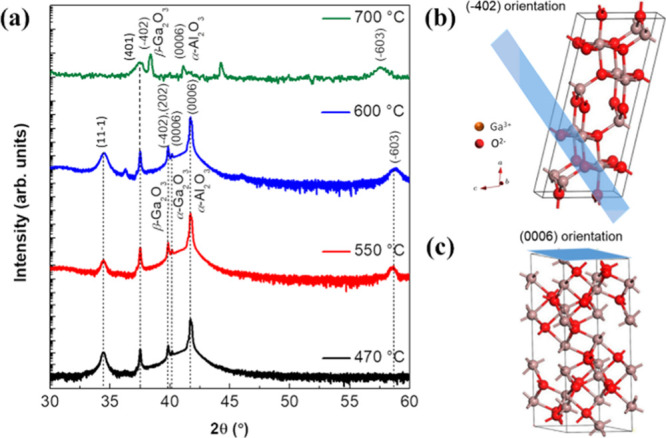
(a) XRD spectra of the Ga2O3 film grown on an α-Al2O3 substrate at 470–700 °C. Unit cell of the (b) β-Ga2O3 (−402) orientation and (c) α-Ga2O3 (0006) orientation.
Table 1. Calculation of Dislocation Density of the Ga2O3 Thin Films at Different Growth Temperatures.
| deposition temp (°C) | peak position, 2θ (deg) | fwhm, β (deg) | cystalline size,D (nm) D = Kλ/β cos θ | dislocation density 10–4 × (nm–2) δ = 1/D2 | average dislocation density (1010cm–2) |
|---|---|---|---|---|---|
| 470 | 37.51822 | 0.0977 | 89.69150821 | 1.24307504 | 2.82 |
| 39.85853 | 0.12962 | 68.09069604 | 2.156872398 | ||
| 40.72352 | 0.19953 | 44.50201341 | 5.049410508 | ||
| 500 | 37.51952 | 0.09831 | 89.1353282 | 1.258636332 | 2.70 |
| 39.85963 | 0.13027 | 67.751184 | 2.178543427 | ||
| 40.72707 | 0.19174 | 46.31058504 | 4.662721381 | ||
| 600 | 37.51688 | 0.09572 | 91.54644328 | 1.19321045 | 2.63 |
| 39.85514 | 0.12691 | 69.54393947 | 2.067670934 | ||
| 40.72305 | 0.19073 | 46.40264667 | 4.644238301 |
Table 2. Deposition Conditions of the Ga2O3 Thin Films.
| phase | precursor concentration (M) | Ar and O2 flow rate (sccm) | deposition temp (°C) and time (h) | average dislocation density (1010× cm–2) | rms (nm) |
|---|---|---|---|---|---|
| α and β | 0.01 | 350 & 50 | 470 & 1 | 2.82 | 16.49 |
| α and β | 0.01 | 350 & 50 | 550 & 1 | 2.70 | 14.79 |
| α and β | 0.01 | 350 & 50 | 600 & 1 | 2.63 | 2.40 |
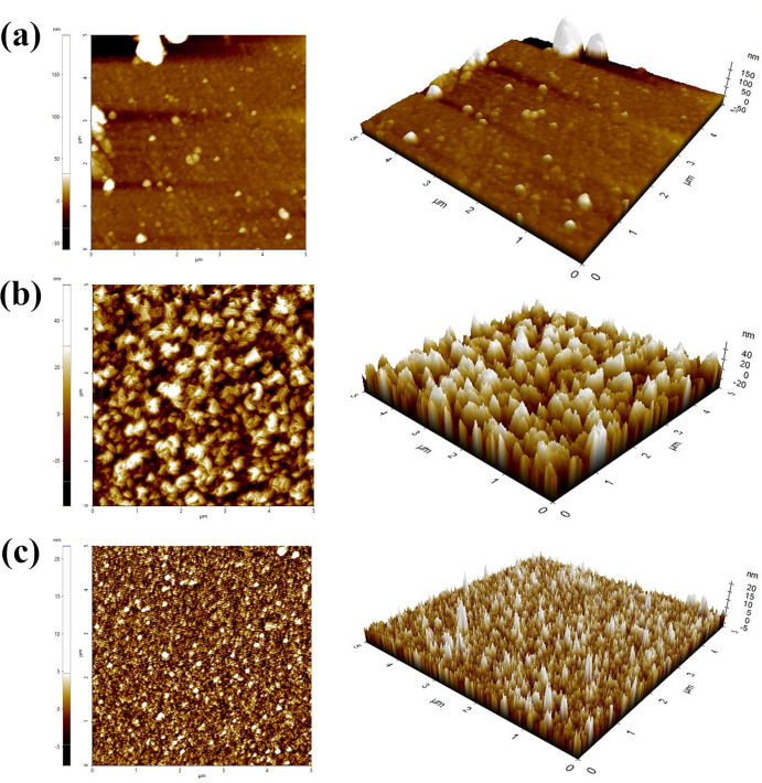
As shown in Figure 2a–c, Ga2O3 thin-film surface roughness and morphology were characterized by AFM with the contact operation mode. 470, 550, and 600 °C grown thin film root-mean-square (rms) surface roughness values of 16.49, 14.79, and 2.40 nm, respectively, were analyzed within an area of 5 × 5 μm2. The rms value represents the standard deviation of the surface height profile over the area.37 It can be seen that the thin-film dislocation density reflects on the surface roughness. This dislocation density has a relation with the crystalline/grain size, which can be found out in XRD analysis. Many grains are present in the different orientations of crystallographic axes. It is shown that 600 °C grown thin films exhibit relatively lower (rms) average surface roughness in comparison of lower growth temperatures, and the surface roughness is uniform in the entire area (Figure 2c). As a result, temperature could play a significant role in the stabilized crystal phase. So far, gaining the higher thermal energy of thin films, β-phase crystallinity reconstruction enables ad-atoms mobility and interface strain slightly less between two crystal materials. The surface nature appears to be consisting of several nuclei growing independently and randomly distributed three-dimensional crystal particles with uniform height. The morphology of the film became more uniform by reducing its surface roughness and increasing its density. The larger lattice mismatch and residual strain caused misfit dislocation to appear on the thin-film surface. It was shown that the sample grown at 600 °C has better surface morphology than the other samples. Therefore, further characterization and analysis were conducted for the sample grown at 600 °C only.
Figure 2.
AFM surface topography characteristics of the Ga2O3 film grown at (a) 470, (b) 550, and (c) 600 °C.
The optical transmittance spectra (250–800 nm) of Ga2O3 samples at 600 °C deposition temperatures were performed using a double-beam spectrometer with a reference α-Al2O3 substrate (Figure 3). Due to the light diffraction, wave curves occur in the UV–visible range. This Ga2O3 sample showed high transmission of about 95% in the UV–visible regions, and their transmissibility began to increase significantly from UV to the visible area. The α- and β-phase Ga2O3 behave as direct band gap semiconductors, and the Tauc equation can determine the Ga2O3 band gap. Figure 3b shows the Tauc equation where the absorption coefficient α is directly proportional to the optical band gap, Eg.
| 3 |
where n = 2 (direct allowed transition) and n = 1/2 (indirect allowed transition), A is the substant-dependent constant, and hυ is the photon energy.33,38 The Eg can be determined by extrapolating the linear region of Tauc’s plot. A is the slope of the linear absorption edge associated with the structural disorder of the Ga2O3. The calculated direct band gap was 5.2 eV for the corresponding grown temperature at 600 °C. This optical band gap lies between 4.9 and 5.1 eV, as described by Kumar et al.39 Also, these band gap characteristics show a redshift absorption edge in this deposition temperature.
Figure 3.
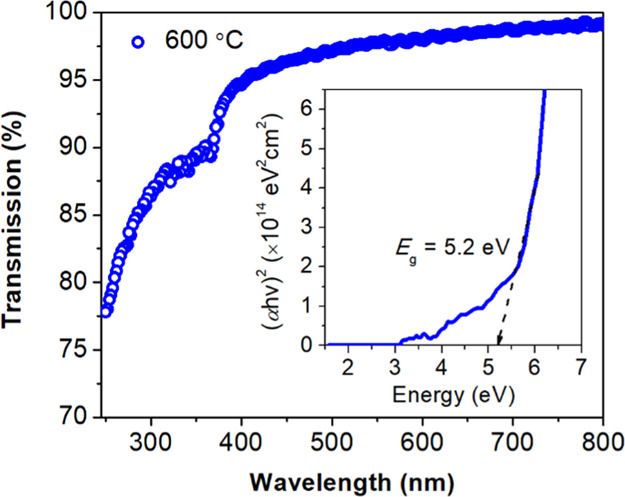
UV–visible optical transmittance spectrum (250–800 nm) of the Ga2O3 thin films grown at 600 °C. The insets show Tauc plots of (αhν)2 as a function of photon energy (E).
Figure 4 shows the measured Raman spectrum of Ga2O3 thin films grown at 600 °C, taken in the range of wavenumber 300–800 cm–1. This Raman spectroscopy tool used a powerful 532 nm excitation source and yielded a 1 μm spot size. In the Raman shift, 419 and 750 cm–1 peaks indicate the sapphire peaks.40 The Raman peak, 451 cm–1, belongs to the C32h space group β-Ga2O3, representing the β-phase bending of GaO4 tetrahedral.41 The lower Raman peak at 431 cm–1 belongs to α-Ga2O3, which is attributed to the Raman allowed vibrational modes Eg. This mode is attributed to Ga atoms vibrating against each other along the c-axis. Another peak A1g mode at 577 cm–1 is due to the lighter oxygen atom vibrations perpendicular to the c-axis.42,43 These obtained Raman modes agree with the experimental and theoretical values reported in the literature.42,43 The low intensity of Raman modes of α-Ga2O3 may be due to little amount of the α phase content in this sample.
Figure 4.
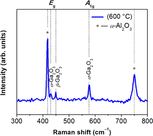
Raman spectrum of the mixed-phase Ga2O3 thin films grown at 600 °C.
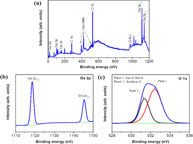
XPS measurements were performed to characterize the surface elemental chemical state of the epilayer. The XPS survey scan exhibited Al, Ga, and O element of the Ga2O3 thin film grown on the α-Al2O3 substrate, as shown in Figure 5a. Figure 5b presents the Ga 2p spectrum that can be split into two main peaks such as Ga 2p3/2 and Ga 2p1/2, having binding energy appearing at 1115.79 and 1142.62 eV. The spin split between these two peaks is approximately 27 eV, consistent with the literature.44 Meanwhile, the binding energy of the Ga 3d peak is 21 eV, which is in good agreement with the literature.45Figure 5c shows that the O 1s can be deconvoluted into two peaks using the Gaussian fitting method. The two peaks located at about 528.1 and 529.2 eV correspond to the Ga–O bond (peak I) and the oxygen-related vacancies (peak II), respectively.46 The hybridization state of surface chemical compositions from the Ga 3d, O 1s, and C 1s peaks was estimated based on the respective sensitivity factors.47 This is consistent with the results of recent findings on the relationship between oxidation and crystal structures.
Figure 5.
(a) XPS survey scan of the as-grown Ga2O3 thin films at 600 °C. (b) Ga 2p and (c) O 1s peaks.
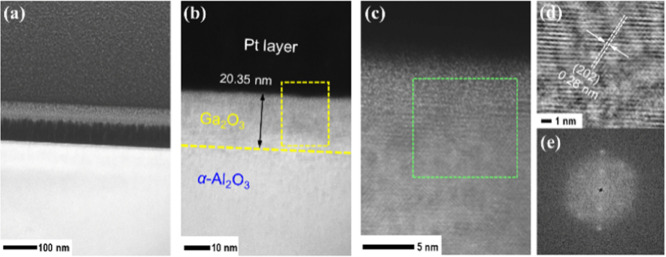
The cross-sectional TEM images revealed the thin-film thickness and interfacial structure of the thin heteroepitaxial mixed-phase Ga2O3. Figure 6a–c shows the cross-sectional TEM images of the as-grown Ga2O3 thin films on the α-Al2O3 substrate at 600 °C, from which 20.35 nm thick Ga2O3 thin films were obtained with a growth rate of 0.339 nm/min. The Ga2O3 microstructure formed an amorphous and crystalline region, and the Ga2O3/Al2O3 interface is not obvious, resulting in high dislocation in-between layers. These misfit dislocations are caused by the interfacial strain formed in the lattice mismatch, as observed by Ma et al.31 The FFT measured interplanar d spacing value is 0.28 nm, corresponding to the (−202) plane of single-crystalline β-Ga2O3 (see Figure 6d), which is identical to the XRD pattern. Figure 6e shows the fast Fourier transform (FFT) pattern of Ga2O3/Al2O3. This Ga2O3 layer is not so obvious and uniform due to the presence of dislocations. The FFT pattern shows the rectangular diffraction patterns in the dark field virtual image. Nevertheless, these diffraction spots are so clear with periodic order of uniform distance. The α-Al2O3 diffraction spots are beneath Ga2O3.
Figure 6.
(a) Cross-sectional TEM of the as-grown Ga2O3 thin films on α-Al2O3 at 600 °C. (b) Cross-sectional high-resolution TEM image showing 20.35 nm thick Ga2O3 films. (c) Close-up view of the Ga2O3 thin films in the yellow dashed line box in (b). (d) Filtered HR-TEM image in the green dashed line box in (c). (e) FFT pattern of Ga2O3/α-Al2O3.
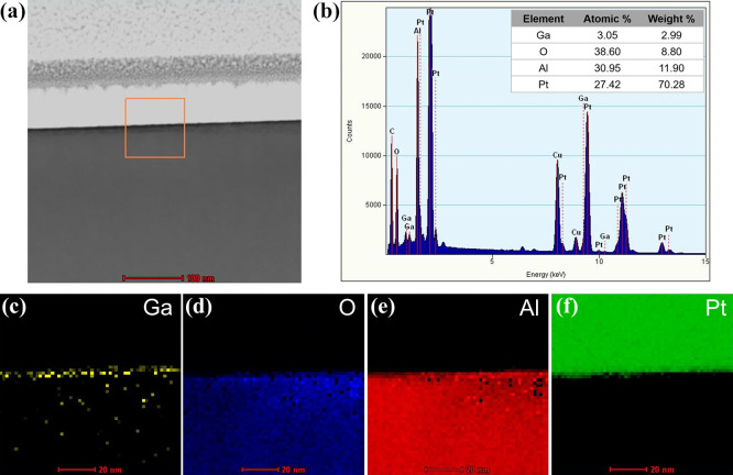
Figure 7 shows cross-sectional analysis of elemental mapping of the Ga2O3 thin films obtained using the energy-dispersive X-ray spectroscopy (EDX) system from the orange box, as shown in Figure 7a. The EDX results provide the elemental composition and mapping for each Ga, O, Al, and Pt, as shown in Figure 7b–f. Here, the results revealed that the Ga has a low concentration at about 3.05 atomic %. It is interesting to note that EDX analysis provides the bulk concentration of elements present in the sample. The high O concentration at 36.60 atomic % may represent both Ga2O3 thin films and α-Al2O3 substrates. Hence, the values of O concentration are inaccurate and not comparable to that of Ga concentration. From the EDX analysis (distribution of O and Ga) here, we can confirm the presence of Ga2O3 thin films grown on the α-Al2O3 substrate.
Figure 7.
TEM–EDX measurements of the as-grown Ga2O3 thin films on α-Al2O3 at 600 °C. (a) Cross-sectional TEM image of the Ga2O3 thin films on the α-Al2O3 substrate. (b) Integrated EDX spectrum of the sample scanned in the orange box in (a). The inset shows the elemental composition in atomic and weight percentage. (e–f) EDX mapping for Ga, O, Al, and Pt element, respectively.
3. Conclusions
The low-cost mist-CVD method has been employed to grow the mixed-phase Ga2O3 thin films on the α-Al2O3 substrate at deposition temperatures of 470–600 °C. Above 600 °C temperature, only a pure β-phase formed on Ga2O3 thin films on the α-Al2O3 substrate. It was found that the Ga2O3 thin films grown at 600 °C have high dislocation density associated with smooth surface roughness. The UV–vis characterization shows that the excellent transmission nature with an optical band gap of 5.2 eV and an ultrathin film of 20.23 nm at 600 °C may be due to the lower precursor concentration with the lower oxygen flow rate. These mixed-phase Ga2O3 thin films would help lead to new promising properties for transistors and deep UV photodetectors.
4. Experimental Studies
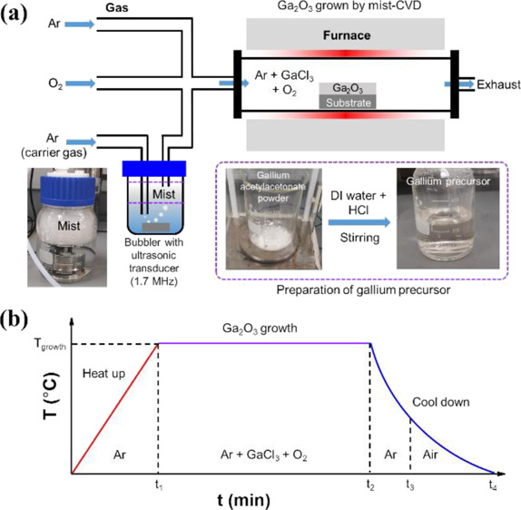
In our work, Ga2O3 thin films were grown on the α-Al2O3 substrates via the low-cost mist-CVD method. As shown in Figure 8a, the mist-CVD method utilizes three main components: mist formation, gas supply and reaction furnace. Table 1 shows that the Ga2O3 thin films were grown on the α-Al2O3 substrate by varying the growth temperature with the minimal oxygen flow rate. A gallium precursor was prepared by dissolving 0.01 mol of gallium acetylacetonate (0.367 gm) into 100 mL of distilled water (DI). Then, a small amount of 1 ml HCl was dropped into the solution to have better dissolution of gallium acetylacetonate during the stirring process. The gallium precursor was atomized by a 1.7 MHz piezoelectric ultrasonication transducer to produce mist in the bubbler unit. The schematic diagram of the overall growth process is shown in Figure 8b. Before growing the Ga2O3 thin films, the α-Al2O3 substrates were cleaned by rinsing with ethanol, acetone, and DI water for 10 min each at room temperature. Then, α-Al2O3 substrates were placed manually in the quartz tube and heated up to the desired growth temperature (470, 550, 600, and 700 °C) in an Argon (Ar) atmosphere for 40 min (t1). After the furnace reached the desired growth temperature, the Ga-containing mist that was kept in a bubbler was transported into the reaction furnace with a 350 sccm Ar flow as carrier gas while another 50 sccm oxygen (O2) flow was transported separately. The O2 gas was used to compensate oxygen vacancies for enhancing the crystallinity of Ga2O3. The typical growth time was about 60 min (t2) at ambient pressure. After completion of the growth, the as-grown Ga2O3 samples were cooled to room temperature in an Ar atmosphere for the first 20 min and in air afterward.
Figure 8.
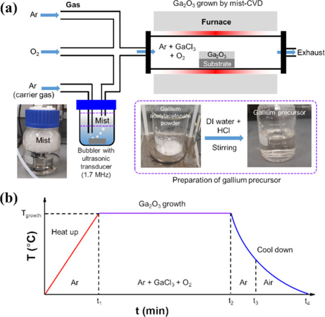
(a) Schematic representations of the mist-CVD system to grow mixed-phase Ga2O3 thin films on the α-Al2O3 substrate. (b) Schematic diagram of the growth temperature as a function of time for the growth of Ga2O3.
Structural crystallinity information of Ga2O3 thin films was analyzed by thin-film high-resolution XRD (SmartLab, Rigaku, Japan) with an X-ray source Cu Kα1 (λ = 1.54056 Å). The thin-film surface roughness profile measurement was performed using Park systems’ AFM. The optical transmission spectra of the samples were characterized using a dual-beam LAMBDA 950 PerkinElmer UV Vis-spectrometer. Raman spectroscopy was carried out using the Thermo Scientific Model: DXR2xi system with 532 nm solid-state laser diode excitation. XPS (Axis Ultra DLD) with monochromatic Al Kα (1486.6 eV) characterized binding energy, and surface elemental analysis was used. Thin-film cross-sectional thickness and elemental percentage were studied by transmission electron microscopy (HR-TEM) of Talos L120C.
Acknowledgments
This work is supported in part by the Universiti Kebangsaan Malaysia (grant no. DIP-2019-018).
The authors declare no competing financial interest.
References
- Hao Y. Gallium oxide: Promise to provide more efficient life. J. Semiconduct. 2019, 40, 010301. 10.1088/1674-4926/40/1/010301. [DOI] [Google Scholar]
- Bayraktaroglu B.Assessment of gallium oxide technology. Air Force Res. Lab. Sensors Dir. WPAFB. The United States No. AFRL-R, 2017, 1–103.
- Ping L. K.; Berhanuddin D. D.; Mondal A. K.; Menon P. S.; Mohamed M. A. Properties and perspectives of ultrawide bandgap Ga2O3 in optoelectronic applications. Chin. J. Phys. 2021, 73, 195–212. 10.1016/j.cjph.2021.06.015. [DOI] [Google Scholar]
- Onuma T.; Saito S.; Sasaki K.; Masui T.; Yamaguchi T.; Honda T.; Higashiwaki M. Valence band ordering in β-Ga2O3 was studied by polarized transmittance and reflectance spectroscopy. Jpn. J. Appl. Phys. 2015, 54, 112601. 10.7567/jjap.54.112601. [DOI] [Google Scholar]
- Kean Ping L.; Mohamed M. A.; Kumar Mondal A.; Mohamad Taib M. F.; Samat M. H.; Berhanuddin D. D.; Menon P. S.; Bahru R. First-Principles Studies for Electronic Structure and Optical Properties of Strontium Doped β-Ga2O3. Micromachine 2021, 12, 348. 10.3390/mi12040348. [DOI] [PMC free article] [PubMed] [Google Scholar]
- Segura A.; Artús L.; Cuscó R.; Goldhahn R.; Feneberg M. Band gap of corundumlike α-Ga2O3 determined by absorption and ellipsometry. Phys. Rev. Mater. 2017, 2, 024604. 10.1103/physrevmaterials.1.024604. [DOI] [Google Scholar]
- Mondal A. K.; Mohamed M. A.; Ping L. K.; Mohamad Taib M. F.; Samat M. H.; Haniff M. A. S. M.; Bahru R. First-principles studies for electronic structure and optical properties of p-type calcium doped α-Ga2O3. Materials 2021, 14, 604. 10.3390/ma14030604. [DOI] [PMC free article] [PubMed] [Google Scholar]
- Kaneko K.; Oda M.; Hitora T.; Fujita S.. Corundum structure Ga2O3 -based alloys for future power device applications. ICEP Proceedings, 2017; pp 156–157.
- Tetelbaum D.; Nikolskaya A. A.; Korolev D. S.; Belov A. I.; Trushin V. N.; Dudin Y. A.; Mikhaylov A. N.; Pechnikov A. I.; Scheglov M. P.; Nikolaev V. I.; Gogova D. Ion-Beam Modification of Metastable Gallium Oxide Polymorphs. Mater. Lett. 2011, 302, 130346. 10.1016/j.matlet.2021.130346. [DOI] [Google Scholar]
- Oshimi H.; Shinohe T.; Majima C.; Nishiguchi Y.; Kurokawa N.; Yamaguchi S.; Nishida K.; Tsuji H.; Mori T.. Development and Manufacture of Devices Using Next-Generation Semiconductor Materials “Gallium Oxide” (GaO Devices), 2011.
- Lee S.-D.; Akaiwa K.; Fujita S. Thermal stability of single-crystalline alpha gallium oxide films on sapphire substrates. Phys. Status Solidi C 2013, 10, 1592–1595. 10.1002/pssc.201300259. [DOI] [Google Scholar]
- Orita M.; Hiramatsu H.; Ohta H.; Hirano M.; Hosono H. Preparation of highly conductive, deep ultraviolet transparent β-Ga2O3 thin film at low deposition temperatures. Thin Solid Films 2002, 411, 134–139. 10.1016/s0040-6090(02)00202-x. [DOI] [Google Scholar]
- Schewski R.; Wagner G.; Baldini M.; Gogova D.; Galazka Z.; Schulz T.; Remmele T.; Markurt T.; Von Wenckstern H.; Grundmann M.; Bierwagen O.; Vogt P.; Albrecht M. Epitaxial stabilization of pseudomorphic α-Ga2O3 on sapphire (0001). Appl. Phys. Exp. 2014, 8, 011101. 10.7567/apex.8.011101. [DOI] [Google Scholar]
- Lu Y. M.; Li C.; Chen X. H.; Han S.; Cao P. J.; Jia F.; Zeng Y. X.; Liu X. K.; Xu W. Y.; Liu W. J.; Zhu D. L. Preparation of Ga2O3 thin film solar-blind photodetectors based on mixed-phase structure by pulsed laser deposition. Chin. Phys. 2019, 28, 018504. 10.1088/1674-1056/28/1/018504. [DOI] [Google Scholar]
- Víllora E. G.; Shimamura K.; Kitamura K.; Aoki K. Rf-plasma-assisted molecular-beam epitaxy of β-Ga2O3. Appl. Phys. Lett. 2006, 88, 031105. 10.1063/1.2164407. [DOI] [Google Scholar]
- Singh Pratiyush A.; Krishnamoorthy S.; Vishnu Solanke S.; Xia Z.; Muralidharan R.; Rajan S.; Nath D. N. High responsivity in molecular beam epitaxy grown β-Ga2O3 metal semiconductor metal solar-blind deep-UV photodetector. Appl. Phys. Lett. 2017, 110, 221107. 10.1063/1.4984904. [DOI] [Google Scholar]
- Okumura H.; Kita M.; Sasaki K.; Kuramata A.; Higashiwaki M.; Speck J. S. Systematic investigation of the growth rate of β-Ga2O3(010) by plasma-assisted molecular beam epitaxy. Appl. Phys. Exp. 2014, 7, 095501. 10.7567/apex.7.095501. [DOI] [Google Scholar]
- Shan F. K.; Liu G. X.; Lee W. J.; Lee G. H.; Kim I. S.; Shin B. C. Structural, electrical, and optical properties of transparent gallium oxide thin films grown by plasma-enhanced atomic layer deposition. J. Appl. Phys. 2005, 98, 023504. 10.1063/1.1980535. [DOI] [Google Scholar]
- Lv Y.; Mi W.; Luan C. N.; Ma J. Structural and optical properties of α-Ga2O3 films deposited on sapphire (1010) and (0112) substrate by MOCVD. Adv. Mater. Res. 2013, 746, 369–373. 10.4028/www.scientific.net/amr.746.369. [DOI] [Google Scholar]
- Kim H. W.; Kim N. H. Growth of gallium oxide thin films on silicon by the metal-organic chemical vapor deposition method. Mater. Sci. Eng., B 2004, 110, 34–37. 10.1016/j.mseb.2004.01.012. [DOI] [Google Scholar]
- Gogova D.; Wagner G.; Baldini M.; Schmidbauer M.; Irmscher K.; Schewski R.; Galazka Z.; Albrecht M.; Fornari R. Structural properties of Si-doped β-Ga2O3 layers grown by MOVPE. J. Cryst. Growth 2014, 401, 665–669. 10.1016/j.jcrysgro.2013.11.056. [DOI] [Google Scholar]
- Gottschalch V.; Mergenthaler K.; Wagner G.; Bauer J.; Paetzelt H.; Sturm C.; Teschner U. Growth of β-Ga2O3 on Al2O3 and GaAs using metal-organic vapor-phase epitaxy. Phys. Status Solidi A 2009, 206, 243–249. 10.1002/pssa.200824436. [DOI] [Google Scholar]
- Gogova D.; Schmidbauer M.; Kwasniewski A. Homo- and heteroepitaxial growth of Sn-doped β-Ga2O3 layers by MOVPE. CrystEngComm 2015, 17, 6744–6752. 10.1039/c5ce01106j. [DOI] [Google Scholar]
- Rafique S.; Han L.; Zhao H. Synthesis of wide bandgap Ga2O3 (Eg ∼ 4.6-4.7 eV) thin films on sapphire by low-pressure chemical vapor deposition. Phys. Status Solidi A 2016, 213, 1002–1009. 10.1002/pssa.201532711. [DOI] [Google Scholar]
- Shinohara D.; Fujita S. Heteroepitaxy of corundum-structured α-Ga2O3 thin films on α-Al2O3 substrates by ultrasonic mist chemical vapor deposition. Jpn. J. Appl. Phys. 2008, 47, 7311–7313. 10.1143/jjap.47.7311. [DOI] [Google Scholar]
- Oshima Y.; Víllora E. G.; Shimamura K. Halide vapor phase epitaxy of twin-free α-Ga2O3 on sapphire (0001) substrates. Appl. Phys. Express 2015, 8, 055501. 10.7567/apex.8.055501. [DOI] [Google Scholar]
- Cheng Y.; Xu Y.; Li Z.; Zhang J.; Chen D.; Feng Q.; Xu S.; Zhou H.; Zhang J.; Hao Y.; Zhang C. Heteroepitaxial growth of α-Ga2O3 thin films on a-, c- and r-plane sapphire substrates by low-cost mist-CVD method. J. Alloys Compd. 2020, 831, 154776. 10.1016/j.jallcom.2020.154776. [DOI] [Google Scholar]
- Kaneko K.; Kawanowa H.; Ito H.; Fujita S. Evaluation of misfit relaxation in α-Ga2O3 epitaxial growth on α-Al2O3. Jpn. J. Appl. Phys. 2012, 51, 020201. 10.1143/jjap.51.020201. [DOI] [Google Scholar]
- Kawaharamura T.; Dang G. T.; Furuta M. Successful growth of conductive highly crystalline Sn-doped α-Ga2O3 thin films by fine-channel mist chemical vapor deposition. Jpn. J. Appl. Phys. 2012, 51, 040207. 10.1143/jjap.51.040207. [DOI] [Google Scholar]
- Lee S.-D.; Kaneko K.; Fujita S. Homoepitaxial growth of beta gallium oxide films by mist chemical vapor deposition. Jpn. J. Appl. Phys. 2016, 55, 1202B8. 10.7567/JJAP.55.1202B8. [DOI] [Google Scholar]
- Ma T. C.; Chen X. H.; Kuang Y.; Li L.; Li J.; Kremer F.; Ren F.-F.; Gu S. L.; Zhang R.; Zheng Y. D.; Tan H. H.; Jagadish C.; Ye J. D. On the origin of dislocation generation and annihilation in α-Ga2O3 epilayers on sapphire. Appl. Phys. Lett. 2019, 115, 182101. 10.1063/1.5120554. [DOI] [Google Scholar]
- Son H.; Choi Y. J.; Hwang J.; Jeon D. W. Influence of post-annealing on properties of α-Ga2O3 epilayer grown by halide vapor phase epitaxy. ECS J. Solid State Sci. Technol. 2019, 8, Q3024–Q3027. 10.1149/2.0051907jss. [DOI] [Google Scholar]
- Li J.; Chen T.; Cui X.; Ren F.-F.; Gu S.; Zhang R.; Zheng Y.; Ringer S. P.; Fu L.; Tan H. H.; Jagadish C.; Ye J. Identification and modulation of electronic band structures of single-phase β-(AlxGa1-x)2O3 alloys grown by laser molecular beam epitaxy. Appl. Phys. Lett. 2018, 113, 041901. 10.1063/1.5027763. [DOI] [Google Scholar]
- Marezio M.; Remeika J. P. Bond lengths in the α-Ga2O3 structure and the high-pressure phase of Ga2-xFexO3. J. Chem. Phys. 1967, 46, 1862–1865. 10.1063/1.1840945. [DOI] [Google Scholar]
- Williamson G. K.; Smallman R. E. Dislocation densities in some annealed and cold-worked metals from measurements on the X-ray Debye-Scherrer spectrum. Philos. Mag. 1956, 1, 34–46. 10.1080/14786435608238074. [DOI] [Google Scholar]
- Patterson A. L. The Scherrer formula for X-ray particle size determination. Phys. Rev. 1939, 56, 978–982. 10.1103/physrev.56.978. [DOI] [Google Scholar]
- Bhushan B.Surface roughness analysis and measurement techniques. Modern Tribology Handbook, Two Volume Set, Mechanics & Materials Science; CRC Press, 2000, pp 79–150. [Google Scholar]
- Guo D.; Wu Z.; Li P.; An Y.; Liu H.; Guo X.; Yan H.; Wang G.; Sun C.; Li L.; Tang W. Fabrication of β-Ga2O3 thin films and solar-blind photodetectors by laser MBE technology. Opt. Mater. Express. 2014, 4, 1067–1076. 10.1364/ome.4.001067. [DOI] [Google Scholar]
- Kumar S. S.; Rubio E.J.; Noor-A-Alam M.; Martinez G.; Manandhar S.; Shutthanandan V.; Thevuthasan S.; Ramana C.V. Structure, Morphology, and Optical Properties of Amorphous and Nanocrystalline Gallium oxide thin films. J. Phys. Chem. C 2013, 117, 4194. 10.1021/jp311300e. [DOI] [Google Scholar]
- Kiefer W. Recent Advances in linear and nonlinear Raman spectroscopy I. J. Raman Spectrosc. 2007, 38, 1538–1553. 10.1002/jrs.1902. [DOI] [Google Scholar]
- Phumying S.; Labauyai S.; Chareonboon W.; Phokha S.; Maensiri S. Optical properties of β-Ga2O3 nanorods synthesized by a simple and cost-effective method using egg white solution. Jpn. J. Appl. Phys. 2015, 54, 06FJ13. 10.7567/jjap.54.06fj13. [DOI] [Google Scholar]
- Cuscó R.; Domènech-Amador N.; Hatakeyama T.; Yamaguchi T.; Honda T.; Artús L. Lattice dynamics of a mist-chemical vapor deposition-grown corundum-like Ga2O3 single crystal. J. Appl. Phys. 2015, 117, 185706. 10.1063/1.4921060. [DOI] [Google Scholar]
- Xu Y.; Zhang C.; Cheng Y.; Li Z.; Cheng Y. N.; Feng Q.; Chen D.; Zhang J.; Hao Y. Influence of carrier gases on the quality of epitaxial corundum-structured α-Ga2O3 films grown by mist chemical vapor deposition method. Materials 2019, 12, 3670. 10.3390/ma12223670. [DOI] [PMC free article] [PubMed] [Google Scholar]
- Kong L.; Ma J.; Luan C.; Mi W.; Lv Y. Structural and optical properties of heteroepitaxial beta Ga 2O3 films grown on MgO (100) substrates. Thin Solid Films 2012, 520, 4270–4274. 10.1016/j.tsf.2012.02.027. [DOI] [Google Scholar]
- Dong L.; Jia R.; Xin B.; Zhang Y. Effects of post-annealing temperature and oxygen concentration during sputtering on the structural and optical properties of β-Ga 2O3 films. J. Vac. Sci. Technol., A 2016, 34, 060602. 10.1116/1.4963376. [DOI] [Google Scholar]
- Thomas S. R.; Adamopoulos G.; Lin Y.-H.; Faber H.; Sygellou L.; Stratakis E.; Pliatsikas N.; Patsalas P. A.; Anthopoulos T. D. High electron mobility thin-film transistors based on Ga2O3 grown by atmospheric ultrasonic spray pyrolysis at low temperature. Appl. Phys. Lett. 2014, 105, 092105. 10.1063/1.4894643. [DOI] [Google Scholar]
- Ramana C. V.; Rubio E. J.; Barraza C. D.; Miranda G. A.; McPeak S.; Kotru S.; Grant J. T. Chemical bonding, optical constants, and electrical resistivity of sputter-deposited gallium oxide thin films. J. Appl. Phys. 2014, 115, 043508. 10.1063/1.4862186. [DOI] [Google Scholar]


