Abstract
In this study, we investigate a physical mechanism to improve the light absorption efficiency of graphene monolayer from the universal value of 2.3% to about 30% in the visible and near-infrared wavelength range. The physical mechanism is based on the diffraction coupling of surface plasmon polariton resonances in the periodic array of metal nanoparticles. Through the physical mechanism, the electric fields on the surface of graphene monolayer are considerably enhanced. Therefore, the light absorption efficiency of graphene monolayer is greatly improved. To further confirm the physical mechanism, we use an interaction model of double oscillators to explain the positions of the absorption peaks for different array periods. Furthermore, we discuss in detail the emerging conditions of the diffraction coupling of surface plasmon polariton resonances. The results will be beneficial for the design of graphene-based photoelectric devices.
Keywords: graphene monolayer, absorption efficiency, diffraction coupling, plasmon resonance
1. Introduction
When the visible and near-infrared electromagnetic waves are normally incident on the surface of an undoped graphene monolayer suspended in the air, only several percentage points of electromagnetic waves are absorbed by the graphene monolayer. The absorption efficiency (A) of graphene monolayer can be estimated by its fine structure constant (α), which is, A = πα = πe2/ℏc ≈ 2.3%. Here, c is the light speed, ℏ is the reduced Planck’s constant, e is the electron charge, and π is the circumference ratio. The absorption efficiency of 2.3% is a universal value, which does not depend on the wavelength of electromagnetic waves in near-infrared, visible, and even violet regions [1,2]. Due to the considerably good optical and electrical properties, graphene is known to hold a great promising potential in photoelectric devices, such as photodetectors, modulators, perfect absorbers, photovoltaics, photocatalysts, etc. [3,4,5,6,7,8,9,10,11,12,13,14,15,16,17,18]. However, the absorption efficiency of 2.3% is too low for the efficient operation of graphene-based photoelectric devices. Recently, to overcome the difficulty, a number of different solutions have been proposed [19,20], which mainly include surface plasmon polariton resonances [21,22], magnetic resonances [23,24], guided mode resonances [25,26], total internal reflections [27,28], Fabry-Perot resonances [29,30], surface bound states of photonic crystals [31,32], waveguide modes [33], coherent optical beams [34], etc. The fundamental physical principle of these different solutions is to greatly enhance the electric field intensity on the surface of graphene monolayer, and thus improve the absorption efficiency of graphene. In far-infrared and THz regions, the graphene monolayer itself is able to support surface plasmon polariton resonances, which can be utilized to enhance the absorption in graphene [35,36]. However, in the visible and near-infrared regions, the graphene monolayer no longer has this capability, and the other kinds of plasmon resonances in metal nanostructures can be employed to improve the absorption of graphene [37].
The diffraction coupling phenomenon of surface plasmon polariton resonances in the periodic array of metal nanoparticles was theoretically predicted in the early years [38,39], and then it was observed experimentally [40,41]. This diffraction coupling can produce remarkably narrow collective resonances and came to be known as plasmonic surface lattice resonances [42]. In recent years, plasmonic surface lattice resonances have received increasing interest [43], owing to their extremely narrow linewidth and their accompanied great electromagnetic field enhancement. In this experiment, the metal nanoparticle array is commonly prepared on a dielectric substrate. However, it is hard to observe strong surface lattice resonances due to the mismatch in the refractive index of the dielectric substrate and the air [44]. To solve this problem, metal nanoparticles can be lifted by dielectric pillars [45,46] or covered by a dielectric layer with a similar refractive index as the dielectric substrate [47,48]. At present, plasmonic surface lattice resonances are able to provide a large amount of potential applications, such as refractive index sensing [45,46], fluorescent emission [47,48], and tunable lasing [49,50]. To date, there is no report regarding the application of plasmonic surface lattice resonances in improving the light absorption of graphene monolayer.
In this work, we study how to use plasmonic surface lattice resonances to improve the light absorption efficiency of graphene monolayer in the visible and near-infrared wavelength range. The surface lattice resonances result from the collective diffraction coupling effect of localized surface plasmon polariton resonances in gold nanospheres arranged into a periodic array. Through the excitation of surface lattice resonances, the electric fields on the surface of graphene monolayer are considerably enhanced. Therefore, the light absorption in graphene is greatly improved. To well explain the aforementioned physical mechanism, we also employ an interaction model of double oscillators in order to predict the positions of absorption peaks for different array periods. Furthermore, we discuss the emerging conditions of surface lattice resonances. Therefore, our work will be helpful in designing graphene-based photoelectric devices.
2. Methods
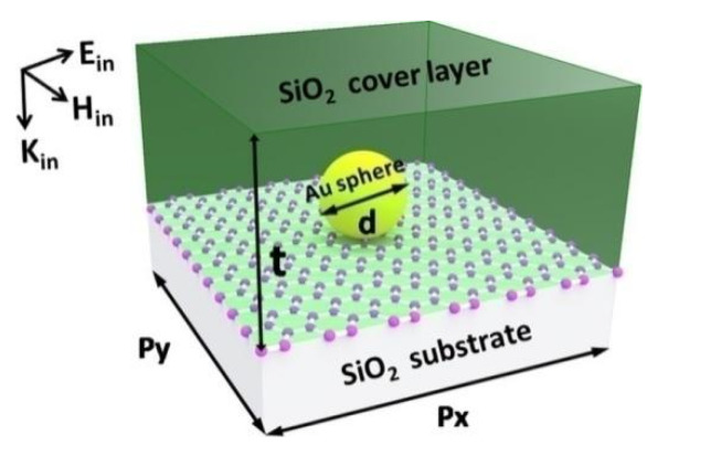
The investigated nanostructure is schematically shown in Figure 1. The graphene monolayer is placed on the dielectric substrate of SiO2. The Au nanospheres on the surface of the graphene monolayer are arranged into periodic arrays, which are covered by the layer of SiO2. In this work, we have used a commercial software package “EastFDTD 5.0” (https://www.eastfdtd.com, accessed on 1 September 2013) to calculate the absorption spectra of the graphene monolayer in the visible and near-infrared regions. In addition, some relevant electromagnetic field distributions are calculated by this commercial software package. In our numerical calculations, the Au nanospheres have a complex refractive index, which is dependent on the wavelength of the incident light. The complex refractive index can be obtained from the experimental data [51]. The diameter d of the Au nanospheres is 150 nm. The array periods of the Au nanospheres are px and py along the x-axis and the y-axis directions, respectively. Each Au nanosphere is able to support the excitation of the localized surface plasmon polariton resonance [52,53,54,55,56]. The SiO2 substrate and the SiO2 cover layer have a constant refractive index of 1.45. The thickness t of the SiO2 cover layer is 500 nm. The most important role played by the SiO2 cover layer is to make the surrounding medium of the Au nanospheres homogeneous, and thus realize the diffraction coupling of the localized surface plasmon polariton resonance. The thickness of the graphene monolayer is 0.34 nm. For different wavelengths, the surface conductivity and the anisotropic relative permittivity of the graphene monolayer can be calculated by analytical expressions [57]. In Figure 1, the light is normally incident from top to bottom. The directions of the electric field Ein, the magnetic field Hin, and the wave vector Kin of the incident light, are indicated by the black arrows in the top left corner. The basic principle of the simulation software is the finite difference time domain method of electromagnetic wave, which is based on the well-known Maxwell equations. In the numerical simulation, we set two perfectly matched layers with a thickness of 500 nm to completely eliminate the reflection of the electromagnetic wave in the positive and negative directions of the z-axis. Considering the periodicity of the structure, we also set two periodic boundary conditions in the two directions of the x-axis and the y-axis, respectively. To achieve reliable results with numerical convergence, the mesh size in the regions of graphene is Δs = 0.05 nm, and the mesh size in the other material regions is Δs = 20 nm. Similarly, the time step is set to be Δt = Δs/2c, where c is the speed of light propagating in a vacuum. As the light source, a Gauss pulse with a center wavelength of 900 nm is normally incident on the studied structure.
Figure 1.
The unit cell of the investigated structure to enhance the light absorption of graphene monolayer.
3. Results and Discussion
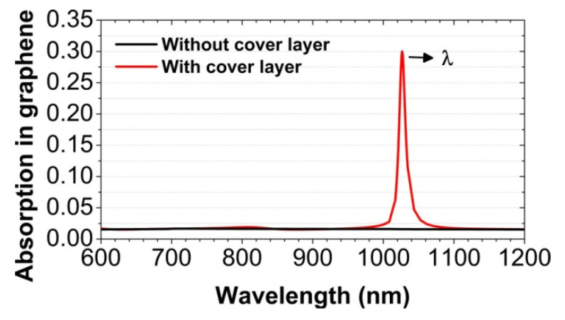
In Figure 2, we show the normal-incidence absorption spectra of the graphene monolayer in the visible and near-infrared wavelength range from 600 to 1200 nm, for the two cases: With or without the cover layer of SiO2. In the case with the cover layer (see the red line), we observe an obvious absorption peak, which is centered at the wavelength of λ = 1026.5 nm. At the peak, the maximum absorption efficiency of the graphene monolayer can reach up to 30%, which is far larger than the universal value of 2.3%. This light absorption enhancement in the graphene monolayer is beneficial to the graphene-based photoelectric devices. The absorption peak is relatively narrow, which has a full width at half maximum (FWHM) of about 10 nm. The physical mechanism of the absorption peak is the collective diffraction coupling effect of the surface plasmon polariton resonance in the periodic array of Au nanospheres. For comparison, we have also calculated the corresponding absorption spectra in the case without the cover layer. As clearly shown by the black line in Figure 2, the absorption peak will disappear. In the case without the cover layer, the Au nanospheres no longer have a homogeneous surrounding medium. The collective diffraction coupling effect will not happen, due to the mismatch in the refractive index of the dielectric substrate and the air [58].
Figure 2.
The numerically calculated absorption spectra of the graphene monolayer at normal incidence. Geometrical parameters: The array periods px = 400 nm and py = 700 nm; the diameter of the Au nanospheres d = 150 nm; the thickness of the SiO2 cover layer t = 500 nm.
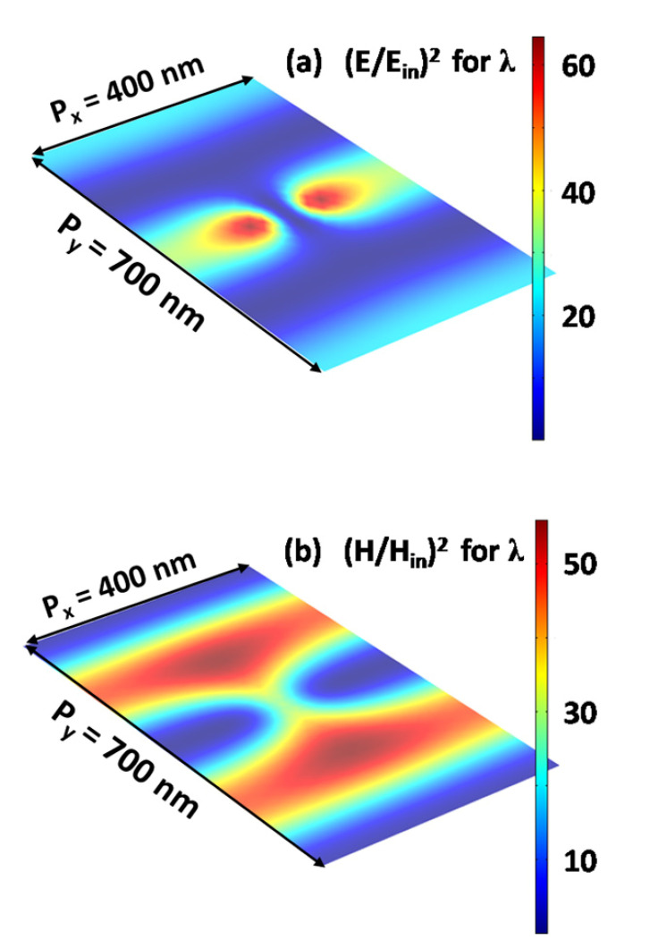
To effectively understand the physical mechanism of the absorption peak, we calculated the electromagnetic field intensities at the wavelength of λ = 1026.5 nm on the xy plane, as shown in Figure 3. Two “hotspots” of electric fields near the Au nanosphere are clearly seen in Figure 3a, which result from the excitation of the localized dipolar plasmon polariton resonance of the Au nanosphere. In addition to the two “hotspots”, there are three parallel belt-shaped regions of the electric field enhancement in Figure 3a, and two parallel belt-shaped regions of the magnetic field enhancement in Figure 3b. These regions of electromagnetic fields are the trails of the diffraction wave propagating along the y-axis direction. In the investigated wavelength range from 600 to 1200 nm, the period px is only 400 nm. Therefore, all of the diffraction channels along the x-axis direction are closed completely. However, the zero-order diffraction channel along the y-axis direction is open for the period py = 700 nm. When the zero-order diffraction wave grazes the array of the Au nanospheres, it will strongly interact with the localized dipolar plasmon polariton resonance. This interaction is able to enhance the electric fields on the surface of the graphene monolayer, and thus improve the light absorption efficiency of graphene.
Figure 3.
The intensity distributions of the electric fields (a) and the magnetic fields (b) on the surface of the graphene monolayer at the wavelength of λ = 1026.5 nm.
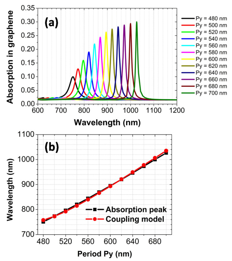
As discussed above, by properly designing the array periods of the Au nanospheres, the diffraction channel along the x-axis direction can be closed, and only the zero-order diffraction channel along the y-axis direction is open. The zero-order diffraction channel appears near the well-known Wood anomaly, whose wavelength depends on the array period py (λWood = npy, n = 1.45 is the refractive index of the SiO2). Therefore, by changing the array period py, we can tune the position of the absorption peak. In Figure 4a, we have calculated the normal-incidence absorption spectra of the graphene monolayer, when the array period py is increased from 480 to 700 nm in steps of 20 nm. When the value of py is increased, it is clearly seen that the absorption peak shifts to the higher wavelength accordingly. To further confirm the physical mechanism of the absorption peak, we have used the interaction model of double oscillators [59] to predict the position of the absorption peak for different array periods py. The black square in Figure 4b gives the practical position of the absorption peak, which is obtained from Figure 4a. The red circle in Figure 4b gives the corresponding position predicted using the interaction model, which is in a good agreement with the practical position. In the interaction model, one oscillator is the localized dipolar plasmon polariton resonance of the Au nanosphere, whose resonance wavelength is 720 nm. The other oscillator is the zero-order diffraction wave along the y-axis direction, whose resonance wavelength is at the Wood anomaly. The interaction strength between these two oscillators is taken as Δ = 25 meV. This value of Δ is chosen to satisfactorily predict the practical position of the absorption peak. The predicted position of the absorption peak is obtained by the following formula:
| (1) |
where EWood and ELSP are the photon energies at the Wood anomaly and the localized dipolar plasmon polariton resonance, respectively. The corresponding wavelength of the photon energy E is the predicted position of the absorption peak.
Figure 4.
(a) The absorption spectra of the graphene monolayer for the different array periods py. (b) The dependence of the absorption peak on the array period py.
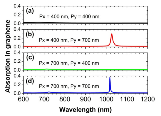
Here, we will discuss the emerging conditions of the diffraction coupling of localized dipolar plasmon polariton resonance in the periodic nanosphere array. To achieve a strong collective effect of diffraction coupling, the surrounding medium of the Au nanospheres should be homogeneous, and the cover layer of SiO2 plays this role, as shown in Figure 1. In addition to this necessary condition, some other conditions should be satisfied, as well. First, the period of the nanosphere array should be large enough for the zero-order diffraction channels to be open in the investigated wavelength range from 600 to 1200 nm. If the period is too small, the collective effect of diffraction coupling will not happen. As clearly seen in Figure 5a, the absorption peak of the graphene monolayer disappears, when the array period py is also shortened to be 400 nm. However, when the array period py is set to be 700 nm, the absorption peak will appear, as shown in Figure 5b. Second, the propagation direction of the diffraction wave must be perpendicular to the polarization direction of the localized dipolar plasmon polariton resonance. In all of the cases studies in this work, the electric field of the incident light is always along the x-axis direction. Therefore, the polarization direction of the localized dipolar plasmon polariton resonance also remains along the x-axis direction. For the array periods of px = 400 nm and py = 700 nm, the diffraction wave propagates along the y-axis direction. In this case, the propagation direction of the diffraction wave and the polarization direction of the localized dipolar plasmon polariton resonance are mutually perpendicular. The above two conditions are satisfied simultaneously. Therefore, we can observe an absorption peak in Figure 5b. In contrast, for the array periods of px = 700 nm and py = 400 nm, the diffraction wave propagates along the x-axis direction, whose propagation direction is parallel to the polarization direction of the localized dipolar plasmon polariton resonance. For this situation, the second condition is not satisfied. Therefore, in Figure 5c, we could not observe an absorption peak. In Figure 5d, with the array periods of px = py = 700 nm, the zero-order diffraction channels along the x-axis direction and the y-axis direction are both open, and the second condition is also satisfied for the diffraction wave propagating along the y-axis direction. As a result, the absorption peak can exist, as well.
Figure 5.
The calculated absorption spectra of the graphene monolayer for different array periods at normal incidence.
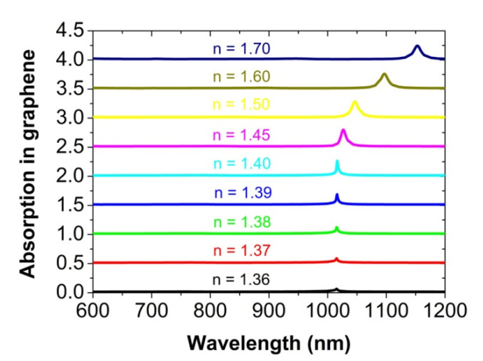
Next, we will consider the influences of some factors on the absorption peak of the graphene monolayer. Figure 6 shows the effect of a refractive index mismatch between the dielectric substrate and the covering medium. When the refractive index n of the covering medium decreases from 1.45 to 1.36, the light absorption efficiency of the graphene monolayer will be reduced quickly from 30% to about 6.5%. For the refractive index n of the covering medium to be increased from 1.45 to 1.70, the absorption of the graphene monolayer will also be reduced slowly to about 24%. The refraction index mismatch results in different phase velocities for the diffractive wave to propagate above and below the substrate [41,42]. If a very large difference in the refractive index is found between the cover layer and the dielectric substrate, it is hard to realize a strong interaction between the diffractive wave and the localized dipolar plasmon polariton resonances of Au nanospheres [44]. As a result, the plasmonic surface lattice resonance mode in the metal nanoparticle arrays could not be formed, and the absorption peak of the graphene monolayer will also disappear. In addition, with the increasing value of the refractive index n, the absorption peak of the graphene monolayer will red-shift, since the wavelength of the Wood anomaly becomes longer. At the same time, the bandwidth of the absorption peak will be broader, due to the larger radiation decay of the plasmonic surface lattice resonance mode.
Figure 6.
The calculated absorption spectra of the graphene monolayer for the different refractive index n of the cover layer at normal incidence. For clarity, the above absorption spectrum is vertically offset by 0.5 from the one below.
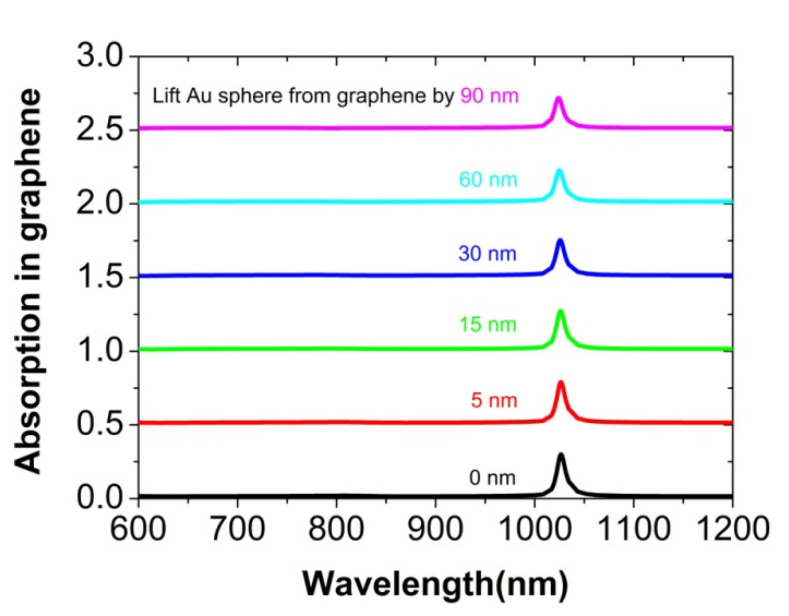
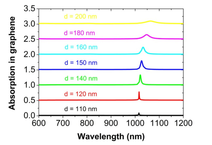
The distance between the graphene and the nanosphere array is another factor to affect the light absorption of the graphene, as shown in Figure 7. When the Au nanosphere is lifted from the graphene monolayer by 5 to 90 nm, the absorption peak will decrease gradually to 22%, since the plasmonic near-field near the graphene becomes weak. Moreover, we have studied the influence of the size of the Au nanosphere on the absorption peak, which is shown in Figure 8. For the diameter d of the Au nanosphere to be about 160 nm, the graphene has a maximum absorption of about 33% at the plasmonic surface lattice resonance. When the diameter d increases to 200 nm, the peak value will be reduced to about 10%. In this case of larger diameter, the Au sphere array reflects more incident light, and thus reduces the absorption in graphene. If the diameter d is only 110 nm, the absorption peak will almost not exist, since the diffraction coupling of surface plasmon polariton resonance among the Au nanospheres is very weak [44]. It is well known that the absorption and the scattering of an individual nanosphere are radius-dependent, which are directly proportional to r3 and r6, respectively, in the long-wave limit, in which the wavelength of the incident light is far larger than the size of a nanosphere [60]. In our work, this radius-dependent relation is not found, since the long-wave limit condition is not well satisfied and simultaneously there is a strong interaction among the Au nanospheres. At the plasmonic surface lattice resonance, the absorption of the Au nanospheres is about 12%, but it is very low for other wavelengths from 600 to 1200 nm.
Figure 7.
The calculated absorption spectra of the graphene monolayer at normal incidence, when the Au nanosphere is lifted from the graphene by different distances. For clarity, the above absorption spectrum is vertically offset by 0.5 from the one below.
Figure 8.
The normal-incidence absorption spectra of the graphene monolayer for the different diameters d of the Au nanosphere. For clarity, the above absorption spectrum is vertically offset by 0.5 from the one below.
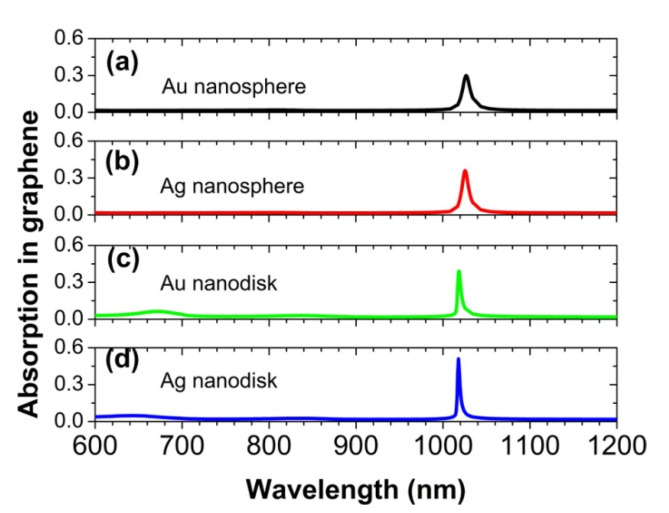
In Figure 9, we have also studied the effects of different metal materials and different nanoparticle shapes on the absorption peak of graphene. When the Au nanosphere is replaced by an Ag nanosphere, the absorption peak becomes a little sharper and increases slightly to 36%, owing to the relatively smaller Joule loss in the Ag material. For the Au nanosphere to be replaced by Au nanodisk or Ag nanodisk, the absorption peak of graphene becomes much narrower, which is able to reach 39% and 51%, respectively. This proves that the proposed physical mechanism is universal. The key role played by the periodical array of metal nanoparticles is to excite the plasmonic surface lattice resonance, which can greatly enhance the electric fields on the surface of graphene, and thus improve the light absorption efficiency of the graphene monolayer. Finally, we should mention that the two oscillator models are still applicable to the above modified parameters. However, the excitation wavelength of the surface plasmon polariton resonance of metal nanoparticles will change for different parameters. Similarly, the interaction strength Δ will also change, which must be reset to accurately predict the position of the absorption peak.
Figure 9.
The normal-incidence absorption spectra of the graphene monolayer, for the Au nanosphere to be replaced by the Ag nanosphere, the Au nanodisk, and the Ag nanodisk, respectively. The array periods are px = 400 nm and py = 700 nm. The nanospheres have a diameter of 150 nm. The nanodisks have a diameter of 120 nm and a thickness of 60 nm.
4. Conclusions
In summary, we have investigated a physical mechanism for enhancing the light absorption efficiency of graphene monolayer from the universal value of 2.3% to about 30% in the visible and near-infrared wavelength range. The physical mechanism is based on the collective diffraction coupling effect of localized surface plasmon polariton resonance in the periodic array of metal nanoparticles. Through this collective diffraction coupling effect, the electric fields on the surface of graphene monolayer are considerably enhanced, and thus the light absorption efficiency of graphene monolayer is greatly improved. To further confirm the physical mechanism, we have used the interaction model of double oscillators to predict the positions of the absorption peaks for different array periods. Moreover, we have discussed in detail the emerging conditions of the collective diffraction coupling effect. First, the array period should be large enough for the zero-order diffraction channels to be open in the investigated wavelength range. Second, the propagation direction of the diffraction wave must be perpendicular to the polarization direction of the localized dipolar plasmon polariton resonance. In addition, for the collective diffraction coupling effect to take place, the surrounding medium of the metal nanoparticle array should be homogeneous. The above results are beneficial for the design of the graphene-based photoelectric devices.
Author Contributions
Conceptualization, investigation, writing—original draft, B.L.; conceptualization, investigation, writing—original draft, W.Y.; conceptualization, investigation, writing—original draft, Z.Y.; investigation, writing—original draft, P.C.; investigation, writing—original draft, F.G.; conceptualization, writing—review and editing, C.T.; investigation, writing—original draft, P.G.; conceptualization, writing—review and editing, Z.L.; conceptualization, investigation, writing—original draft, J.C. All authors have read and agreed to the published version of the manuscript.
Funding
This research was funded by the National Natural Science Foundation of China (NSFC) (11904141, 11974188, 11704183, 11704184, 11804134, 61705197, 12074151, and 11304159), Changzhou Science and Technology Bureau (CJ20190072), Natural Science Foundation of Jiangsu Province (BK20191031 and BK20161512), Natural Science Foundation of Jiangxi Province (2018ACB21005), Natural Science Foundation of Zhejiang Province (LY22A040003, LQ17C100002), China Postdoctoral Science Foundation (2021T140339 and 2018M632345), Jiangsu Postdoctoral Science Foundation (No. 2021K617C), and Qing Lan Project of Jiangsu Province.
Institutional Review Board Statement
Not applicable.
Informed Consent Statement
Not applicable.
Data Availability Statement
The data presented in this study are available on request from the first or corresponding author.
Conflicts of Interest
The authors declare no conflict of interest.
Footnotes
Publisher’s Note: MDPI stays neutral with regard to jurisdictional claims in published maps and institutional affiliations.
References
- 1.Nair R.R., Blake P., Grigorenko A.N., Novoselov K.S., Booth T.J., Stauber T., Peres N.M.R., Geim A.K. Fine Structure Constant Defines Visual Transparency of Graphene. Science. 2008;320:1308. doi: 10.1126/science.1156965. [DOI] [PubMed] [Google Scholar]
- 2.Dawlaty J.M., Shivaraman S., Strait J., George P., Chandrashekhar M., Rana F., Spencer M.G., Veksler D., Chen Y. Measurement of the optical absorption spectra of epitaxial graphene from terahertz to visible. Appl. Phys. Lett. 2008;93:131905. doi: 10.1063/1.2990753. [DOI] [Google Scholar]
- 3.Ferrari A.C., Bonaccorso F., Fal’ko V., Novoselov K.S., Roche S., Bøggild P., Borini S., Koppens F.H.L., Palermo V., Pugno N., et al. Science and technology roadmap for graphene, related two-dimensional crystals, and hybrid systems. Nanoscale. 2015;7:4598–4810. doi: 10.1039/C4NR01600A. [DOI] [PubMed] [Google Scholar]
- 4.Liu C.-H., Chang Y.-C., Norris T.B., Zhong Z. Graphene photodetectors with ultra-broadband and high responsivity at room temperature. Nat. Nanotechnol. 2014;9:273–278. doi: 10.1038/nnano.2014.31. [DOI] [PubMed] [Google Scholar]
- 5.Koppens F., Mueller T., Avouris P., Ferrari A.C., Vitiello M.S., Polini M. Photodetectors based on graphene, other two-dimensional materials and hybrid systems. Nat. Nanotechnol. 2014;9:780–793. doi: 10.1038/nnano.2014.215. [DOI] [PubMed] [Google Scholar]
- 6.Liu Z., Liu Q., Huang Y., Ma Y., Yin S., Zhang X., Sun W., Chen Y. Organic Photovoltaic Devices Based on a Novel Acceptor Material: Graphene. Adv. Mater. 2008;20:3924–3930. doi: 10.1002/adma.200800366. [DOI] [Google Scholar]
- 7.Echtermeyer T., Britnell L., Jasnos P.K., Lombardo A., Gorbachev R., Grigorenko A.N., Geim A.K., Ferrari A.C., Novoselov K. Strong plasmonic enhancement of photovoltage in graphene. Nat. Commun. 2011;2:1–5. doi: 10.1038/ncomms1464. [DOI] [PubMed] [Google Scholar]
- 8.Zhang N., Zhang Y., Xu Y.-J. Recent progress on graphene-based photocatalysts: Current status and future perspectives. Nanoscale. 2012;4:5792–5813. doi: 10.1039/c2nr31480k. [DOI] [PubMed] [Google Scholar]
- 9.Liu Z., Zhou J., Liu X., Fu G., Liu G., Tang C., Chen J. High-Q plasmonic graphene absorbers for electrical switching and optical detection. Carbon. 2020;166:256–264. doi: 10.1016/j.carbon.2020.05.046. [DOI] [Google Scholar]
- 10.Yan Z., Zhu Q., Wan M., Lu X., Pu X., Tang C., Yu L. Graphene ultraviolet ultrahigh-Q perfect absorption for nanoscale optical sensing. Opt. Express. 2020;28:6095–6101. doi: 10.1364/OE.385658. [DOI] [PubMed] [Google Scholar]
- 11.Yan Z., Lu X., Du W., Lv Z., Tang C., Cai P., Gu P., Chen J., Yu Z. Ultraviolet graphene ultranarrow absorption engineered by lattice plasmon resonance. Nanotechnology. 2021;32:465202. doi: 10.1088/1361-6528/ac1af9. [DOI] [PubMed] [Google Scholar]
- 12.Teng D., Wang K., Li Z. Graphene-Coated Nanowire Waveguides and Their Applications. Nanomaterials. 2020;10:229. doi: 10.3390/nano10020229. [DOI] [PMC free article] [PubMed] [Google Scholar]
- 13.Cheng J., Fan F., Chang S. Recent Progress on Graphene-Functionalized Metasurfaces for Tunable Phase and Polarization Control. Nanomaterials. 2019;9:398. doi: 10.3390/nano9030398. [DOI] [PMC free article] [PubMed] [Google Scholar]
- 14.Nurrohman D., Chiu N.-F. A Review of Graphene-Based Surface Plasmon Resonance and Surface-Enhanced Raman Scattering Biosensors: Current Status and Future Prospects. Nanomaterials. 2021;11:216. doi: 10.3390/nano11010216. [DOI] [PMC free article] [PubMed] [Google Scholar]
- 15.Liu C., Guo J., Yu L., Li J., Zhang M., Li H., Shi Y., Dai D. Silicon/2D-material photodetectors: From near-infrared to mid-infrared. Light. Sci. Appl. 2021;10:1–21. doi: 10.1038/s41377-021-00551-4. [DOI] [PMC free article] [PubMed] [Google Scholar]
- 16.Yin J., Liu L., Zang Y., Ying A., Hui W., Jiang S., Zhang C., Yang T., Chueh Y.-L., Li J., et al. Engineered tunneling layer with enhanced impact ionization for detection improvement in graphene/silicon heterojunction photodetectors. Light. Sci. Appl. 2021;10:113. doi: 10.1038/s41377-021-00553-2. [DOI] [PMC free article] [PubMed] [Google Scholar]
- 17.Qin C., Jia K., Li Q., Tan T., Wang X., Guo Y., Huang S.-W., Liu Y., Zhu S., Xie Z., et al. Electrically controllable laser frequency combs in graphene-fibre microresonators. Light. Sci. Appl. 2020;9:185. doi: 10.1038/s41377-020-00419-z. [DOI] [PMC free article] [PubMed] [Google Scholar]
- 18.Zeng B., Huang Z., Singh A., Yao Y., Azad A.K., Mohite A.D., Taylor A.J., Smith D.R., Chen H.-T. Hybrid graphene metasurfaces for high-speed mid-infrared light modulation and single-pixel imaging. Light. Sci. Appl. 2018;7:51. doi: 10.1038/s41377-018-0055-4. [DOI] [PMC free article] [PubMed] [Google Scholar]
- 19.Li Q., Lu J., Gupta P., Qiu M. Engineering Optical Absorption in Graphene and Other 2D Materials: Advances and Applications. Adv. Opt. Mater. 2019;7:1900595. doi: 10.1002/adom.201900595. [DOI] [Google Scholar]
- 20.Guo C., Zhang J., Xu W., Liu K., Yuan X., Qin S., Zhu Z. Graphene-Based Perfect Absorption Structures in the Visible to Terahertz Band and Their Optoelectronics Applications. Nanomaterials. 2018;8:1033. doi: 10.3390/nano8121033. [DOI] [PMC free article] [PubMed] [Google Scholar]
- 21.Xiong F., Zhang J., Zhu Z., Yuan X., Qin S. Ultrabroadband, More than One Order Absorption Enhancement in Graphene with Plasmonic Light Trapping. Sci. Rep. 2015;5:16998. doi: 10.1038/srep16998. [DOI] [PMC free article] [PubMed] [Google Scholar]
- 22.Niu J., Luo M., Zhu J., Liu Q.H. Enhanced plasmonic light absorption engineering of graphene: Simulation by boundary-integral spectral element method. Opt. Express. 2015;23:4539–4551. doi: 10.1364/OE.23.004539. [DOI] [PubMed] [Google Scholar]
- 23.Liu B., Tang C., Chen J., Wang Q., Pei M., Tang H. Dual-band light absorption enhancement of monolayer graphene from surface plasmon polaritons and magnetic dipole resonances in metamaterials. Opt. Express. 2017;25:12061. doi: 10.1364/OE.25.012061. [DOI] [PubMed] [Google Scholar]
- 24.Zhang L., Tang L., Wei W., Cheng X., Wang W., Zhang H. Enhanced near-infrared absorption in graphene with multilayer metal-dielectric-metal nanostructure. Opt. Express. 2016;24:20002–20009. doi: 10.1364/OE.24.020002. [DOI] [PubMed] [Google Scholar]
- 25.Jiang X., Wang T., Xiao S., Yan X., Cheng L., Le Cheng S.X.X.Y.A. Tunable ultra-high-efficiency light absorption of monolayer graphene using critical coupling with guided resonance. Opt. Express. 2017;25:27028. doi: 10.1364/OE.25.027028. [DOI] [PubMed] [Google Scholar]
- 26.Grande M., Vincenti M.A., Stomeo T., Bianco G.V., De Ceglia D., Aközbek N., Petruzzelli V., Bruno G., De Vittorio M., Scalora M., et al. Graphene-based absorber exploiting guided mode resonances in one-dimensional gratings. Opt. Express. 2014;22:31511–31519. doi: 10.1364/OE.22.031511. [DOI] [PubMed] [Google Scholar]
- 27.Zhu J., Li C., Ou J.-Y., Liu Q.H. Perfect light absorption in graphene by two unpatterned dielectric layers and potential applications. Carbon. 2019;142:430–437. doi: 10.1016/j.carbon.2018.10.073. [DOI] [Google Scholar]
- 28.Ye Q., Wang J., Liu Z., Deng Z.-C., Kong X.-T., Xing F., Chen X.-D., Zhou W.-Y., Zhang C.-P., Tian J.-G. Polarization-dependent optical absorption of graphene under total internal reflection. Appl. Phys. Lett. 2013;102:021912. doi: 10.1063/1.4776694. [DOI] [Google Scholar]
- 29.Wang Z., Hou Y., Hou Z.W.A.Y. Ultra-multiband absorption enhancement of graphene in a metal-dielectric-graphene sandwich structure covering terahertz to mid-infrared regime. Opt. Express. 2017;25:19185–19194. doi: 10.1364/OE.25.019185. [DOI] [PubMed] [Google Scholar]
- 30.Zhou K., Cheng Q., Song J., Lu L., Luo Z. Highly efficient narrow-band absorption of a graphene-based Fabry-Perot structure at telecommunication wavelengths. Opt. Lett. 2019;44:3430–3433. doi: 10.1364/OL.44.003430. [DOI] [PubMed] [Google Scholar]
- 31.Yang Q., Zhang C., Wu S., Li S., Bao Q., Giannini V., Maier S.A., Li X. Photonic surface waves enabled perfect infrared absorption by monolayer graphene. Nano Energy. 2018;48:161–169. doi: 10.1016/j.nanoen.2018.03.048. [DOI] [Google Scholar]
- 32.Liu J., Liu N.-H., Li J., Li X.J., Huang J.-H. Enhanced absorption of graphene with one-dimensional photonic crystal. Appl. Phys. Lett. 2012;101:052104. doi: 10.1063/1.4740261. [DOI] [Google Scholar]
- 33.Liu B., Yu W., Yan Z., Tang C., Chen J., Gu P., Liu Z., Huang Z. Ultra-narrowband light absorption enhancement of monolayer graphene from waveguide mode. Opt. Express. 2020;28:24908. doi: 10.1364/OE.401329. [DOI] [PubMed] [Google Scholar]
- 34.Xiong F., Zhou J., Xu W., Zhu Z., Yuan X., Zhang J., Qin S. Visible to near-infrared coherent perfect absorption in monolayer graphene. J. Opt. 2018;20:095401. doi: 10.1088/2040-8986/aad87b. [DOI] [Google Scholar]
- 35.Zhao C.-X., Qie Y., Yu Y., Ma R.-R., Qin J.-F., Liu Y. Enhanced optical absorption of graphene by plasmon. Acta Phys. Sin. 2020;69:067801. doi: 10.7498/aps.69.20191645. [DOI] [Google Scholar]
- 36.Tang L., Shi H., Yang J., Du C., Gao F., Zhu J., Du J. Complete optical absorption in graphene by using nano-gratings to excite graphene surface plasmons. Microelectron. Eng. 2015;145:58–61. doi: 10.1016/j.mee.2015.03.010. [DOI] [Google Scholar]
- 37.Yektaparast B., Shirkani H. Controlling Optical Absorption of Graphene in Near-infrared Region by Surface Plasmons. Plasmonics. 2018;13:1623–1630. doi: 10.1007/s11468-017-0671-5. [DOI] [Google Scholar]
- 38.Zou S., Janel N., Schatz G.C. Silver nanoparticle array structures that produce remarkably narrow plasmon lineshapes. J. Chem. Phys. 2004;120:10871–10875. doi: 10.1063/1.1760740. [DOI] [PubMed] [Google Scholar]
- 39.Zou S., Schatz G.C. Narrow plasmonic/photonic extinction and scattering line shapes for one and two dimensional silver nanoparticle arrays. J. Chem. Phys. 2004;121:12606–12612. doi: 10.1063/1.1826036. [DOI] [PubMed] [Google Scholar]
- 40.Kravets V.G., Schedin F., Grigorenko A.N. Extremely Narrow Plasmon Resonances Based on Diffraction Coupling of Localized Plasmons in Arrays of Metallic Nanoparticles. Phys. Rev. Lett. 2008;101:087403. doi: 10.1103/PhysRevLett.101.087403. [DOI] [PubMed] [Google Scholar]
- 41.Auguié B., Barnes W.L. Collective Resonances in Gold Nanoparticle Arrays. Phys. Rev. Lett. 2008;101:143902. doi: 10.1103/PhysRevLett.101.143902. [DOI] [PubMed] [Google Scholar]
- 42.de Abajo F.J.G. Colloquium: Light scattering by particle and hole arrays. Rev. Mod. Phys. 2007;79:1267–1290. doi: 10.1103/RevModPhys.79.1267. [DOI] [Google Scholar]
- 43.Kravets V.G., Kabashin A.V., Barnes W.L., Grigorenko A.N. Plasmonic Surface Lattice Resonances: A Review of Properties and Applications. Chem. Rev. 2018;118:5912–5951. doi: 10.1021/acs.chemrev.8b00243. [DOI] [PMC free article] [PubMed] [Google Scholar]
- 44.Auguié B., Bendaña X.M., Barnes W.L., de Abajo F.J.G. Diffractive arrays of gold nanoparticles near an interface: Critical role of the substrate. Phys. Rev. B. 2010;82:155447. doi: 10.1103/PhysRevB.82.155447. [DOI] [Google Scholar]
- 45.Shen Y., Zhou J., Liu T., Tao Y., Jiang R., Liu M., Xiao G., Zhu J., Zhou Z.-K., Wang X., et al. Plasmonic gold mushroom arrays with refractive index sensing figures of merit approaching the theoretical limit. Nat. Commun. 2013;4:2381. doi: 10.1038/ncomms3381. [DOI] [PubMed] [Google Scholar]
- 46.Chen J., Fan W., Zhang T., Tang C., Chen X., Wu J., Li D., Yu Y. Engineering the magnetic plasmon resonances of metamaterials for high-quality sensing. Opt. Express. 2017;25:3675–3681. doi: 10.1364/OE.25.003675. [DOI] [PubMed] [Google Scholar]
- 47.Vecchi G., Giannini V., Rivas J.G. Shaping the Fluorescent Emission by Lattice Resonances in Plasmonic Crystals of Nanoantennas. Phys. Rev. Lett. 2009;102:146807. doi: 10.1103/PhysRevLett.102.146807. [DOI] [PubMed] [Google Scholar]
- 48.Shi L., Hakala T.K., Rekola H., Martikainen J.-P., Moerland R., Törmä P. Spatial Coherence Properties of Organic Molecules Coupled to Plasmonic Surface Lattice Resonances in the Weak and Strong Coupling Regimes. Phys. Rev. Lett. 2014;112:153002. doi: 10.1103/PhysRevLett.112.153002. [DOI] [PubMed] [Google Scholar]
- 49.Yang A., Hoang T.B., Dridi M., Deeb C., Mikkelsen M., Schatz G.C., Odom T.W. Real-time tunable lasing from plasmonic nanocavity arrays. Nat. Commun. 2015;6:6939. doi: 10.1038/ncomms7939. [DOI] [PMC free article] [PubMed] [Google Scholar]
- 50.Hakala T.K., Rekola H., Väkeväinen A.I., Martikainen J.-P., Nečada M., Moilanen A., Törmä P. Lasing in dark and bright modes of a finite-sized plasmonic lattice. Nat. Commun. 2017;8:13687. doi: 10.1038/ncomms13687. [DOI] [PMC free article] [PubMed] [Google Scholar]
- 51.Johnson P.B., Christy R.W. Optical Constants of the Noble Metals. Phys. Rev. B. 1972;6:4370–4379. doi: 10.1103/PhysRevB.6.4370. [DOI] [Google Scholar]
- 52.Gu P., Chen J., Yang C., Yan Z., Tang C., Cai P., Gao F., Yan B., Liu Z., Huang Z. Narrowband Light Reflection Resonances from Waveguide Modes for High-Quality Sensors. Nanomaterials. 2020;10:1966. doi: 10.3390/nano10101966. [DOI] [PMC free article] [PubMed] [Google Scholar]
- 53.Wang X., Zhang J., Zhu J., Yi Z., Yu J. Refractive index sensing of double Fano resonance excited by nano-cube array coupled with multilayer all-dielectric film. Chin. Phys. B. 2021 doi: 10.1088/1674-1056/ac3816. [DOI] [Google Scholar]
- 54.Wang X.X., Zhu J.K., Xu Y.Q., Qi Y.P., Zhang L.P., Yang H., Yi Z. A novel plasmonic refractive index sensor based on gold/silicon complementary grating structure. Chin. Phys. B. 2021;30:024207. doi: 10.1088/1674-1056/abd690. [DOI] [Google Scholar]
- 55.Wu X., Zheng Y., Luo Y., Zhang J., Yi Z., Wu X., Cheng S., Yang W., Yu Y., Wu P. A four-band and polarization-independent BDS-based tunable absorber with high refractive index sensitivity. Phys. Chem. Chem. Phys. 2021;23:26864–26873. doi: 10.1039/D1CP04568G. [DOI] [PubMed] [Google Scholar]
- 56.Zhou F., Qin F., Yi Z., Yao W.-T., Liu Z., Wu X., Wu P. Ultra-wideband and wide-angle perfect solar energy absorber based on Ti nanorings surface plasmon resonance. Phys. Chem. Chem. Phys. 2021;23:17041–17048. doi: 10.1039/D1CP03036A. [DOI] [PubMed] [Google Scholar]
- 57.Chen J., Chen S., Gu P., Yan Z., Tang C., Xu Z., Liu B., Liu Z. Electrically modulating and switching infrared absorption of monolayer graphene in metamaterials. Carbon. 2020;162:187–194. doi: 10.1016/j.carbon.2020.02.032. [DOI] [Google Scholar]
- 58.Chen J., Mao P., Xu R., Tang C., Liu Y., Wang Q., Zhang L. Strategy for realizing magnetic field enhancement based on diffraction coupling of magnetic plasmon resonances in embedded metamaterials. Opt. Express. 2015;23:16238–16245. doi: 10.1364/OE.23.016238. [DOI] [PubMed] [Google Scholar]
- 59.Yan Z., Tang C., Wu G., Tang Y., Gu P., Chen J., Liu Z., Huang Z. Perfect Absorption and Refractive-Index Sensing by Metasurfaces Composed of Cross-Shaped Hole Arrays in Metal Substrate. Nanomaterials. 2020;11:63. doi: 10.3390/nano11010063. [DOI] [PMC free article] [PubMed] [Google Scholar]
- 60.Fan X., Zheng W., Singh D.J. Light scattering and surface plasmons on small spherical particles. Light. Sci. Appl. 2014;3:e179. doi: 10.1038/lsa.2014.60. [DOI] [Google Scholar]
Associated Data
This section collects any data citations, data availability statements, or supplementary materials included in this article.
Data Availability Statement
The data presented in this study are available on request from the first or corresponding author.


