Abstract
As an important classification of photodetectors, broad spectral photodiodes are ubiquitous in the fields of industry and scientific research. Here, we reported a type of broad spectral organic–inorganic hybrid photodiodes (OIHPDs) based on planar-bulk heterojunction, which composed of 3,4,9,10-perylenetertracarboxylic dianhydride (PTCDA), copper phthalocyanine (CuPc) and fullerene (C60). In our research, the dark current of the OIHPD with 10 nm C60 film (10 nm-C60 OIHPD) was as low as 25.6 μA, which is about 63 times smaller than the dark current of the OIHPD without C60 film (C60-free OIHPD). It is considered that the significantly enhanced performance of 10 nm-C60 OIHPD is attributed to the introduction of the C60 film, which act as hole-blocking layer to reduce the dark current. And through the schematic energy level model combined with experimental measurements, the reason for the dark current change was well explained. Furthermore, the specific detectivity of 10 nm-C60 OIHPD was almost one order of magnitude larger than it of C60-free OIHPD, and a notable enhancement of over 1011 cm Hz1/2/W was obtained due to the fiercely reduced dark current. These results provide insights on how to improve the performance of organic photodiodes.
Keywords: Broad spectral photodiodes, Organic–inorganic hybrid photodiodes, Planar-bulk heterojunction, Hole-blocking layer
Introduction
In optical information transmission and processing, photodetectors, which convert optical signals into electrical signals, are critical devices, especially in optical fiber communication [1], night vision [2], infrared remote sensing [3], imaging [4, 5], biomedical [6] and spectrometer [7]. At present, conventional inorganic photodetectors based on Gallium nitride (GaN), silicon (Si) and indium gallium arsenide (InGaAs) were well developed for detecting different sub-bands within the ultraviolet to near infrared range [8–10]. However, the flexibility of inorganic semiconductor materials is not satisfactory. Furthermore, some photodetectors based on inorganic semiconductor materials must be cooled during operation [11], which greatly restrict its further development and practical application. Thus, organic semiconductor materials have attracted widespread attention from researchers due to their good compatibility and special physical properties [12–15]. The development of organic–inorganic hybrid structures and the optimization of multicomponent organic heterojunctions are always good ideas for achieving broad spectral response through the complementarity of absorption spectra between different materials [16, 17]. For example, Yang et al. fabricated an organic photodetector with broad spectral photo-response from 200 to 1000 nm by adopting thick polymer bulk heterojunction composed of 1, 1-bis ((di-4-tolylamino) phenyl) cyclohexane (TAPC) and C70, and achieved an external quantum efficiency (EQE) over 1000%, a specific detectivity (D*) over 1011 Jones (cm Hz1/2/W) [18]. Wang et al. reported a mixed tin–lead perovskites (MASn1−xPbxI3) photodetectors by using low-bandgap (FASnI3)0.6(MAPbI3)0.4 perovskite (FA = formamidinium) as the active layer, and achieved an EQE larger than 65% under − 0.2 V bias, a D* of 1011 ~ 1012 Jones in the wavelength range of 350–900 nm [19]. Han et al. developed a polymer photodetector by inserting cathode and anode interlayers, and achieved a D* over 1012 Jones in the wavelength range of 300–1700 nm [20]. Ma et al. utilized a ZnO/In2O3 heterojunction to improve sensing performance [21]. Zhang et al. fabricated a asymmetric supercapacitors with high energy density by using 3D hierarchical CoWO4/Co3O4 nanowire arrays [22]. And core–shell heterostructures were also used in nano structures [23]. Recently, our group has also demonstrated some broad spectral organic photodetectors based on planar heterojunction or hybrid planar-bulk heterojunction [24–26]. In addition, organic photodetectors have the advantages of low cost, high flexibility and large-area scalability, which make organic photodetectors have special research value and broad application prospects in the traditional optoelectronic field [27–30].
Generally speaking, the broad spectral photodetectors can be classified into three categories: phototransistors, photodiodes and photoconductors, and the structures include planar structure, bulk heterostructure and hybrid structure [31–33]. With further research, a series of methods have been adopted to improve the performance of organic photodetectors, such as developing new materials, optimizing device structure, doping quantum dots and inserting the inducing layers [34–38]. In this paper, we reported the broad spectral organic–inorganic hybrid photodiodes (OIHPDs) based on planar-bulk heterojunction of Si/C60/3,4,9,10-perylenetertracarboxylic dianhydride: copper phthalocyanine (PTCDA:CuPc) /Au. C60 presents numerous exciting chemical and physical properties and has been widely employed as an efficient trapping material in various optoelectronic applications. It is worth mentioning that the C60 film was introduced as a hole-blocking layer to enhance the barrier height for blocking hole transport. Thereby, the dark current was significantly reduced, and the spectral response was covered from visible light to near-infrared using PTCDA:CuPc as a light absorbing layer. The resulting organic photodetectors showed a specific detectivity over 1011 Jones in the spectral range of 405–655 nm.
Methods
Fabrication of Devices
The device configuration of the OIHPDs is depicted in Fig. 1, in which P-type silicon was used as the substrates, C60 films as buffer layers, organic bulk heterojunction as photosensitive layers and gold films as the top electrodes. Furthermore, the molecular structures of the organic materials are also inserted into Fig. 1 to understand the principle of the devices. For device fabrication, the p-type silicon substrates were successively cleaned by acetone, alcohol and deionized water for 10 min each, and then dried with floating N2 gas and baked in a vacuum oven at 60 °C for 20 min. Through a quartz crystal oscillator, it can monitor the different thickness of the films, and control the baffle and shadow masks, different thicknesses C60 (δ = 0, 5, 10, 20 and 30 nm, δ is the C60 thickness) films were deposited on the cleaned p-type silicon substrates by vacuum thermal evaporation. Following that, 30 nm-thick PTCDA:CuPc (weight ratio 1: 1, both purchased from Aladdin Biochemical Technology Co., Ltd.) bulk heterojunction films were vacuum evaporated on the top of C60 films. Next, the gold top electrodes were deposited on the organic films by shadow masks. During the deposition process, the chamber pressure was maintained below 3 × 10⁻⁴ Pa and the evaporation rate was kept at 0.1–0.2 Å/s. The effective area of each photodetector is 0.06 cm2.
Fig. 1.
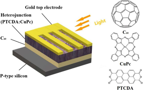
The schematic structure of devices based on hybrid planar-bulk heterojunction. The insets are molecular structures of PTCDA, CuPc and C60
Characterization of Devices
The absorption spectra of films were measured by using TU-1901 spectrometer. All measurements were performed using a semiconductor characterization system in a dark chamber at room temperature. Laser diodes with wavelengths of 405 nm, 450 nm, 532 nm, 655 nm and 808 nm were used as the light source, and the different optical powers were realized by using neutral density filters.
Results and Discussion
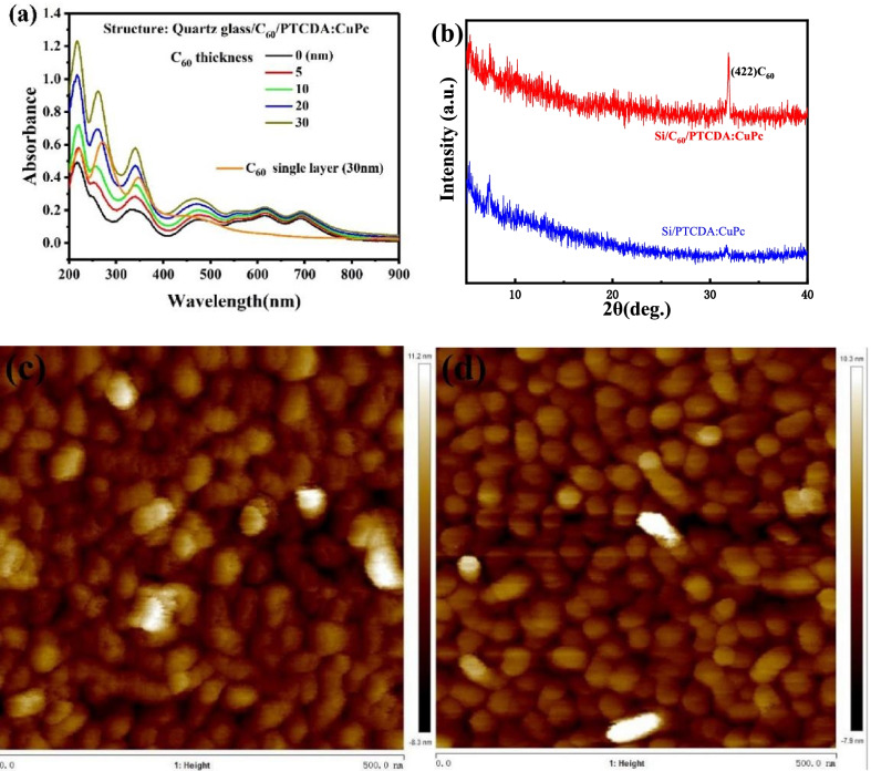
Figure 2a depict the optical absorption spectra of 30 nm-thick PTCDA:CuPc films on different thicknesses C60 films and C60 single layer. Here, the PTCDA:CuPc films show strong light absorption in the spectrum range of 200–400 nm and a uniform light absorption in the spectrum range of 450–700 nm. It is worth noting that a remarkably enhanced absorption was found from 200 to 500 nm when different thickness C60 films were inserted between the interface of the quartz glasses and PTCDA:CuPc films, which could be attributed to the absorption of C60 film dominates in the spectrum range of 200–500 nm. Figure 2b–d shows the XRD and AFM images of PTCDA:CuPc on 10 nm C60 film and single PTCDA:CuPc film. The double layer show an additional peak at 31.9°. As shown in the AFM images, the surface of the PTCDA:CuPc film is similar with or without the C60 layer. However, the roughness of the photosensitive film on the C60 layer is slightly higher. This shows that the addition of C60 does not significantly improve the performance of the device optically, or even not at all. Therefore, we believe that the improvement of device performance comes from the hole blocking effect of C60.
Fig. 2.
a Optical absorption spectra of C60 single layer (30 nm) and PTCDA:CuPc (30 nm) films deposited on C60 film of different thicknesses. All films were deposited on quartz glasses. b XRD spectrum of PTCDA:CuPc films with and without C60 film. And AFM images of c C60/PTCDA:CuPc and d PTCDA:CuPc films
The crystallite size (D) can be calculated by
| 1 |
where k is a constant, equal to 0.89, λ is X-ray wavelength of 0.15405 nm, β is full width at half maxima (FWHM) of diffraction peak, θ is diffraction angle. The FWHM of the peak at 2θ = 31.9 is 0.1617°. The calculated crystallite size is about 50 nm, which is consistent with the AFM image.
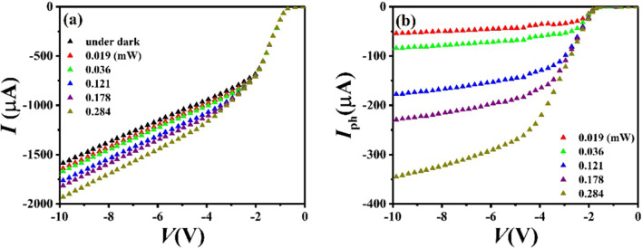
Figure 3a shows the typical I–V characteristics of the OIHPDs based on bulk heterojunction without C60 in the dark and under illumination of 532 nm laser. It is clear that the dark current is a bit large at a reverse bias voltage of − 10 V, which is as high as 1615.9 μA. The dependences of photocurrent on the reverse bias voltage are shown in Fig. 3b. It is seen that the photocurrent increases obviously with the incident optical power and gradually becomes saturated with reverse bias voltage increasing, which exhibits standard photodiode characteristics.
Fig. 3.
a The I–V characteristics of the device Si/PTCDA:CuPc (30 nm)/Au in the dark and under 532 nm laser illumination with different optical power. b The dependences of photocurrent on the reverse bias voltage under 532 nm laser illumination with different optical power
As an important parameter of photodetectors, the photoresponsivity (R) is defined as the value of the photocurrent (Iph) which generated in the external circuit under illumination of unit incident optical power (Pin), that is [39]
| 2 |
Another important parameter characterizing photodetectors is the specific detectivity (D*). Here we ignore the power spectral density of other noise sources such as flicker or thermal noise, it can be described as [40]
| 3 |
where q is the elementary electric charge, Jdark is the dark current density.
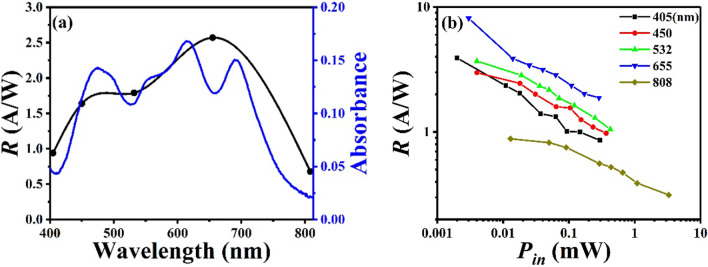
Figure 4a shows the dependence of photoresponsivity R on the wavelength at a reverse bias voltage of − 10 V and an incident optical power of ~ 0.1 mW. In the broad spectral response range from 405 to 808 nm, the responsivities of the OIHPD without C60 film (C60-free OIHPD) are all greater than 0.68 A/W. Especially, at the wavelength of 655 nm, the highest responsivity value is as high as 2.57 A/W. In addition, photoresponsivity generally follows the absorption spectrum of heterojunction films. As shown in Fig. 4b, under different wavelengths of light, the photoresponsivity decreased linearly with the incident light power increased in the logarithmic coordinate. Moreover, the maximal photoresponsivity is 8.13 A/W under 655 nm wavelength illumination with an incident optical power of 0.003 mW, and the minimal photoresponsivity is 0.32 A/W under 808 nm wavelength illumination with an incident optical power of 3.29 mW.
Fig. 4.
a The dependence of photoresponsivity R on the wavelength. b The logarithmic dependences of R on the incident optical power Pin. All results were obtained at a reverse bias voltage of − 10 V and an incident optical power of ~ 0.1 mW
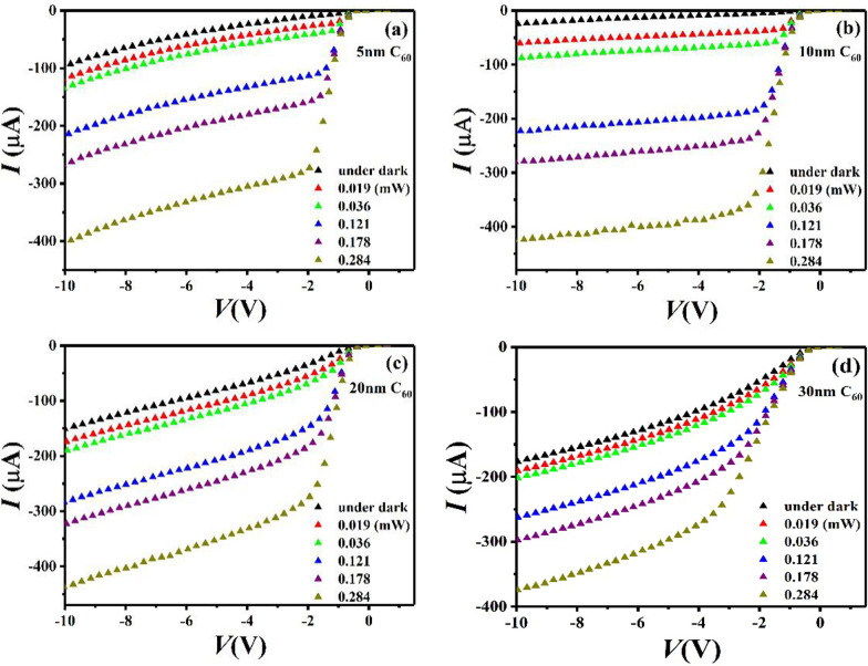
Figure 5 shows the I–V characteristics of the OIHPDs with different thicknesses C60 films (C60-OIHPDs) in the dark and under 532 nm laser illumination. All measurements were conducted in the same reverse bias voltage range with different incident optical power. It is observed that the dark currents were 92.1 μA (Fig. 5a), 25.6 μA (Fig. 5b), 149.0 μA (Fig. 5c) and 179.8 μA (Fig. 5d), which corresponded to the C60 thickness of 5 nm, 10 nm, 20 nm, 30 nm, respectively. Additionally, the C60-OIHPDs exhibited much lower dark current (Fig. 3a vs Fig. 5), and the minimum dark current of C60-OIHPDs was 25.6 μA when the C60 film thickness is 10 nm, which is about 63 times smaller than it of the C60-free OIHPD. Moreover, it is interesting to find that the dark current decreased first and then increased with increasing C60 thickness. Considering the energy level, a mechanism explanation as shown in Fig. 6 is proposed to support the phenomenon of the above OIHPDs. It is noteworthy that the energy levels of valence band (Ev) (5.24 eV) of p-type silicon, the highest occupied molecular orbital (HOMO) (5.3 eV) of CuPc and the work function of the gold electrode (5.1 eV) match well for hole transport in the absence of the C60 layer. Therefore, the holes can reach p-type silicon easily under a very low voltage bias, which causes a large dark current in the C60-free OIHPD. Fortunately, the HOMO (6.4 eV) of C60 is higher than the HOMO (5.3 eV) of CuPc, which means it will match better (Δ = 1.1 eV) for blocking hole transport. This is consistent with the experimental results that a high dark current of 1615.9 μA in the C60-free OIHPD and a low current of 25.6 μA in the C60-OIHPD. However, as an excellent electron transport material with high electron mobility (> 1.3 cm2 V−1 s−1) [41], a small amount of electrons can still easily reach the lowest occupied molecular orbital LUMO (4.2 eV) of C60 from the guide band Ec (4.05 eV) of p-type silicon. Thus, as the thickness of C60 film increasing, we infer that the injection of electrons is enhanced. In this regard, it has been reported that the strain relaxation in the multilayer film is related to the film thickness [42, 43]. Consequently, it is reasonable to assume that a thicker C60 film can provide broader space for the multilayer film, thereby more effectively alleviating the interplanar stress. In addition, the promotion of electron transport by the C60 film has become the dominant factor affecting dark current, which may be due to the increase of the dark current when the thickness of the C60 film exceeds 10 nm.
Fig. 5.
The I–V characteristics of the device Si/C60/PTCDA:CuPc (30 nm)/Au in the dark and under 532 nm laser illumination with different optical power. The thicknesses of C60 films are a 5 nm, b 10 nm, c 20 nm and d 30 nm, respectively
Fig. 6.
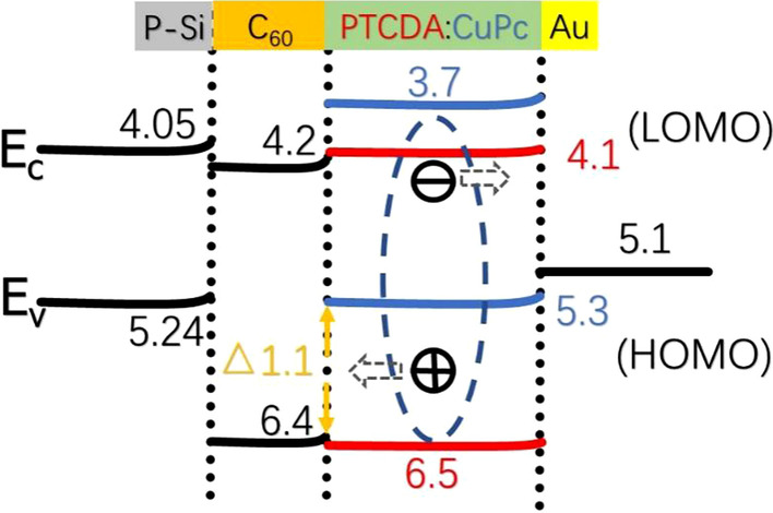
The energy level diagram and charge generation kinetics and transport mechanisms
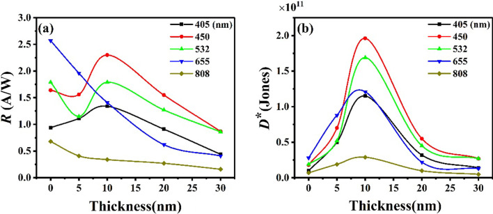
In order to better understand the effects of C60 thickness on device performance, the relationship curves about the dependences of photoresponsivity R on the thickness of C60 films is plotted in Fig. 7a. Under the wavelength of 405–532 nm, there is an overall trend that R firstly increased and then decreased with C60 thickness increasing, and the maximum value of R was reached with 10 nm thick C60 film. It is indicated that C60 film does enhance optional absorption from 200 to 500 nm, which is consistent with the absorption spectrum of C60 single layer (Fig. 2). But the thicker C60 film will also lead to smaller photocurrent and smaller R, this is probably because C60 film hinders the transmission of portion of the photogenerated carriers. As for the wavelength of 450–532 nm, R significantly decreased when the thickness of C60 increasing from 0 to 5 nm, we speculate that the inhibitory effect of the C60 film on the photocurrent is greater than the enhancement effect at this time. Under the wavelength of 655–808 nm, R decreased continuously as the thickness of C60 increasing, since the C60 film has no significant enhancement effect at the wavelength of 655–808 nm. Figure 7b shows the dependences of D* on the thickness for different wavelengths. The D* of device under different wavelengths illumination firstly increased with C60 thickness increasing and reach a maximum value at 10 nm, then decreased. The results above manifest that the optimized C60 thickness is 10 nm, which makes the D* reach the maximum. For the OIHPD with 10 nm C60 film (10 nm-C60 OIHPD), the D* over 1011 Jones in the wavelength range of 405–655 nm, and the highest D* value is 1.96 × 10¹¹ under the illumination of 450 nm wavelength. Compared with C60-free OIHPD, the D* of 10 nm-C60 OIHPD is almost one order of magnitude larger in the wavelength range of 405–808 nm (details in Table 1).
Fig. 7.
The dependences of a photoresponsivity R on the different C60 thicknesses, b specific detectivity D* on the thickness for different wavelengths. All results were obtained at a reverse bias voltage of − 10 V and an incident optical power of ~ 0.1 mW
Table 1.
Comparison of the photosensitive performance of broad spectral OIHPDs with different C60 thicknesses
| Device | |||||||||||
|---|---|---|---|---|---|---|---|---|---|---|---|
| C60 thickness | R (AW−1)a | D* (× 1011 Jones)a | Idark (μA)a | ||||||||
| Wavelength (nm) | 405 | 450 | 532 | 655 | 808 | 405 | 450 | 532 | 655 | 808 | |
| 0-nm | 0.94 | 1.64 | 1.79 | 2.57 | 0.68 | 0.10 | 0.18 | 0.19 | 0.28 | 0.07 | 1615.0 |
| 5-nm | 1.11 | 1.56 | 1.15 | 1.96 | 0.41 | 0.50 | 0.70 | 0.52 | 0.88 | 0.19 | 92.1 |
| 10-nm | 1.34 | 2.30 | 1.97 | 1.41 | 0.34 | 1.15 | 1.96 | 1.69 | 1.21 | 0.29 | 25.6 |
| 20-nm | 0.91 | 1.55 | 1.27 | 0.62 | 0.27 | 0.32 | 0.55 | 0.45 | 0.22 | 0.10 | 149.0 |
| 30-nm | 0.44 | 0.87 | 0.86 | 0.41 | 0.16 | 0.14 | 0.28 | 0.28 | 0.13 | 0.05 | 179.8 |
aAll results were obtained at a reverse bias voltage of − 10 V and an incident optical power of ~ 0.1 mW
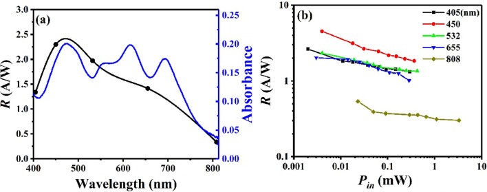
Figure 8a shows the dependence of photoresponsivity R on the wavelength for an incident optical power of ~ 0.1 mW at − 10 V. It is worth mentioning that the peak value of responsivity of 10 nm-C60 OIHPD changes to around 450 nm from 655 nm of C60-free OIHPD (Fig. 8a vs Fig. 4a) due to the addition of C60 film, which enhanced the absorption spectrum from 200 and 500 nm (Fig. 2). Furthermore, significantly reduced responsivity values are obtained at the wavelength of 655 nm and 808 nm (Fig. 8a vs Fig. 4a) due to C60 film which hinders the transmission of portion of the photo-generated carriers. As shown in Fig. 8b, it is seen that the 10 nm-C60 OIHPD has the best responsivity under the illumination of 450 nm because of the influence of C60 film. And the maximal responsivity is 4.53 A/W at an incident optical power of 0.004 mW of 450 nm, the minimal responsivity is 0.30 A/W at an incident optical power of 3.29 mW of 808 nm, respectively.
Fig. 8.
a The dependence of photoresponsivity R on the wavelength. b The logarithmic dependences of R on the incident optical power Pin. All results were obtained at a reverse bias voltage of − 10 V and an incident optical power of ~ 0.1 mW
Conclusion
In summary, the photodiodes based on hybrid planar-bulk heterojunction with different thicknesses C60 films were fabricated and characterized. The broad spectral region response from visible to near-infrared demonstrated that using C60 films as hole-blocking layer can effectively enhance the performance of broad spectral OIHPDs. Specifically, the OIHPD with 10 nm-C60 film exhibited the optimized performance with a much lower dark current of 25.6 μA, which is about 63 times smaller than that of C60-free OIHPD. A schematic energy level model combined with experimental measurements is well capable of explaining the origin of decreased dark current. Furthermore, the D* of the 10 nm-C60 OIHPD was almost one order of magnitude larger than the C60-free photodiode, and a notable enhancement of over 1011 Jones was obtained due to the fiercely reduced dark current.
Acknowledgements
Not applicable.
Abbreviations
- OIHPD
Organic–inorganic hybrid photodiode
- PTCDA
3,4,9,10-Perylenetertracarboxylic dianhydride
- CuPc
Copper phthalocyanine
- C60
Fullerene
- TAPC
1,1-Bis ((di-4-tolylamino) phenyl) cyclohexane
- EQE
External quantum efficiency
- D*
Specific detectivity
- R
Photoresponsivity
- XRD
Diffraction of x-rays
- FWHM
Full width at half maxima
- AFM
Atomic force microscope
Authors' contributions
ZZ: experiment, writing, GL: experiment, writing, XS: experiment, QD: experiment, LS: corresponding author, YP: corresponding author, PW: experiment instructor. All authors read and approved the final manuscript.
Funding
This work was supported by Natural Science Foundation of Zhejiang Province Grant No. LQ20F050008.
Availability of data and materials
The data in the manuscript were obtained from our measurements, so we will not share the data.
Declarations
Competing interests
The authors declare that they have no competing interests.
Footnotes
Publisher's Note
Springer Nature remains neutral with regard to jurisdictional claims in published maps and institutional affiliations.
Contributor Information
Lei Sun, Email: 17a0403150@cjlu.edu.cn.
Yingquan Peng, Email: yqpeng@cjlu.edu.cn.
References
- 1.Vijay J, Yadav RK, Alvi PA, Singh K, Rathi A (2020) Design and modeling of InGaAs/GaAsSb nanoscale heterostructure for application of optical fiber communication system. Mater Today Proc.
- 2.Rutz F, Bächle A, Aidam R, Niemasz J, Bronner W, Zibold A, Rehm R, Fulop GF, Hanson CM, Andresen BF (2019) InGaAs SWIR photodetectors for night vision. Infrared Technol Appl XLV 37
- 3.Ren D, Azizur-Rahman KM, Rong Z, Juang BC, Somasundaram S, Shahili M, Farrell AC, Williams BS, Huffaker DL. Room-temperature midwavelength infrared InAsSb nanowire photodetector arrays with Al2O3 Passivation. Nano Lett. 2019;19(5):2793–2802. doi: 10.1021/acs.nanolett.8b04420. [DOI] [PubMed] [Google Scholar]
- 4.Benavides CM, Biele M, Schmidt O, Brabec CJ, Tedde SF. TIPS Pentacene as a beneficial interlayer for organic photodetectors in imaging applications. IEEE Trans Electron Dev. 2018;65:1516–1522. doi: 10.1109/TED.2018.2799705. [DOI] [Google Scholar]
- 5.Lien MB, Liu CH, Chun IY, Ravishankar S, Nien H, Zhou M, Fessler JA, Zhong Z, Norris TB (2018) Ranging and light field imaging with transparent photodetectors. Nat Photon 1–6
- 6.Wang B, Zhong S, Ge Y, Wang H, Luo X, Zhang H. Present advances and perspectives of broadband photo-detectors based on emerging 2D-Xenes beyond grapheme. Nano Res. 2020;13(4):891–918. doi: 10.1007/s12274-020-2749-1. [DOI] [Google Scholar]
- 7.Xiao M, Mingyu L, Jian-Jun H. CMOS-compatible integrated spectrometer based on echelle diffraction grating and MSM photodetector array. IEEE Photon J. 2013;5:6600807–6600807. doi: 10.1109/JPHOT.2013.2250944. [DOI] [Google Scholar]
- 8.Shi L, Nihtianov S. Comparative study of silicon-based ultraviolet photodetectors. IEEE Sens J. 2012;12:2453–2459. doi: 10.1109/JSEN.2012.2192103. [DOI] [Google Scholar]
- 9.Xu GY, Salvador A, Kim W, Fan Z, Lu C, Tang H, Morkoç H, Smith G, Estes M, Goldenberg B, Yang W, Krishnankutty S. High speed, low noise ultraviolet photodetectors based on GaN p-i-n and AlGaN(p)-GaN(i)-GaN(n)structures. Appl Phys Lett. 1997;71:2154–2156. doi: 10.1063/1.119366. [DOI] [Google Scholar]
- 10.Kimukin I, Biyikli N, Butun B, Aytur O, Unlu MS, Ozbay E. InGaAs-based high-performance p-i-n photodiodes. IEEE Photonic Tech L. 2002;14:366–368. doi: 10.1109/68.986815. [DOI] [Google Scholar]
- 11.Yoshizawa A, Tsuchida H. A 1550 nm single-photon detector using a thermoelectrically cooled InGaAs avalanche photodiode. Jpn J Appl Phys. 2001;40:200–201. doi: 10.1143/JJAP.40.200. [DOI] [Google Scholar]
- 12.Li YN, Sonar P, Murphy L, Hong W. High mobility diketopyrrolopyrrole (DPP)-based organic semiconductor materials for organic thin film transistors and photovoltaics. Energy Environ Sci. 2013;6:1684–1710. doi: 10.1039/c3ee00015j. [DOI] [Google Scholar]
- 13.Katz HE, Lovinger AJ, Johnson J, Kloc C, Siegrist T, Li W, Lin YY, Dodabalapur A. A soluble and air-stable organic semiconductor with high electron mobility. Nature. 2000;404:478–481. doi: 10.1038/35006603. [DOI] [PubMed] [Google Scholar]
- 14.Costa JCS, Taveira RJS, Lima CFRAC, Mendes A, Santos LMNBF. Optical band gaps of organic semiconductor materials. Opt Mater. 2016;58:51–60. doi: 10.1016/j.optmat.2016.03.041. [DOI] [Google Scholar]
- 15.Dailey S, Feast WJ, Peace RJ, Sage IC, Till S, Wood EL. Synthesis and device characterisation of side-chain polymer electron transport materials for organic semiconductor applications. J Mater Chem. 2001;11:2238–2243. doi: 10.1039/b104674h. [DOI] [Google Scholar]
- 16.Rim YS, Yang YM, Bae SH, Chen H, Li C, Goorsky MS, Yang Y. Ultrahigh and broad spectral photodetectivity of an organic-inorganic hybrid phototransistor for flexible electronics. Adv Mater. 2015;27:6885–6891. doi: 10.1002/adma.201502996. [DOI] [PubMed] [Google Scholar]
- 17.Zhao F, Luo X, Liu J, Du L, Lv W, Sun L, Li Y, Wang Y, Peng Y. Toward high performance broad spectral hybrid organic–inorganic photodetectors based on multiple component organic bulk heterojunctions. J Mater Chem C. 2016;4:815–822. doi: 10.1039/C5TC03144C. [DOI] [Google Scholar]
- 18.Yang DZ, Zhou XK, Wang YP, Vadim A, Alshehri SM, Ahamad T, Ma DG. Deep ultraviolet-to-NIR broad spectral response organic photodetectors with large gain. J Mater Chem C. 2016;4:2160–2164. doi: 10.1039/C5TC04188K. [DOI] [Google Scholar]
- 19.Wang W, Zhao D, Zhang F, Li L, Du M, Wang C, Yu Y, Huang Q, Zhang M, Li L, Miao J, Lou Z, Shen G, Fang Y, Yan Y. Highly sensitive low-bandgap perovskite photodetectors with response from ultraviolet to the near-infrared region. Adv Funct Mater. 2017;27:1703953. doi: 10.1002/adfm.201703953. [DOI] [Google Scholar]
- 20.Han J, Yang D, Ma D, Qiao W, Wang ZY. Preparation of AZO:PDIN hybrid interlayer materials and application in high-gain polymer photodetectors with spectral response from 300 nm to 1700 nm. Org Electron. 2019;68:242–247. doi: 10.1016/j.orgel.2019.02.023. [DOI] [Google Scholar]
- 21.Ma L, Fan H, Tian H, Fang J, Qian X. The n-ZnO/n-In2O3 heterojunction formed by a surface-modification and their potential barrier-control in methanal gas sensing. Sens Actuators B Chem. 2016;222:508–516. doi: 10.1016/j.snb.2015.08.085. [DOI] [Google Scholar]
- 22.Zhang M, Fan H, Zhang N, Peng H, Ren X, Wang W, Li H, Chen G, Zhu Y, Jiang X, Wu P. 3D hierarchical CoWO4/Co3O4 nanowire arrays for asymmetric supercapacitors with high energy density. Chem Eng J. 2018;347:291–300. doi: 10.1016/j.cej.2018.04.113. [DOI] [Google Scholar]
- 23.Tian H, Fan H, Li M, Ma L. Zeolitic imidazolate framework coated ZnO nanorods as molecular sieving to improve selectivity of formaldehyde gas sensor. ACS Sens. 2016;1:243–250. doi: 10.1021/acssensors.5b00236. [DOI] [Google Scholar]
- 24.Huang F, Li Y, Xia H, Zhang J, Xu K, Peng Y, Liu G. Towards high performance broad spectral response fullerene based photosensitive organic field-effect transistors with tricomponent bulk heterojunctions. Carbon. 2017;118:666–674. doi: 10.1016/j.carbon.2017.03.091. [DOI] [Google Scholar]
- 25.Huang F, Wang X, Xu K, Liang Y, Peng Y, Liu G. Broadband organic phototransistor with high photoresponse from ultraviolet to near-infrared realized via synergistic effect of trilayer heterostructure. J Mater Chem C. 2018;6:8804–8811. doi: 10.1039/C8TC02148A. [DOI] [Google Scholar]
- 26.Peng Y, Huang F, Zhang J, Luo X, Xu K, Lv W, Xu S, Wang Y, Tang Y, Wei Y, Xu Z, Yang Y, Lu F. Broad spectral response photosensitive organic field-effect transistors realized by the hybrid planar-bulk heterojunction composed of three molecules with complementary optical absorption. Org Electron. 2017;43:27–32. doi: 10.1016/j.orgel.2017.01.008. [DOI] [Google Scholar]
- 27.Tchernycheva M, Guan N, Dai X, Messanvi A, Zhang H, Bayle F, Neplokh V, Piazz V, Julien FH, Bougerol C, Vallo M, Durand C, Eymery J (2016) Flexible optoelectronic devices based on nitride nanowires embedded in polymer films. In; IEEE nanotechnology materials and devices conference (NMDC), pp 1–2
- 28.Huang J, Du J, Cevher Z, Ren Y, Wu X, Chu Y. Printable and flexible phototransistors based on blend of organic semiconductor and biopolymer. Adv Funct Mater. 2017;27:1604163. doi: 10.1002/adfm.201604163. [DOI] [Google Scholar]
- 29.Pierre A, Arias AC (2016) High-detectivity printed organic photodiodes for large area flexible imagers. IEEE international electron devices meeting
- 30.Gelinck GH, Kumar A, Moet D, van der Steen JLPJ, van Breemen AJJM, Shanmugam S, Langen A, Gilot J, Groen P, Andriessen R, Simon M, Ruetten W, Douglas AU, Raaijmakers R, Malinowski PE, Myny K. X-ray detector-on-plastic with high sensitivity using low cost, solution-processed organic photodiodes. IEEE Trans Electron Devices. 2016;63:197–204. doi: 10.1109/TED.2015.2432572. [DOI] [Google Scholar]
- 31.Qian C, Sun J, Kong L-A, Gou G, Zhu M, Yuan Y, Huang H, Gao Y, Yang J. High-performance organic heterojunction phototransistors based on highly ordered copper phthalocyanine/para-sexiphenyl thin films. Adv Funct Mater. 2017;27:1604933. doi: 10.1002/adfm.201604933. [DOI] [Google Scholar]
- 32.Shekhar H, Solomeshch O, Liraz D, Tessler N. Low dark leakage current in organic planar heterojunction photodiodes. Appl Phys Lett. 2017;111:223301. doi: 10.1063/1.4996826. [DOI] [Google Scholar]
- 33.Ma C, Shi Y, Hu W, Chiu MH, Liu Z, Bera A, Li F, Wang H, Li LJ, Wu T. Heterostructured WS2/CH3NH3PbI3 photoconductors with suppressed dark current and enhanced photodetectivity. Adv Mater. 2016;28:3683–3689. doi: 10.1002/adma.201600069. [DOI] [PubMed] [Google Scholar]
- 34.Park S, Kim SJ, Nam JH, Pitner G, Lee TH, Ayzner AL, Wang H, Fong SW, Vosgueritchian M, Park YJ, Brongersma ML, Bao Z. Significant enhancement of infrared photodetector sensitivity using a semiconducting single-walled carbon nanotube/C60 phototransistor. Adv Mater. 2015;27:759–765. doi: 10.1002/adma.201404544. [DOI] [PubMed] [Google Scholar]
- 35.Li Y, Lv W, Luo X, Sun L, Zhao F, Zhang J, Zhong J, Huang F, Peng Y. Enhanced performance of PbPc photosensitive organic field effect transistors by inserting different-thickness pentacene inducing layers. Org Electron. 2015;26:186–190. doi: 10.1016/j.orgel.2015.07.042. [DOI] [Google Scholar]
- 36.Luo X, Du L, Wen Z, Lv W, Zhao F, Jiang X, Peng Y, Sun L, Li Y, Rao J. Remarkably enhanced red-NIR broad spectral absorption via gold nanoparticles: applications for organic photosensitive diodes. Nanoscale. 2015;7:14422–14433. doi: 10.1039/C5NR03308J. [DOI] [PubMed] [Google Scholar]
- 37.Yim C, McEvoy N, Riazimehr S, Schneider DS, Gity F, Monaghan S, Hurley PK, Lemme MC, Duesberg GS. Wide spectral photoresponse of layered platinum diselenide-based photodiodes. Nano Lett. 2018;18:1794–1800. doi: 10.1021/acs.nanolett.7b05000. [DOI] [PubMed] [Google Scholar]
- 38.Ni Z, Ma L, Du S, Xu Y, Yuan M, Fang H, Wang Z, Xu M, Li D, Yang J, Hu W, Pi X, Yang D. Plasmonic silicon quantum dots enabled high-sensitivity ultrabroadband photodetection of graphene-based hybrid phototransistors. ACS Nano. 2017;11:9854–9862. doi: 10.1021/acsnano.7b03569. [DOI] [PubMed] [Google Scholar]
- 39.Peng Y, Ding R, Ren Q, Xu S, Sun L, Wang Y, Lu F. High performance photodiode based on MoS2/pentacene heterojunction. Appl Surf Sci. 2018;459:179–184. doi: 10.1016/j.apsusc.2018.07.197. [DOI] [Google Scholar]
- 40.Lv W, Peng Y, Zhong J, Luo X, Li Y, Zheng T, Tang Y, Du L, Peng L. Near infrared sensitive organic photodiode utilizing exciplex absorption in NdPc2/C60 heterojunction. IEEE Photon Technol Lett. 2015;19:1–1. [Google Scholar]
- 41.Dong G, Zheng H, Duan L, Wang L, Qiu Y. High-performance organic optocouplers based on a photosensitive interfacial C60/NPB heterojunction. Adv Mater. 2009;21:2501–2504. doi: 10.1002/adma.200803152. [DOI] [Google Scholar]
- 42.Tamulevicius S. Stress and strain in the vacuum deposited thin films. Vacuum. 1998;51:127–139. doi: 10.1016/S0042-207X(98)00145-6. [DOI] [Google Scholar]
- 43.Abermann R. Measurements of the intrinsic stress in thin metal-films. Vacuum. 1990;41:1279–1282. doi: 10.1016/0042-207X(90)93933-A. [DOI] [Google Scholar]
Associated Data
This section collects any data citations, data availability statements, or supplementary materials included in this article.
Data Availability Statement
The data in the manuscript were obtained from our measurements, so we will not share the data.


