Abstract
Molybdenum disulfide (MoS2) was grown on a laser-processed periodic-hole sapphire substrate through chemical vapor deposition. The main purpose was to investigate the mechanism of MoS2 growth in substrate with a periodic structure. By controlling the amount and position of the precursor, adjusting the growth temperature and time, and setting the flow rate of argon gas, MoS2 grew in the region of the periodic holes. A series of various growth layer analyses of MoS2 were then confirmed by Raman spectroscopy, photoluminescence spectroscopy, and atomic force microscopy. Finally, the growth mechanism was studied by transmission electron microscopy (TEM). The experimental results show that in the appropriate environment, MoS2 can be successfully grown on substrate with periodic holes, and the number of growth layers can be determined through measurements. By observing the growth mechanism, composition analysis, and selected area electron diffraction diagram by TEM, we comprehensively understand the growth phenomenon. The results of this research can serve as a reference for the large-scale periodic growth of MoS2. The production of periodic structures by laser drilling is advantageous, as it is relatively simpler than other methods.
Keywords: chemical vapor deposition, periodic growth of MoS2, growth mechanism of MoS2, Molybdenum disulfide (MoS2)
1. Introduction
One of the most important two-dimensional (2D) transition metal chalcogenides that is gaining increased attention is MoS2 [1,2,3,4,5,6,7]. Materials with nanoscale electronic and optoelectronic components, such as field-effect transistors, prospective memory components, light-emitting diodes, and sensors, have been manufactured by exploiting the excellent spin–valley coupling and flexural and optoelectronic properties of MoS2 [8,9,10,11,12,13,14,15,16,17,18,19,20]. Two-dimensional MoS2 is low cost and does not require complex preparation [21]. To date, MoS2-based semiconductor heterostructures, such as CdS/MoS2, MoO3/MoS2, and SnO2/MoS2, featuring good photocatalytic or photoelectrochemical properties, have been successfully synthesized owing to the efficient charge separation obtained by coupling two semiconductor structures with matched energy levels [22,23,24,25]. Nevertheless, the mass production of such devices demands a method of synthesizing large-scale, layer-controlled, high-quality MoS2. Most studies on MoS2 films with excellent results have been obtained using a top-down approach, such as mechanical exfoliation [26,27]. Other studies are moving from characterizing 2D thin films to manufacturing low-cost devices, mass producing logic-integrated circuits, and growing 2D materials on foreign substrates. They aim to replace the existing exfoliation and liquid exfoliation methods for producing randomly distributed flakes and providing limited control of the number of MoS2 film layers. Chemical vapor deposition (CVD) is the usual vapor-phase growth method used to create semiconductor thin films and heterojunctions [28]. CVD is gaining increased attention owing to its success in the growth of large-area, high-quality, and uniform nanofilms [29,30,31,32,33]. In the present work, MoS2 was grown on a laser-processed periodic-hole sapphire substrate through the CVD method. We aimed to analyze the growth mechanism of MoS2 with a regular structure by controlling the amount and location of the precursor, modifying the growth temperature and time, and setting the flow rate of argon gas (Ar) to induce MoS2 growth around the periodic holes.
2. Materials and Methods
2.1. Preparation of Laser Drilling for Substrates Containing Periodic Structures
The most direct way to prepare many periodic patterned microstructures is to prepare traces on the substrate surface and to use laser processing to drill holes with about 10 μm diameter and 300 nm depth. Laser drilling damages the substrate structure and causes unevenness around the hole, which has a certain degree of influence on the MoS2 growth mechanism.
2.2. Growth of MoS2 on Sapphire Substrate by CVD
The substrate used to grow MoS2 was sapphire with silicon dioxide (SiO2) on the surface (see Supplementary Materials Section 1 for obtaining the MoS2 layers). Periodic holes were made by laser processing, and then CVD was performed. The precursors used were sulfur powder (S) with a purity of 99.98% and molybdenum oxide powder (MoO3) with a purity of 99.95%. High-purity chemical powders were used to remove impurities remaining in the experimental cavity and affecting the CVD. It was also possible to grow single crystals with residual impurities. The chemical solvent used to clean the remaining chemical substances after each experiment was aqua regia. The concentrations of nitric acid and hydrochloric acid (HCl) used to prepare aqua regia were 37 vol.% and 68–69 vol.%, respectively. The quartz tube and ceramic crucible were cleaned inside the tubular thermal furnace with this solution (see Supplementary Materials Section 2.6 for tube furnaces). The quartz tube was regularly replaced according to the change in residual sulfur powder on the tube wall. The purpose was to reduce the impact of experimental environmental factors. The substrates, organic solvents, gases, and chemicals used are detailed in Table 1.
Table 1.
List of substrates, organic solvents, gases, and chemicals used for MoS2.
| S powder | Weiss Enterprise |
| MoO3 powder | Weiss Enterprise |
| Nitric acid | CHONEYE |
| Hydrochloric acid | FLUKA |
| Sapphire substrate | Vertex Co., Ltd. |
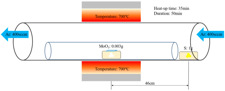
Before the start of the experiment, the cleanliness of the substrate was confirmed (Supplementary Materials Section 2). First, 1 g of sulfur and 0.003 g of MoO3 were prepared and placed in appropriate positions in the inner tube of the quartz tube. The substrate was set inverted on molybdenum trioxide (MoO3). The inert gas used during growth was Ar. Initially, 500 sccm of Ar was let in for 10 min to clean the internal cavity. More water and oxygen were removed in the quartz tube, after which, the Ar flow was reduced to 200 sccm. The heating rate was set to 20 °C/min. The maximum temperature was set to 700 °C, and the heating time was set to 35 min. After reaching the maximum temperature, the same was maintained for 50 min. Finally, once the temperature dropped to <400 °C, it was further dropped to room temperature by opening the lid, and the MoS2 structure was obtained. The experimental process is shown in Figure 1.
Figure 1.
Flow chart of MoS2 growth by CVD.
Considering that the vaporization point of MoO3 is above 650 °C and the vaporization point of S is above 200 °C, MoO3 in the gas phase underwent two chemical reactions in high-temperature environments to produce the intermediate molybdenum oxide (MoO3−x). This intermediate molybdenum oxide diffused to the substrate and reacted with vaporized sulfur to form MoS2 film. The distance between the two crucibles containing the precursor was 46 cm. Single-layer and multilayer MoS2 can be effectively prepared by CVD, as shown in the following equations:
| MoO3(s) + H2(g) → MoO2 + H2O(g) |
| MoO2(s) + 2S(g) → MoS2(s) + O2(g) |
2.3. Growth Mechanism of MoS2
The properties of MoS2 are useful for semiconductors and optoelectronic materials with single or few layers. CVD is the most commonly used method for MoS2 growth. Given that the location of CVD growth of single-layer MoS2 is relatively random, understanding its growth mechanism can substantially benefit research on MoS2 growth. TEM helps elucidate the atomic structure and the chemical composition information of particle evolution during catalysis [34,35,36,37,38,39,40]. The material properties of MoS2 are preferably a single layer or very few layers. The analysis of the number of layers depended on the Raman spectra, atomic force microscopy (AFM) images, and photoluminescence (PL) spectra (see Supplementary Materials Section 2.1 for micro-Raman spectroscopy; see Supplementary Materials Section 2.2 for micro-Raman micro-PL spectrometer). Raman measurements were made using a laser with a wavelength of 532 nm as the excitation light source. TEM can also be used to measure the number of observation layers of the substrate cross-section (see Supplementary Materials Section 2.7 for transmission electron microscope). The multilayer structure in the cross-section geometry was studied by TEM using lamella specimens produced by focused ion beam (FIB) milling. The phase state of the multilayer volume was assessed by selected area electron diffraction (SAED) pattern analyses and fast Fourier transform (FFT) patterns generated from the corresponding regions of the HRTEM images (see Supplementary Materials Section 3 for TEM analysis).
3. Results
3.1. CVD Growth of Periodic MoS2
The CVD method is used to grow MoS2, and a substrate with periodic holes is prepared by laser drilling in a high-temperature furnace tube to grow MoS2.
3.1.1. Image Analysis under Optical Microscopy (OM)
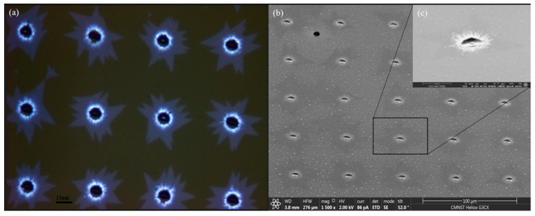
Many methods are well established to identify the number of MOS2 layers, but in this study, an optical microscope was used (Supplementary Materials Section 2.3, optical microscope) [41,42,43,44,45,46]. OM reveals the growth pattern of MoS2. Figure 2 shows the OM and SEM images of MoS2 grown on a sapphire substrate.
Figure 2.
(a) OM image, (b) SEM image, and (c) partial enlarged view of (b) showing the periodic growth of MoS2 on sapphire substrate.
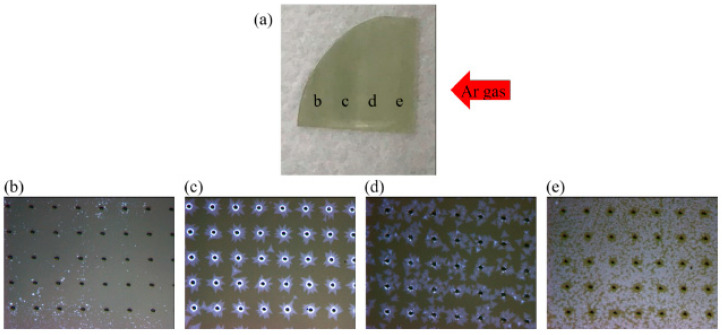
Figure 3a is an image of the substrate after actual growth. The red arrow indicates the direction of Ar flow during CVD. The growth distributions of different MoS2 shapes are shown as the marked locations b, c, d, and e. Figure 3b is the OM image at position b in Figure 3a, where the black holes are the result of the original laser processing, and the blue points are the areas where MoS2 grows. Figure 3c is the OM image at position c in Figure 3a, where MoS2 grows regularly in the hole area, with a bright blue ring pattern on the edge of the hole. This finding shows the existence of a multilayer MoS2. The light blue irregular shape distribution on the periphery of the hole is represented by the existence of single-layer MoS2. Figure 3d is the OM image at position d in Figure 3a, where we can see that a single layer of MoS2 grows along the hole periphery. The periodic growth is not as good as that at the c position, but the single-layer MoS2 covers a large area with no high-level MoS2. Figure 3e is the OM image at position e in Figure 3a, where we can see that the single layer of MoS2 grows in a more broken manner on the substrate and covers a larger area, but no MoS2 exists around the hole. These results show that according to the Ar flow direction, MoS2 grows in the order of large to small coverage area and from a broken and to a more regular growth around the hole until it no longer exists. Thus, we infer that the MoS2 growth is cyclical.
Figure 3.
(a) Image of sapphire substrate after MoS2 growth. (b) OM image at position b in (a). (c) OM image at position c in (a). (d) OM image at position d in (a), and (e) is the OM image at position e in (a).
3.1.2. Raman Spectrum Analysis Results
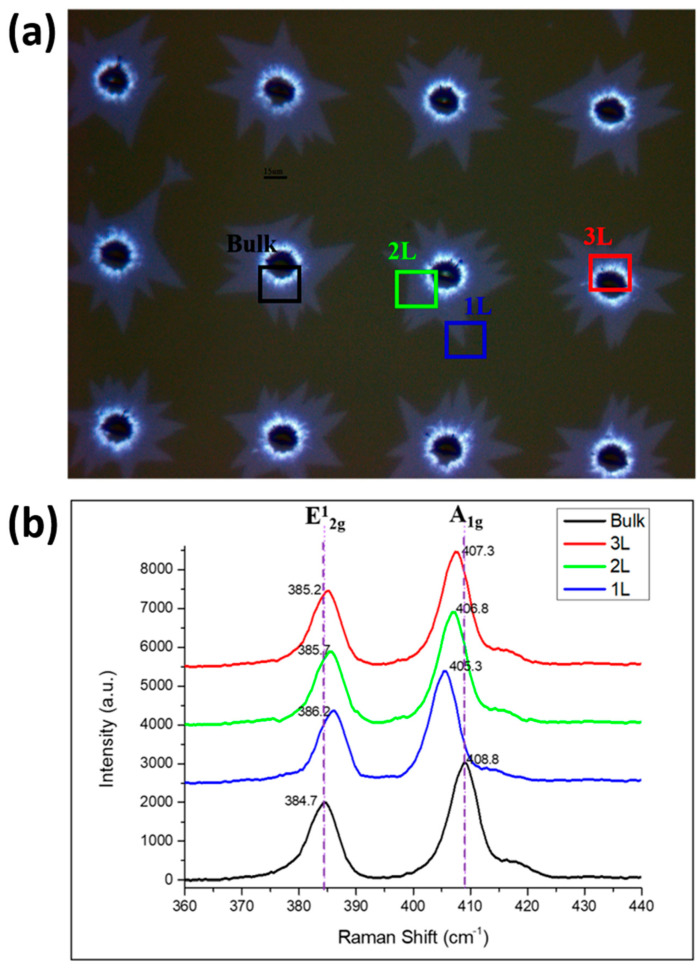
Raman mapping, which is the best method for analyzing the number of layers, is used to analyze the image [47,48,49,50]. The results reveal that MoS2 has two peaks at 380 and 400 cm−1, respectively. When the difference (Δk) between the two peaks is less than 20 cm−1, it is a single-layer MoS2 structure. The peak is attributed to the in-plane (E12g) and out-of-plane (A1g) oscillation modes of MoS2.
Figure 4a shows an OM image of MoS2 periodic growth. The black, blue, green, and red boxes indicate the areas where multilayer and one-, two-, and three-layer MoS2 growth are measured, respectively. Figure 4b shows the Raman measurement diagram of each area marked in Figure 5a. The black part demonstrates that the Raman shift is between 384.7 and 408.8 cm−1, and the value of the peak difference (Δk) is 24.1 cm−1. This finding indicates more than four layers, which is unsuitable for semiconductor components and optoelectronic components. The blue part shows that the peak difference between the Raman shift of 386.2 and 405.3 cm−1 is 19.1 cm−1, which represents a single layer. In the green part, we find that the peak difference between the Raman shift of 385.7 and 406.8 cm−1 is 21.1 cm−1, defined as a two-layer growth of MoS2. In the red part, we find that the peak difference between the Raman shift of 385.2 and 407.3 cm−1 is 22.1 cm−1, defined as three layers of MoS2. The Raman measurements prove that the periodicity of our growth has one- to three-layer and multilayer characteristics. These findings prove that MoS2, which grows periodically in the hole, has different distributions from single to multiple layers and, thus, has multiple potential applications. The areas of few-layered MoS2 are sufficiently large. Thus, it is highly applicable in semiconductor device manufacturing.
Figure 4.
Panel (a) is an OM image of MoS2 periodic growth, whereas (b) is the Raman measurement diagram of each area marked in (a).
Figure 5.
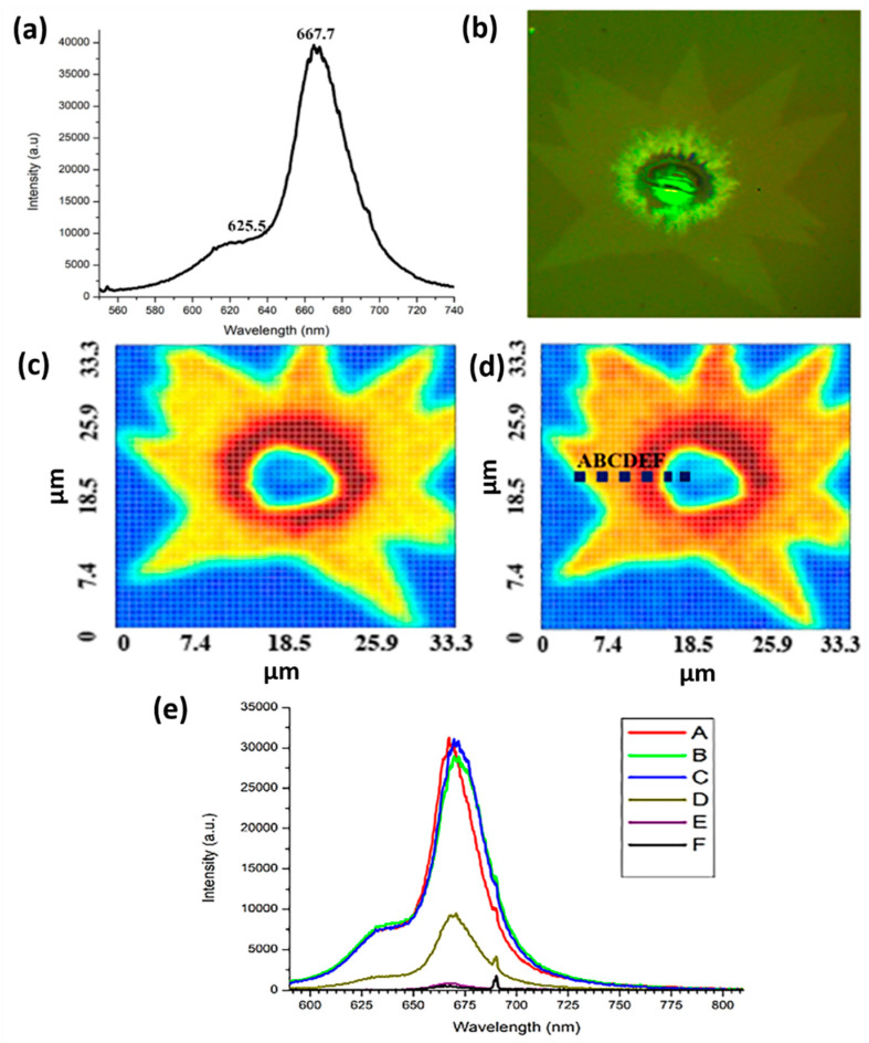
(a) PL measurement results of MoS2 sample. (b) OM image of the selected PL mapping range. (c,d) PL mapping at 625 and 667 nm. (e) PL measurement result of the test piece marked by the blue dotted line in (d).
3.1.3. PL Spectrum Analysis Results
Figure 5a shows the result of the PL analysis of the MOS2 sample. Obvious luminescence peaks exist at about 625 and 667 nm, indicating that MoS2 is in a single layer and a few layers, respectively. Each layer corresponds with the valence band spin–orbit coupling splitting of MoS2 direct exciton transition luminescence (B exciton) and direct energy gap recombination luminescence (A exciton). The converted energy is about 1.98 and 1.86 eV, respectively. We infer that this structure is single-layer MoS2. Figure 5b shows the OM image of the selected PL mapping range. The greenish color is due to the light source of the instrument. Figure 5c shows the PL mapping diagram of the selected PL mapping range OM image with a wavelength of 625 nm in Figure 5b. The blue part is the sapphire substrate, and the yellow to red is the distribution from single layer to multilayer. The blue part is the sapphire substrate, and the yellow-orange to red is the distribution from single layer to multilayer. The dashed parts A and F correspond with the grid points of the X-axis position of the different color curves in Figure 5d. The color line segments A–F in the upper right corner represent the number of grids selected in the X-axis direction of the mapping grid number 37 × 37 in Figure 5d. The positions of the line segments with higher strength are A, B, and C. A higher number of layers of growing MoS2 corresponds with decreased strength, as shown in positions D, E, and F. From the results of the PL spectrum analysis, we infer from the mapping image presented by the excitation light peaks at 625 and 667 nm that the periodic growth of MoS2 has good uniformity in the distribution of monolayer to multilayer.
3.1.4. Selected Area Electron Diffraction
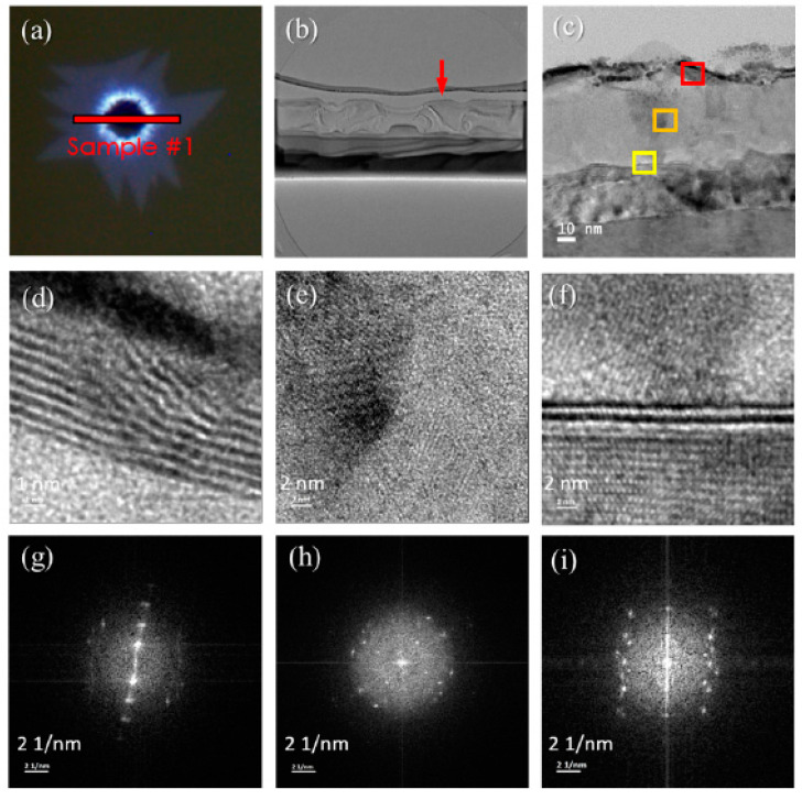
From the composition analysis, we can infer the mechanism of the periodic growth of MoS2. We use the additional function of the TEM system to convert the diffraction image of the selected area into a lattice arrangement through FFT. The red line in Figure 6a indicates the FIB sampling position (see Supplementary Materials Section 2.5 for dual-beam FIB). Figure 6g is the SAED image of Figure 6d, with a miller index of [001]. In this direction, we can see the multilayer-structured MoS2 lattice array. The distance between the layers reveals the hexagonal crystal structure of MoS2 with lattice constants a = 0.318 nm and c = 1.299 nm. Moreover, the crystal plane distance between the multilayer MoS2 layer is 6.2 A, which is close to the 2-H MoS2 crystal plane distance of about 6.5 A. Figure 6h is the SAED image of Figure 6e. The miller index is [001], which shows that the lattice arrangement is chaotic, but the faint lattice points in the four directions may be MoO3. Figure 6i is the SAED image of Figure 6f. The miller index is still [001], and the selected area is the junction of the mixed area and the sapphire substrate at the obvious double layer of HRTEM. Given that the boundary may diffract from the lattice of the upper and lower components of the boundary, it is more mixed. However, from the center point, the miller index [001] can be found, and the distance between the crystal planes is calculated to be about 6.4 Å.
Figure 6.
Panel (a) is the OM image after growing MoS2, (b) is the cross-sectional TEM image of the selected area in (a), (c) is the enlarged TEM image of the red arrow in (b). Panels (d–f) represent the HRTEM images of the red, orange, and yellow boxes in (c), respectively, and (g–i) represent the SAED diagrams in (d–f), respectively.
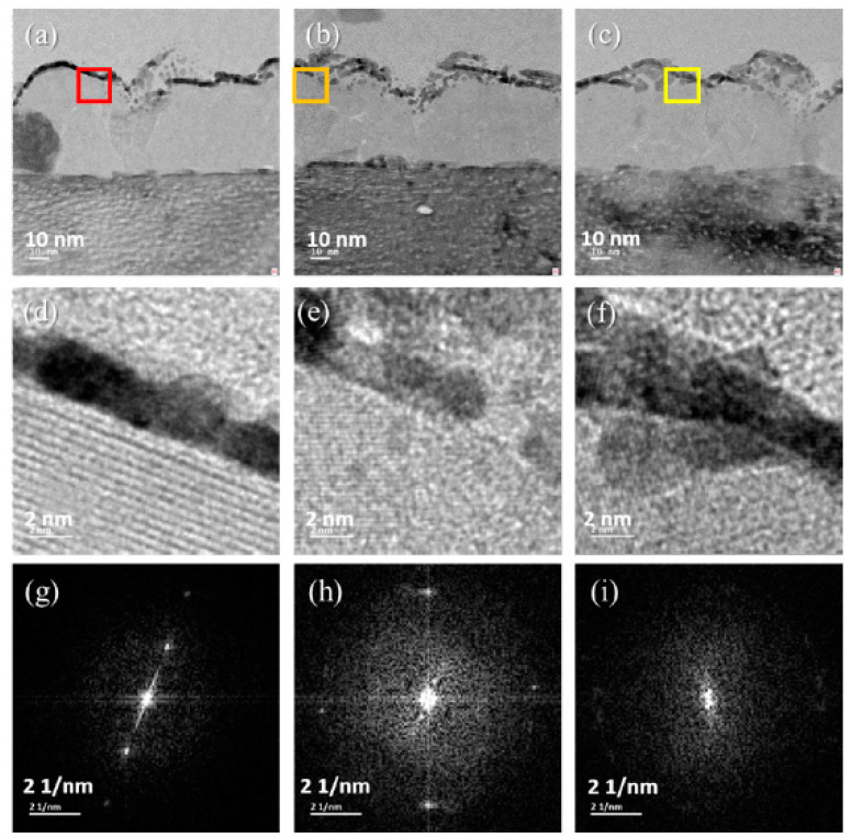
Sample 2 is analyzed using the TEM image defined in Figure 7. The sampling position does not pass through the hole. The growth of MoS2 on the surface is analyzed, as shown in Figure 7. Figure 7a shows the TEM image of the Sample 2 sampling location A, and the red box is the sampling location mark. Figure 7b shows the TEM image of the Sample 2 sampling location B, and the orange box is the sampling location mark. Figure 7c shows the TEM image of the Sample 2 sampling location C, and the yellow box is the sampling location mark. Figure 7d shows the HRTEM image of the red box in Figure 7a. The multilayer growth of MoS2 is stacked layer by layer. Figure 7e shows the HRTEM image, where the orange box in Figure 7b is a mixed area, and no MoS2 is observed. Figure 7f is the yellow box in Figure 7c. In the HRTEM image, the mixed zone is shown in the image. Figure 7g is the SAED diagram of Figure 7d, and the miller index is [001]. Here, the lattice arrangement can be seen as multilayer MoS2. Figure 7h is the SAED diagram of Figure 7e. The miller index is [001], and the main composition seen is MoO3. Figure 7i is the SAED diagram of Figure 7f, and the miller index is [001]. The image diffracted from the single-layer MoS2 viewed from this miller index is a lattice point, which may be interpreted as a single-layer MoS2 lattice. Based on the results of the SAED diagram analysis, we can determine from the lattice array that the grown MoS2 material is consistent with the compound calculated using the element ratio. We can interpret that 2-H MoS2 forms under the growth mechanism.
Figure 7.
Panels (a–c) represent the TEM images of Sample 2 in sampling locations A, B, and C, respectively; (d–f) represent the HRTEM images of the red, orange, and yellow boxes in (a–c), respectively; and (g–i) represent the SAED diagram in (d–f), respectively.
4. Discussion
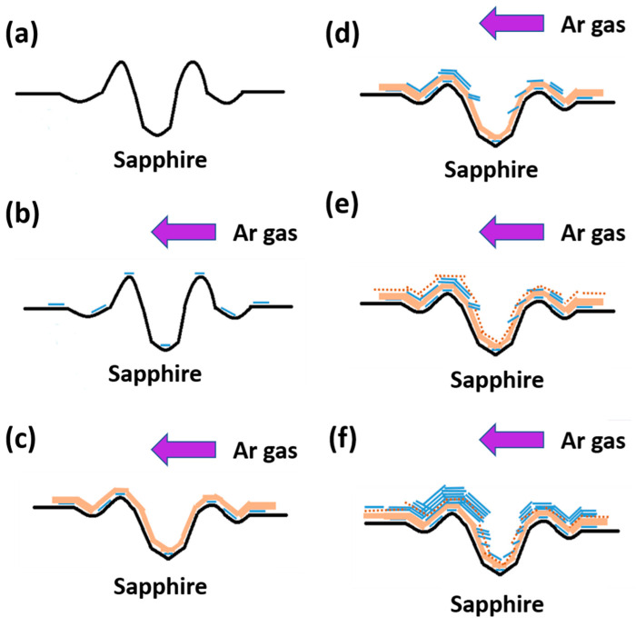
Figure 8 is a flow chart of the MoS2 growth process with periodic holes. Figure 8a shows the surface undulation curve of the substrate with periodic holes on ungrown MoS2. The blue line at the top of Figure 8b is the initial stage of growth. A single layer of MoS2 forms when S is dominant, and the purple arrow above represents the direction of Ar. The light brown area in Figure 8c is the mixed region generated when MoO3 is dominated. The composition contains Al2O3, MoO3, and MoS2. Figure 8d shows that when S becomes dominant during the growth period, a single layer or multiple layers of MoS2 are deposited. Although MoS2 grows and overlaps in a curved sheet shape, on the steeper edge of the hole, the sheet-shaped MoS2 grows with the growth side facing upward. In Figure 8e, the brown dashed line indicates the mixed area covered by MoO3 once again during the growth period. Figure 8f is the schematic at the end of the growth. The line segment overlapping on the top represents multiple layers. MoS2 particles overlap with one another in a flake shape. The air flow is thicker after the hole in the direction than before the hole, as seen from the MoS2 on the top. Finally, MoO3 is nearly depleted, and S eventually dominates the final stage of CVD growth. This phenomenon is related to the experimental setting of 0.003 and 1 g of S.
Figure 8.
Schematic of the growth process of MoS2. The purple arrow in the figure is the direction of argon ventilation, the blue line segment represents a single layer of MoS2, the light yellow area represents the mixed zone dominated by MoO3, the dark yellow dot is amorphous Al2O3 mixed in the reflection, and the blue line segment is superimposed to represent multilayer MoS2.
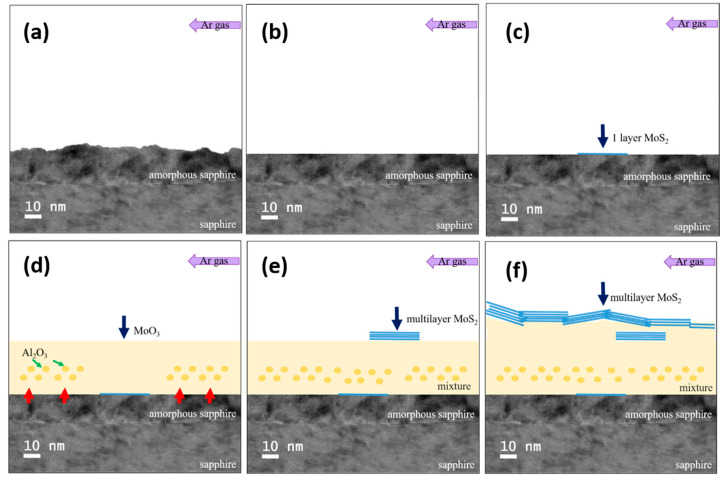
Figure 9 is a schematic of the growth process of MoS2, and Figure 9a is a schematic before growth. The upper layer of the lower sapphire substrate is an amorphous state damaged by laser processing. In Figure 9b, the blue arrow indicates the single layer of MoS2 grown on the substrate surface at the initial stage of growth. In Figure 9c, the blue arrow indicates the coverage of MoO3 at the middle stage of growth, and the green arrow indicates the Al2O3 surface layer at the same time, showing that it mixed at a high temperature to form a mixture zone. The blue arrow in Figure 9d indicates the formation of multiple layers of MoS2, indicating that S gas is greater than MoO3 gas during this growth period. Figure 9e is the schematic of the growth end, and the blue arrow indicates that multiple layers of MoS2 grow to be stacked in sheets. Although in this study, MoS2 is grown on a laser-processed periodic-hole sapphire substrate through CVD, to integrate the developed MoS2 films into practical tools and nanostructures, various patterning and interfacing approaches have been developed. Post-patterning approaches have been successful, indicating wide-ranging applications in current microelectronic techniques, such as FIB milling, photo- and electron-beam lithography, and combinations of metal sputtering processes with selective etching after photolithographically defined masking [51,52,53,54].
Figure 9.
Schematic of the MoS2 growth process. The purple arrow in the figure is the direction of argon ventilation, and the blue line segment represents a single layer of MoS2. The light yellow area represents the mixed zone dominated by MoO3, the dark yellow dot is amorphous Al2O3 mixed in the reflection, and the blue line segment is superimposed to represent multilayer MoS2.
5. Conclusions
We used a femtosecond laser to prepare a periodic array of holes with a diameter of about 10 μm on a single-sided polished sapphire substrate. The substrate is grown by CVD of MoS2, and the layer is successfully grown. This technique can be used for growth multiple times, and the results reveal that the size, shape, and number of layers of MoS2 grown each time are different. The possible reason is that the experiment proceeds under atmospheric pressure. Creating a system completely isolated from external interference is impossible, and the influence of external environmental factors on the growth results cannot be predicted. However, other possible causes can be minimized by cleaning the experimental cavity, as well as ensuring minimal differences in parameters and the distance between each substrate installation. The growth mechanism is observed and analyzed using Raman, PL, and AFM analyses to confirm the distribution of the number of generated layers. They are found to possess single- and few-layer positions with excellent photoelectric and semiconductor properties. TEM is used to observe and analyze the cross-sectional image, and the extended function of the TEM is adopted to analyze and convert the SAED image. Subsequently, the growth mechanism is comprehensively analyzed. From the results, we can infer that in a large area of the substrate, MoS2 growth increases and breaks with the direction of Ar until it is concentrated and periodically attaches around the holes, but not at the very end. For the same periodic hole in a small area, MoS2 growth occurs by overlapping pieces, and the number of layers is distributed from the thickest ring around the hole to the single layer at the corner of MoS2. After understanding this growth mechanism, we can select the part of the substrate to be used and the number of layers of MoS2 according to the requirements of the components to be manufactured.
Supplementary Materials
The following supporting information can be downloaded at: https://www.mdpi.com/2079-4991/12/1/135/s1, Figure S1. (a) An image of a sapphire substrate with periodically growing MoS2. (b) Partially enlarged image of (a). (c) Enlarged OM image of the red box in (b). Figure S2. (a) OM image of MoS2 periodic growth. (b) SEM image of the cross-section of (a) marked by the red line, defined as Sample 1. (c) SEM image of the cross-section at Sample 2, where the red line marks the sampling defined as Sample 2 in (a). Figure S3. (a) A cross-sectional SEM image of Sample 1. (b) Schematic of the nomenclature of the section in (a). Figure S4. (a) Schematic of the cross-section of Sample 1. (b) HRTEM image of the red arrow in (a). (c) HRTEM image of the green arrow in (a). (d) HRTEM image of the blue arrow in (a). Figure S5. (a) Schematic of the cross-section of Sample 1. (b) HRTEM image of the red arrow in (a). (c) HRTEM image of the green arrow in (a). (d) HRTEM image of the blue arrow in (a). Figure S6. (a) Schematic of the cross-section of Sample 1. (b) HRTEM image of the red arrow in (a). (c) HRTEM image of the green arrow in (a). (d) HRTEM image of the blue arrow in (a). Figure S7. (a) Schematic of the cross-section of Sample 1. (b) HRTEM image of the red arrow in (a). (c) HRTEM image of the green arrow in (a). (d) HRTEM image of the blue arrow in (a). Figure S8. (a) Schematic of the cross-section of Sample 1. (b) HRTEM image of the red arrow in (a). (c) HRTEM image of the blue arrow in (a). Figure S9. (a) TEM image of the cross-section of the substrate without periodic MoS2 holes. (b) TEM image of the cross-section of the substrate with MoS2 periodic holes. Figure S10. (a) HRTEM image of the cross-section of the substrate with periodic holes in MoS2. The boxed area is where EDS analysis was performed. (b) EDS analysis image and data of the red boxed area in (a). (c) EDS analysis graph and data of the orange box in (a). (d) EDS analysis graph and data of the yellow box in (a). (e) EDS analysis diagram and data of the green box in (a). (f) EDS analysis and data of the blue box in (a).
Author Contributions
Conceptualization, V.E.F., Y.-M.T., H.-C.W. and S.B.A.; methodology, A.M., H.-C.W., S.B.A. and Y.-M.T.; software, S.B.A., V.E.F., H.-C.W. and A.M.; validation, Y.-M.T., V.E.F., S.B.A. and H.-C.W.; formal analysis, Y.-M.T., V.E.F. and H.-C.W.; investigation, Y.-M.T., V.E.F. and S.B.A.; resources, Y.-M.T., V.E.F. and H.-C.W.; data curation, A.M., H.-C.W., S.B.A. and S.B.A.; writing—original draft preparation, A.M.; writing—review and editing, A.M. and H.-C.W.; supervision, H.-C.W.; project administration, H.-C.W. All authors have read and agreed to the published version of the manuscript.
Funding
This research was supported by the Ministry of Science and Technology, The Republic of China, under grants MOST 105-2923-E-194-003 MY3, 108-2823-8-194-002, 109-2622-8-194-001-TE1, 109-2622-8-194-007, and 110-2634-F-194-006. This work was financially/partially supported by the Advanced Institute of Manufacturing with High-tech Innovations and the Center for Innovative Research on Aging Society from The Featured Areas Research Center Program within the framework of the Higher Education Sprout Project by the Ministry of Education in Taiwan.
Conflicts of Interest
The authors declare no conflict of interest.
Footnotes
Publisher’s Note: MDPI stays neutral with regard to jurisdictional claims in published maps and institutional affiliations.
References
- 1.Geim A.K., Novoselov K.S. The rise of graphene. Nat. Mater. 2007;6:183–191. doi: 10.1038/nmat1849. [DOI] [PubMed] [Google Scholar]
- 2.Das Sarma S., Adam S., Hwang E.H., Rossi E. Electronic transport in two-dimensional graphene. Rev. Mod. Phys. 2011;83:407–470. doi: 10.1103/RevModPhys.83.407. [DOI] [Google Scholar]
- 3.Lin X., Su L., Si Z., Zhang Y., Bournel A., Zhang Y., Klein J.-O., Fert A., Zhao W. Gate-Driven Pure Spin Current in Graphene. Phys. Rev. Appl. 2017;8:034006. doi: 10.1103/PhysRevApplied.8.034006. [DOI] [Google Scholar]
- 4.Wu C., Zhang J., Tong X., Yu P., Xu J.Y., Wu J., Wang Z.M., Lou J., Chueh Y.L. A critical review on enhancement of photocatalytic hydrogen production by molybdenum disulfide: From growth to interfacial activities. Small. 2019;15:1900578. doi: 10.1002/smll.201900578. [DOI] [PubMed] [Google Scholar]
- 5.Yang D., Wang H., Luo S., Wang C., Zhang S., Guo S. Cut Flexible Multifunctional Electronics Using MoS2 Nanosheet. Nanomaterials. 2019;9:922. doi: 10.3390/nano9070922. [DOI] [PMC free article] [PubMed] [Google Scholar]
- 6.Zhang Y., Wan Q., Yang N. Recent Advances of Porous Graphene: Synthesis, Functionalization, and Electrochemical Applications. Small. 2019;15:1903780. doi: 10.1002/smll.201903780. [DOI] [PubMed] [Google Scholar]
- 7.Li K.-C., Lu M.-Y., Nguyen H.T., Feng S.-W., Artemkina S.B., Fedorov V.E., Wang H.-C. Intelligent Identification of MoS2 Nanostructures with Hyperspectral Imaging by 3D-CNN. Nanomaterials. 2020;10:1161. doi: 10.3390/nano10061161. [DOI] [PMC free article] [PubMed] [Google Scholar]
- 8.Choi M.S., Lee G.-H., Yu Y.-J., Lee D.-Y., Lee S.H., Kim P., Hone J., Yoo W.J. Controlled charge trapping by molybdenum disulphide and graphene in ultrathin heterostructured memory devices. Nat. Commun. 2013;4:1624. doi: 10.1038/ncomms2652. [DOI] [PubMed] [Google Scholar]
- 9.Han T., Liu H., Wang S., Chen S., Xie H., Yang K. Probing the Field-Effect Transistor with Monolayer MoS2 Prepared by APCVD. Nanomaterials. 2019;9:1209. doi: 10.3390/nano9091209. [DOI] [PMC free article] [PubMed] [Google Scholar]
- 10.Lee C.H., Lee G.H., Van Der Zande A.M., Chen W., Li Y., Han M., Cui X., Arefe G., Nuckolls C., Heinz T.F., et al. Atomically thin p–n junctions with van derWaals heterointerfaces. Nat. Nanotechnol. 2014;9:676–681. doi: 10.1038/nnano.2014.150. [DOI] [PubMed] [Google Scholar]
- 11.Lu G.Z., Wu M.J., Lin T.N., Chang C.Y., Lin W.L., Chen Y.T., Hou C.F., Cheng H.J., Lin T.Y., Shen J.L., et al. Electrically Pumped White-Light-Emitting Diodes Based on Histidine-Doped MoS2 Quantum Dots. Small. 2019;15:1901908. doi: 10.1002/smll.201901908. [DOI] [PubMed] [Google Scholar]
- 12.Park Y.J., Sharma B.K., Shinde S.M., Kim M.-S., Jang B., Kim J.-H., Ahn J.-H. All MoS2-Based Large Area, Skin-Attachable Active-Matrix Tactile Sensor. ACS Nano. 2019;13:3023–3030. doi: 10.1021/acsnano.8b07995. [DOI] [PubMed] [Google Scholar]
- 13.Radisavljevic B., Radenovic A., Brivio J., Giacometti V., Kis A. Single-layer MoS2 transistors. Nat. Nanotechnol. 2011;6:147–150. doi: 10.1038/nnano.2010.279. [DOI] [PubMed] [Google Scholar]
- 14.Roh J., Ryu J.H., Baek G.W., Jung H., Seo S.G., An K., Jeong B.G., Lee D.C., Hong B.H., Bae W.K., et al. Threshold Voltage Control of Multilayered MoS2 Field-Effect Transistors via Octadecyltrichlorosilane and their Applications to Active Matrixed Quantum Dot Displays Driven by Enhancement-Mode Logic Gates. Small. 2019;15:1803852. doi: 10.1002/smll.201803852. [DOI] [PubMed] [Google Scholar]
- 15.Zhao J., Li N., Yu H., Wei Z., Liao M., Chen P., Wang S., Shi D., Sun Q., Zhang G. Highly Sensitive MoS2 Humidity Sensors Array for Noncontact Sensation. Adv. Mater. 2017;29:1702076. doi: 10.1002/adma.201702076. [DOI] [PubMed] [Google Scholar]
- 16.Zhang P., Yang S., Pineda-Gómez R., Ibarlucea B., Ma J., Lohe M.R., Akbar T.F., Baraban L., Cuniberti G., Feng X. Electrochemically Exfoliated High-Quality 2H-MoS2 for Multiflake Thin Film Flexible Biosensors. Small. 2019;15:1901265. doi: 10.1002/smll.201901265. [DOI] [PubMed] [Google Scholar]
- 17.Yang K., Liu H., Wang S., Li W., Han T. A horizontal-gate monolayer MoS2 transistor based on image force barrier reduction. Nanomaterials. 2019;9:1245. doi: 10.3390/nano9091245. [DOI] [PMC free article] [PubMed] [Google Scholar]
- 18.Yadav V., Roy S., Singh P., Khan Z., Jaiswal A. 2D MoS2-Based Nanomaterials for Therapeutic, Bioimaging, and Biosensing Applications. Small. 2019;15:1803706. doi: 10.1002/smll.201803706. [DOI] [PubMed] [Google Scholar]
- 19.Shin M., Yoon J., Yi C., Lee T., Choi J.-W. Flexible HIV-1 Biosensor Based on the Au/MoS2 Nanoparticles/Au Nanolayer on the PET Substrate. Nanomaterials. 2019;9:1076. doi: 10.3390/nano9081076. [DOI] [PMC free article] [PubMed] [Google Scholar]
- 20.Sarkar D., Liu W., Xie X., Anselmo A.C., Mitragotri S., Banerjee K. MoS2 Field-Effect Transistor for Next-Generation Label-Free Biosensors. ACS Nano. 2014;8:3992–4003. doi: 10.1021/nn5009148. [DOI] [PubMed] [Google Scholar]
- 21.Zhu L., Ji J., Liu J., Mine S., Matsuoka M., Zhang J., Xing M. Designing 3D-MoS2 Sponge as Excellent Cocatalysts in Advanced Oxidation Processes for Pollutant Control. Angew. Chem. Int. Ed. 2020;59:13968–13976. doi: 10.1002/anie.202006059. [DOI] [PubMed] [Google Scholar]
- 22.Zheng L., Han S., Liu H., Yu P., Fang X. Hierarchical MoS2 nanosheet@ TiO2 nanotube array composites with enhanced photocatalytic and photocurrent performances. Small. 2016;12:1527–1536. doi: 10.1002/smll.201503441. [DOI] [PubMed] [Google Scholar]
- 23.Ali M.B., Jo W.K., Elhouichet H., Boukherroub R. Reduced graphene oxide as an efficient support for CdS-MoS2 hetero-structures for enhanced photocatalytic H2 evolution. Int. J. Hydrogen Energy. 2017;42:16449–16458. [Google Scholar]
- 24.Li H., Yu K., Tang Z., Fu H., Zhu Z. High photocatalytic performance of a type-II α-MoO3@ MoS2 heterojunction: From theory to experiment. Phys. Chem. Chem. Phys. 2016;18:14074–14085. doi: 10.1039/C6CP02027E. [DOI] [PubMed] [Google Scholar]
- 25.Zhang X., Yang Y., Ding S., Que W., Zheng Z., Du Y. Construction of High-Quality SnO2@MoS2 Nanohybrids for Promising Photoelectrocatalytic Applications. Inorg. Chem. 2017;56:3386–3393. doi: 10.1021/acs.inorgchem.6b02914. [DOI] [PubMed] [Google Scholar]
- 26.Mak K.F., Lee C., Hone J., Shan J., Heinz T.F. Atomically Thin MoS2: A New Direct-Gap Semiconductor. Phys. Rev. Lett. 2010;105:136805. doi: 10.1103/PhysRevLett.105.136805. [DOI] [PubMed] [Google Scholar]
- 27.Splendiani A., Sun L., Zhang Y., Li T., Kim J., Chim C.-Y., Galli G., Wang F. Emerging Photoluminescence in Monolayer MoS2. Nano Lett. 2010;10:1271–1275. doi: 10.1021/nl903868w. [DOI] [PubMed] [Google Scholar]
- 28.Liu H.F., Wong S.L., Chi D.Z. CVD Growth of MoS2-based Two-dimensional Materials. Chem. Vap. Depos. 2015;21:241–259. doi: 10.1002/cvde.201500060. [DOI] [Google Scholar]
- 29.Tongay S., Fan W., Kang J., Park J., Koldemir U., Suh J., Narang D.S., Liu K., Ji J., Li J., et al. Tuning Interlayer Coupling in Large-Area Heterostructures with CVD-Grown MoS2 and WS2 Monolayers. Nano Lett. 2014;14:3185–3190. doi: 10.1021/nl500515q. [DOI] [PubMed] [Google Scholar]
- 30.Perea-Lopez N., Lin Z., Pradhan N.R., Iñiguez-Rábago A., Elías A.L., McCreary A., Lou J., Ajayan P.M., Terrones H., Balicas L., et al. CVD-grown monolayered MoS2 as an effective photosensor operating at low-voltage. 2D Mater. 2014;1:011004. doi: 10.1088/2053-1583/1/1/011004. [DOI] [Google Scholar]
- 31.Cunningham P.D., McCreary K.M., Hanbicki A.T., Currie M., Jonker B.T., Hayden L.M. Charge trapping and exciton dyanamics in large-area CVD grown MoS2. J. Phys. Chem. C. 2016;120:5819–5826. doi: 10.1021/acs.jpcc.6b00647. [DOI] [Google Scholar]
- 32.Zhang W., Huang J.-K., Chen C.-H., Chang Y.-H., Cheng Y.-J., Li L.-J. High-Gain Phototransistors Based on a CVD MoS2 Monolayer. Adv. Mater. 2013;25:3456–3461. doi: 10.1002/adma.201301244. [DOI] [PubMed] [Google Scholar]
- 33.Chae W.H., Cain J.D., Hanson E.D., Murthy A.A., Dravid V.P. Substrate-induced strain and charge doping in CVD-grown monolayer MoS2. Appl. Phys. Lett. 2017;111:143106. doi: 10.1063/1.4998284. [DOI] [Google Scholar]
- 34.Kondekar N., Boebinger M.G., Tian M., Kirmani M.H., McDowell M.T. The Effect of Nickel on MoS2 Growth Revealed with in Situ Transmission Electron Microscopy. ACS Nano. 2019;13:7117–7126. doi: 10.1021/acsnano.9b02528. [DOI] [PubMed] [Google Scholar]
- 35.Eijsbouts S., Heinerman J., Elzerman H. MoS2 structures in high-activity hydrotreating catalysts: I. Semi-quantitative method for evaluation of transmission electron microscopy results. Correlations between hydrodesulfurization and hydrodenitrogenation activities and MoS2 dispersion. Appl. Catal. A Gen. 1993;105:53–68. doi: 10.1016/0926-860X(93)85133-A. [DOI] [Google Scholar]
- 36.Zeng Z., Zhang X., Bustillo K., Niu K., Gammer C., Xu J., Zheng H. In Situ Study of Lithiation and Delithiation of MoS2 Nanosheets Using Electrochemical Liquid Cell Transmission Electron Microscopy. Nano Lett. 2015;15:5214–5220. doi: 10.1021/acs.nanolett.5b02483. [DOI] [PubMed] [Google Scholar]
- 37.Tai K.L., Huang C.W., Cai R.F., Huang G.M., Tseng Y.T., Chen J., Wu W.W. Atomic-scale fabrication of in-plane heterojunctions of few-layer MoS2 via in situ scanning transmission electron microscopy. Small. 2020;16:1905516. doi: 10.1002/smll.201905516. [DOI] [PubMed] [Google Scholar]
- 38.Wang M., Kim J.H., Han S.S., Je M., Gil J., Noh C., Ko T.-J., Lee K.S., Son D.I., Bae T.-S., et al. Structural Evolutions of Vertically Aligned Two-Dimensional MoS2 Layers Revealed by in Situ Heating Transmission Electron Microscopy. J. Phys. Chem. C. 2019;123:27843–27853. doi: 10.1021/acs.jpcc.9b06899. [DOI] [Google Scholar]
- 39.Lahouij I., Vacher B., Dassenoy F. Direct observation by in situ transmission electron microscopy of the behaviour of IF-MoS2 nanoparticles during sliding tests: Influence of the crystal structure. Lubr. Sci. 2014;26:163–173. doi: 10.1002/ls.1241. [DOI] [Google Scholar]
- 40.Chen Y.-S., Liao C.-H., Chueh Y.-L., Lai C.-C., Chen L.-Y., Chu A.-K., Kuo C.-T., Wang H.-C. High performance Cu2O/ZnO core-shell nanorod arrays synthesized using a nanoimprint GaN template by the hydrothermal growth technique. Opt. Mater. Express. 2014;4:1473–1486. doi: 10.1364/OME.4.001473. [DOI] [Google Scholar]
- 41.Li F., Shen T., Xu L., Hu C., Qi J. Strain Improving the Performance of a Flexible Monolayer MoS2 Photodetector. Adv. Electron. Mater. 2019;5:1900803. doi: 10.1002/aelm.201900803. [DOI] [Google Scholar]
- 42.Shree S., George A., Lehnert T., Neumann C., Benelajla M., Robert C., Marie X., Watanabe K., Taniguchi T., Kaiser U., et al. High optical quality of MoS2 monolayers grown by chemical vapor deposition. 2D Mater. 2019;7:015011. doi: 10.1088/2053-1583/ab4f1f. [DOI] [Google Scholar]
- 43.Dong X., Dong J., Yetisen A.K., Köhler M.H., Wang S., Jakobi M., Koch A.W. Characterization and layer thickness mapping of two-dimensional MoS2 flakes via hyperspectral line-scanning microscopy. Appl. Phys. Express. 2019;12:102004. doi: 10.7567/1882-0786/ab3e51. [DOI] [Google Scholar]
- 44.Li P., Zhang D., Wu Z. Flexible MoS2 sensor arrays for high performance label-free ion sensing. Sens. Actuators A Phys. 2019;286:51–58. doi: 10.1016/j.sna.2018.12.026. [DOI] [Google Scholar]
- 45.Zhang D., Yang Z., Li P., Pang M., Xue Q. Flexible self-powered high-performance ammonia sensor based on Au-decorated MoSe2 nanoflowers driven by single layer MoS2-flake piezoelectric nanogenerator. Nano Energy. 2019;65:103974. doi: 10.1016/j.nanoen.2019.103974. [DOI] [Google Scholar]
- 46.Dorn M., Lange P., Chekushin A., Severin N., Rabe J.P. High contrast optical detection of single graphenes on optically transparent substrates. J. Appl. Phys. 2010;108:106101. doi: 10.1063/1.3496619. [DOI] [Google Scholar]
- 47.Wang H.-C., Huang S.-W., Yang J.-M., Wu G.-H., Hsieh Y.-P., Feng S.-W., Lee M.K., Kuo C.-T. Large-area few-layered graphene film determination by multispectral imaging microscopy. Nanoscale. 2015;7:9033–9039. doi: 10.1039/C5NR01544H. [DOI] [PubMed] [Google Scholar]
- 48.Lu M.-Y., Wu S.-C., Wang H.-C., Lu M.P. Time-evolution of the electrical characteristics of MoS2 field-effect transistors after electron beam irradiation. Phys. Chem. Chem. Phys. 2018;20:9038–9044. doi: 10.1039/C8CP00792F. [DOI] [PubMed] [Google Scholar]
- 49.Hsieh Y.-P., Wang Y.-W., Ting C.-C., Wang H.-C., Chen K.-Y., Yang C.-C. Effect of Catalyst Morphology on the Quality of CVD Grown Graphene. J. Nanomater. 2013;2013:6. doi: 10.1155/2013/393724. [DOI] [Google Scholar]
- 50.Wu I.-C., Weng Y.-H., Lu M.-Y., Jen C.-P., Fedorov V., Chen W.C., Wu M.-T., Kuo C.-T., Wang H.-C. Nano-structure ZnO/Cu2O photoelectrochemical and self-powered biosensor for esophageal cancer cell detection. Opt. Express. 2017;25:7689–7706. doi: 10.1364/OE.25.007689. [DOI] [PubMed] [Google Scholar]
- 51.Li H., Li P., Huang J.-K., Li M.-Y., Yang C.-W., Shi Y., Zhang X.-X., Li L.-J. Laterally Stitched Heterostructures of Transition Metal Dichalcogenide: Chemical Vapor Deposition Growth on Lithographically Patterned Area. ACS Nano. 2016;10:10516–10523. doi: 10.1021/acsnano.6b06496. [DOI] [PubMed] [Google Scholar]
- 52.Han G.H., Kybert N.J., Naylor C.H., Lee B.S., Ping J., Park J.H., Johnson A.C. Seeded growth of highly crystalline molybdenum disulphide monolayers at controlled locations. Nat. Commun. 2015;6:6128. doi: 10.1038/ncomms7128. [DOI] [PubMed] [Google Scholar]
- 53.Jung Y., Shen J., Sun Y., Cha J.J. Chemically synthesized heterostructures of two-dimensional molybdenum/tungsten-based dichalcogenides with vertically aligned layers. ACS Nano. 2014;8:9550–9557. doi: 10.1021/nn503853a. [DOI] [PubMed] [Google Scholar]
- 54.Pareek D., Roach K.G., Gonzalez M.A., Büsing L., Parisi J., Gütay L., Schäfer S. Micro-patterned deposition of MoS2 ultrathin-films by a controlled droplet dragging approach. Sci. Rep. 2021;11:13993. doi: 10.1038/s41598-021-93278-6. [DOI] [PMC free article] [PubMed] [Google Scholar]
Associated Data
This section collects any data citations, data availability statements, or supplementary materials included in this article.


