Abstract
Metamaterial absorbers (MMAs) offer a novel and flexible method to realize perfect absorption in specific frequencies, especially in the THz range. Despite the exotic abilities to manipulate light, most previously reported MMAs still suffer from limited bandwidth and tunability. Here we present a thermally switchable terahertz (THz) metasurface that exhibits ultra-broadband absorption and high-transmission characteristics at different ambient temperatures. Our simulations demonstrate that at room temperature the structure is highly transparent. When the ambient temperature reaches 358 K, the proposed design exhibits an ultra-broadband absorption from 0.398 to 1.356 THz with the absorptivity maintaining above 90% and the relative absorption bandwidth reaches up to 109.2%. The structure is demonstrated to be insensitive to the incident angle. Moreover, the bandwidth of such a structure can easily be expanded or reduced by cascading or removing the rings, providing high scalability in practical applications. Such a thermally switchable THz metasurface may have potential applications in various fields, such as optical switching, THz imaging, modulating and filtering.
Subject terms: Applied optics, Optical materials and structures
Introduction
Electromagnetic (EM) absorption plays a central role in many practical devices, such as solar photovoltaic cells, thermal emitters, sensors, detectors, camouflage devices, radiative cooling, etc.1–4. Although enormous efforts have been devoted to the practicality of absorbers, much work still remains to be done, such as decreasing the thickness of devices, and increasing the controllability of the absorption properties3. Over the past decades, metamaterials (MMs), a kind of artificial structural materials which can utilize resonance inside plasmonic or dielectric materials, have shown unprecedented abilities to manipulate EM waves5,6. Owing to their ability of tailoring effective electric permittivity and magnetic permeability independently, MMs exhibit many unusual EM properties that are difficult to achieve with traditional materials, such as negative refraction, super-resolution imaging, electromagnetic cloaking, etc.7–9. In 2008, Landy et al.10 reported a reflection-type MMA with a metal–insulator-metal (MIM) sandwiched structure. By matching electric permittivity and magnetic permeability, a MMA can be impedance-matched to free space, thus minimizing reflectivity. Since this invention, a large number of reflection-type metasurfaces have been proposed and demonstrated to achieve perfect EM-wave absorption with working frequencies ranging from microwave to optical regions3.
In particular, THz absorbers are an important type of MMA. The THz wave (0.1–10 THz) is of great interest to researchers due to its potential applications in security, biomedicine, and high-bit-rate communication. The key problem limiting the THz technology is the lack of natural materials that can directly interact with THz waves. Therefore, research on THz MMA is of great importance to fulfill the “THz gap”. Tao et al.11 first demonstrated a narrowband absorber in the THz band. Thereafter, many MMAs were reported for the THz region12–14. However, for practical use, there are still some problems that need to be solved, including the narrow working bandwidth, which results from the intrinsic feature of resonant absorption, and lack of flexibility due to the fixed refraction index of constituent materials.
Many efforts have been devoted to broaden the bandwidth and make the MMAs tunable15–19. For instance, in order to expand the bandwidth, methods such as incorporating multiple resonant modes on a plane or in multiple layers20–25, and lowering the Q-factor in the resonant system by using high-loss metals26–28 have been extensively studied. On the other hand, tunable MMs based on active materials such as graphene29–33, or phase-changing materials (PCMs)34–42 have also been widely investigated. In particular, vanadium dioxide (VO2)-based MMAs exhibit unique properties thanks to the insulator-to-metal transition (IMT) feature of VO2. Many VO2-based dynamic MMAs were reported43–47, which typically consist of VO2 film that offers a variable dielectric environment, or differently patterned VO2 to generate localized surface plasmonic resonances (LSPRs). Despite the intense researches on dynamic broadband absorbers, most of the previous works still suffer from limited absorption bandwidth and/or complicated/multi-shaped resonators. A new design strategy to achieve switchable, ultra-broadband and highly-efficient absorbers with high scalability are highly demanded.
In this paper, we propose a thermally switchable THz metasurface that can work as an ultra-broadband MMA and a high-transmission structure at 358 K and 298 K, respectively, based on the IMT feature of VO2. Our simulations demonstrate that at 358 K, the proposed design exhibits an ultra-broadband absorption ranging from 0.398 to 1.356 THz, with the absorptivity above 90% and the relative absorption bandwidth (RAB) reaches up to 109.2%. Electric field distributions at the absorption peaks show that multiple hybrid plasmonic resonant modes contribute collectively to the observed ultra-broadband absorption bandwidth. A SiO2 layer is designed on top of the VO2-based MIM configuration to improve the impedance match via the cavity resonance, which provides a new mechanism to tune and optimize the absorption performance. Moreover, the bandwidth of such a structure can easily be expanded or shrunk by cascading or removing the rings, providing high scalability for practical applications. At 298 K, the VO2 behaves as a transparent dielectric, the interaction between the VO2 structure and incident waves is relatively weak, thus the structure is highly transparent. Compared with most of the previous works (see Supporting information Table S1), we realized an ultra-broadband MMA with much broader absorption bandwidth. Apart from the superposing of absorption spectra resulted from different resonators, the hybridization effect of ring-shaped resonators would push the resonant modes to higher/lower energy and thus further enlarge the absorption bandwidth48. Such a thermally switchable THz metasurface may have potential applications in various fields, such as optical switching, THz imaging, modulating and filtering.
Design and methods
A typical MMA configuration is generally composed of metal resonator/dielectric/metal mirror sandwich layers. By optimizing the geometric size and arrangement, we can tune the impedance of the structure to match with the free space, thus limiting the reflectance. Furthermore, the bottom metal mirror prevents light transmission, thus the specific incident light can be confined in the MMA until it is completely absorbed. Moreover, in order to achieve efficient broadband absorption, two key points of structural design strategy are: firstly, more resonators with diffierent structures or sizes, which can generate adjacent absorption spectra and further overlap to form broadband absorption, are combined in limited periodicity; secondly, proper ohmic loss can be introduced to decrease the Q factor of absorption spectrum, which can further expand the absorption bandwidth and flatten the absorption spectra.
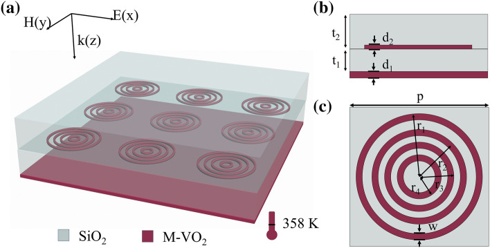
The simulation works are carried out using finite element method (FEM) with commercially available software COMSOL Multiphysics 5.5. A unit cell of the proposed absorber is simulated using periodic boundary condition along the in-plane x- and y- axes and perfectly matched layers along the propagation direction (z-axis). Inspired by the above discussions, here we propose an ultra-broadband THz MMA based on multi-ring metallic VO2 resonator array (MMVA), as shown in Fig. 1. Four 0.5 µm-thick concentric VO2 rings are imbedded in two dielectric layers, and 1 µm-thick VO2 continuous film is deposited at the bottom of the structure. Figure 1b, c exhibit the side view and top view of an unit cell. Due to the IMT phase-change feature of VO2, the MMVA layer exhibits the same behavior as metal resonators when the ambient temperature is above 358 K, and can strongly react with the incident wave, and generate an LSPR mode, which will couple with the bottom metallic VO2 film. On the other hand, at room temperature, VO2 behaves as a transparent dielectric material, resulting in a relatively weak interaction between the VO2 structure and incident light. Therefore, a temperature-switchable THz metasurface is achieved utilizing the IMT characteristics of VO2.
Figure 1.
(a) Schematic diagram of the ultra-broadband adjustable metamaterial absorbing structure based on VO2. Four-ring nested VO2 periodic array structure with thickness of 0.5 μm is embedded between two layers of SiO2. Bottom layer is 1 μm-thick VO2 film. At 358 K, VO2 transforms into metal state, and the structure exhibits THz broadband absorption characteristics. (b) Side-view and (c) top-view of unit cell. Geometric parameters are p = 90 μm, r1 = 42 μm, r2 = 34 μm, r3 = 25 μm, r4 = 19 μm, t1 = 22 μm, t2 = 39 μm, d1 = 1 μm, d2 = 0.5 μm, and w = 2 μm, respectively.
The dielectric permittivity of VO2 in THz range can be described by the Drude mode49,50 , where is the permittivity at high frequency, is the conductivity-dependent plasmon frequency, and stands for the collision frequency36,51. In addition, and are proportional to the free carrier density. At a specific conductivity, , the plasmon frequency can approximately be defined by , where , and . The conductivity of VO2 film in the fully insulating and the metallic states, which correspond to 298 K (room temperature) and 358 K, are assumed to be and , respectively43,47. SiO2 is modeled as lossless dielectric material with permittivity 52,53.The whole structure is considered to be placed on an infinite SiO2 substrate to avoid the Fabry–Perot resonance at room temperature.
Results and discussions
We performed finite element method (FEM) numerical simulations to investigate the proposed design. Firstly, we considered the high temperature (358 K) condition, where VO2 is at the metallic state. As shown in Fig. 2, we calculated the reflection, transmission, and absorption spectra of the proposed design at 358 K. It is clear that in this working mode, the transmission spectrum values (blue dotted line) from 0.3 to 1.5 THz are almost 0, which demonstrates that a 1 µm-thick metallic state VO2 (M-VO2) film can effectively cut off transmission in this frequency range. Furthermore, according to the reflection spectrum (green dotted line), such a M-VO2 configuration can effectively tune the impedance of the structure to match with the free space from 0.398 to 1.356 THz, thus leading to the reflectivity lower than 0.1 in this range. The absorption of the structure can be calculated as A(ω) = 1 − T(ω) − R(ω), and is shown in Fig. 2a (red solid line). Obviously, at 358 K the structure exhibits a highly efficient (above 90%) absorptivity ranging from 0.398 to 1.356 THz. At 0.83 THz, the absorptivity exceeds 99%, which is near perfect absorption. In particular, the calculated RAB, defined as , where and are the highest and lowest frequencies with absorptivity in excess of 90%, respectively, reaches about 109.2%.
Figure 2.
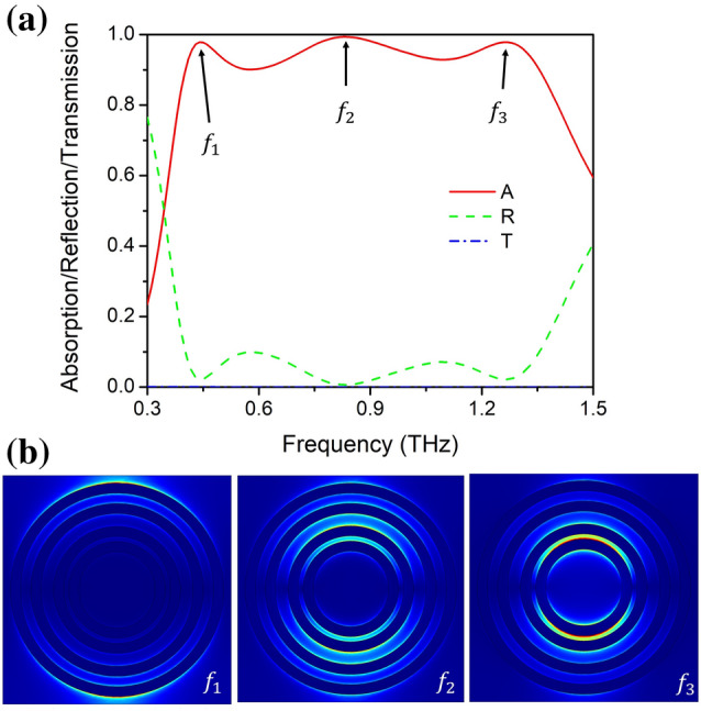
(a) Absorption spectra of ultra-broadband absorption structure at 358 K (VO2 conductivity of 200,000 S/m). Red solid line (A) represents absorption rate, green dotted line (R) represents reflectivity, and blue dotted line (T) stands for transmittance. (b) Distribution of electric field at three peak locations of ultra-broadband absorption spectrum.
It is worth noting that only three absorption peaks can be identified, even though we adopted four metallic VO2 ring array as resonators. This can be explained by the fact that the absorption peaks do not necessarily correspond to the resonances, especially in such a complex structure with a broadband absorption superposed by multiple resonance modes, one absorption peak can be a result of the superposition of multiple resonant absorption modes with small Q-values. In Fig. 2b we show the electric field distribution at the three absorption peaks. For simplicity, we denote the four rings from the largest to the smallest as r1–r4. It is clear that at f1 the electric field concentrates mainly at the edge of r1, and partly at the edge of r2, which means that the absorption peak at f1 can be attributed to the resonance of r1 and r2. Similarly, the absorption peak at f3 is generated by the resonance of r3 and r4. Moreover, at f2, the electric field concentrates at the edge of all the rings, which means that the absorption peak at f2 resulted from complex superposition and coupling effects of the four metallic VO2 rings.
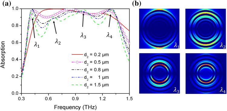
Due to the finite conductivity of metallic-state VO2, the electromagnetic responses of the absorber are sensitive to the thickness of MMVA. As shown in Fig. 3a, we calculated the absorption as a function of the thickness of MMVA d2. It can be seen that, at larger thickness, for example d2 = 1.5 µm, four absorption peaks can clearly be observed. Electric field distributions at the four absorption peaks in the MMVA layer are shown in Fig. 3b. Notably, the four absorption peaks correspond to the strong electric field concentration of rings with different radii. When d2 decreases, Q-factors of each absorption peaks decrease, resulting in an increase of the dips between absorption peaks, i.e., flattened the top. At the same time, the absorption bandwidth also decreases. When d2 = 0.5 µm, the dips between absorption peaks are increased to above 90%, and highly-efficient ultra-broadband absorption is achieved. When d2 decrease further to 0.2 μm, which is much smaller than the skin depth of metallic-state VO2 (about 1 µm at 1 THz) in this frequency range, the absorption bandwidth exhibits a significant decrease. This can be explained by that the decrease of d2 can lead to an increase of loss, thus weakening the resonance which further decreases the Q factor of the absorption spectrum generated by each ring resonator. The corresponding absorption factor Qa and radiative factor Qr are changed accordingly, resulting in significant change in the broadband absorption spectrum54.
Figure 3.
(a) Absorption spectra as a function of thickness of VO2 rings. (b) Electric field distributions at the four absorption peaks in the MMVA layer.
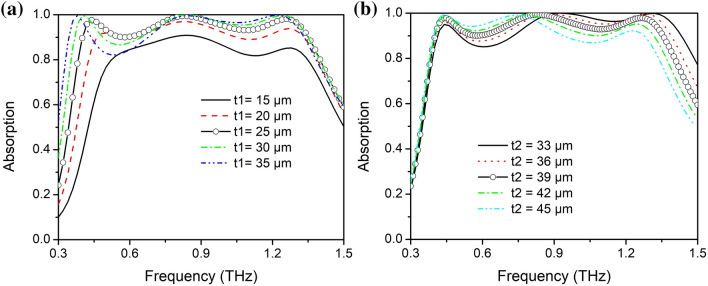
In order to improve the impedance matching and further optimize the broadband absorption performance, a layer of SiO2 is designed on top of the traditional MIM configuration, thus offering more freedom to shape the broadband absorption spectrum via tuning the thickness of two SiO2 layers. As shown in Fig. 4, the relationship between absorption spectra and the thickness of SiO2 layers t1 and t2 was analyzed. The thickness of lower SiO2 layer t1 can greatly influence the coupling effect between the MMVA and the bottom VO2 film, which can change the impedance condition and absorption performance of the structure obviously. As depicted in Fig. 4a, with an increase in t1, the absorptivity of the proposed structure exhibits an overall increase first, but when it reaches 100%, a part of the broadband absorption begins to decrease. This can be explained by the fact that with the increase in t1, each absorber based on a single VO2 ring will first exhibit an increase, and then a decrease, depending on the proximity to the impedance matching condition (IMC). Therefore, when t1 increases from 15 to 20 µm, the absorption corresponding to each ring increases due to approaching the IMC, and results in an overall increase of the superposed broadband absorption spectrum. When t1 increases gradually from 20 to 35 µm, part of the resonances increase beyond the critical point of IMC while the others not, which results in a decrease of the average absorptivity. As shown in Fig. 4b, with the increase of the upper SiO2 thickness t2, the absorptivity of higher frequency band decreases, while the lower frequency band increases. Due to the larger refractive index of SiO2 compared to vacuum, the THz waves reflected from the MIM structure can be reflected at the SiO2-air interface and enter into the MIM structure again to be repeatedly absorbed. The two SiO2 layers can also be considered as a resonant cavity that confines incident light with the Fabry–Perot resonance. The increase of cavity length will lead to red-shifting of the resonant wavelength, which will result in an increased absorptivity in the lower frequency range and a decrease in the higher frequency range, respectively.
Figure 4.
Absorption spectrum modification with thickness of SiO2 layers t1 (a) and t2 (b).
Notably, such a broadband absorption design based on concentric-ring resonator offers high scalability to control the absorption bandwidth by removing or cascading VO2 rings. Figure 5 shows the absorption spectra with the number of rings gradually increasing from the outside to the inside. When there is only one outer ring with r1 = 42 μm, the broadband absorption spectrum ranges from 0.38 to 0.77 THz with absorptivity in excess of 78.5%. When the second ring is added, the broadband absorption bandwidth increases to the range from 0.38 to 0.85 THz with absorptivity larger than 85%. The broadband absorptivity is relatively small, because the thicknesses of the two SiO2 layers t1 and t2 are optimized for four-ring ultra-broadband absorption, and for each single ring it may be over or under the IMC. By changing t1 and t2, broadband absorption absorptivity above 90% may also be achieved under this condition. Increasing the number of rings further, the absorption bandwidth also shows a clear increase. When there are three rings in the MMVA, the absorption bandwidth increases to the range from 0.398 to 1.125 THz (with the absorptivity in excess of 90%), the lower frequency range absorption is almost the same as that in the two ring-based absorbers, while in the higher frequency ranging from 0.84 to 0.99 THz, the absorptivity reaches up to 99.9%, with a near perfect absorption bandwidth of approximately 16.4%. When there are four periodic VO2 rings in MMVA layer, as discussed before, the absorption bandwidth increases further to 0.398~1.356 THz with the absorptivity above 90% and RAB of approximately 109.2%.
Figure 5.
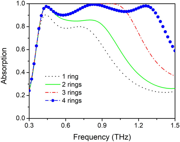
Absorption spectra with number of rings gradually increases from outside to inside.
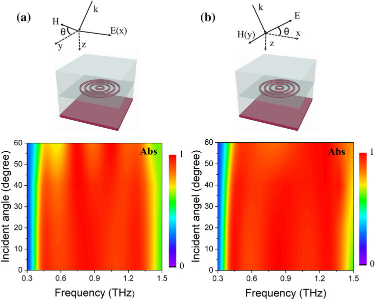
In most practical applications, there is a requirement that the broadband absorption spectrum be relatively insensitive to the incident angle. Thus, we calculated the performance of the structure for incident angles from 0 to 60° and different polarization states when VO2 is in the metallic phase. Figure 6 presents the absorption maps as a function of the incident angle in transverse-electric (TE) and transverse-magnetic (TM) polarization states (the electric/magnetic field remains parallel to the x/y axis, as shown in the Fig. 6). It is worth noting that under both polarization states the structure maintains absorptivity larger than 80%, when the incident angle is lower than 40°. If the incident angle is further increased from 40° to 60°, the TE state condition exhibits an obvious decrease in absorption around 0.6 THz, but absorptivity remains larger than 70% at the incident angle of 60°. The obvious decrease in absorptivity may be attributed to the reverse current generated in the metallic VO2 rings due to the increase of magnetic component. On the other hand, at the TM polarization state the absorptivity remains larger than 80%, even when the incident angle reaches 60°. Moreover, we calculated the absorption spectra with the fluctuations of material parameters and geometrical dimensions (see session 3 in supporting information), and demonstrated the structure with excellent tolerance for experiment errors.
Figure 6.
Absorption (Abs) spectra in (a) TE and (b) TM polarization states as function of incident angle.
When the ambient temperature drops to 298 K (room temperature), corresponding to the conductivity of VO2 of 200 S/m, VO2 is in the dielectric-phase with a high refractive index. We have calculated the transmission, reflection, and absorption spectra of the structure at a high temperature (358 K, VO2 conductivity of 200,000 S/m) and room temperature (VO2 conductivity of 200 S/m), and show them in Fig. 7. It is noted that the proposed structure exhibits two completely different functions at different ambient temperatures. At 358 K, the device works as an ultra-broadband absorber with RAB of approximately 109.2% and absorptivity in excess of 90%. However, at 298 K the structure shows high transmission of approximately 80%, and the absorptivity drops to about 7% at the same time. Thus, utilizing the IMT characteristics of VO2, a switchable multifunction THz metasurface is achieved, which can work as an ultra-broadband absorber and a highly-transparent material. Moreover, during the IMT process, there are many intermediate states of VO2 with different conductivities. As shown in the Fig. S1 of supporting information, we calculated the absorption, transmission, reflection spectra with the increasing of VO2 conductivity from 200 to 200 000 S/m, the absorptivity in the range of 0.398~1.356 THz increase from below 10% to above 90% gradually and the transmittance decrease from above 80% to near 0. Since the intermediate states of VO2 are dependent on the heating temperature, such a phenomenon can be used as a temperature sensor or thermally controllable multilevel ultra-broadband absorber.
Figure 7.
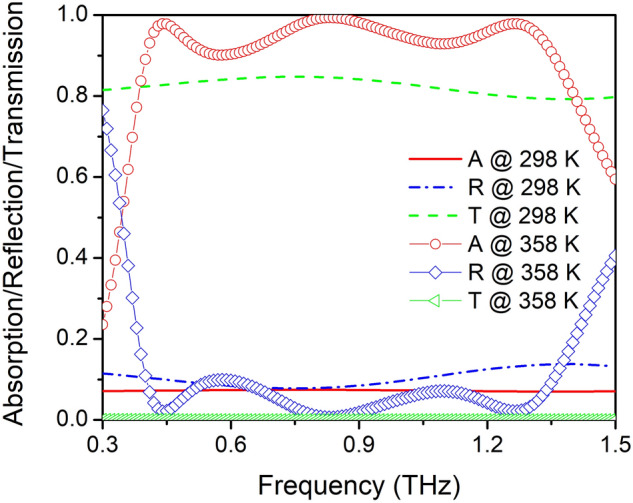
Transmission, reflection, and absorption spectra of structure at high temperature (358 K, VO2 conductivity of 200,000 S/m) and at room temperature (VO2 conductivity of 200 S/m). Red line (A) represents the absorption rate, blue line (R) represents the reflectivity, and green line (T) stand for the transmittance.
Conclusions
We have proposed a thermally switchable THz metasurface that exhibits two totally different work modes at room temperature and high temperature on the basis of the IMT characteristic of VO2. At 358 K, VO2 exhibits metallic-phase characteristics, and can strongly interact with the incident THz waves. By superposing the resonance-induced absorption of the metallic-phase VO2-ring based absorbers, an ultra-broadband absorption ranging from 0.398 to 1.356 THz with absorptivity in excess of 90% and the RAB reaches up to 109.2%. Electric field distribution at the absorption peaks shows that multiple hybrid plasmonic resonant modes collectively contribute to the observed ultra-broadband absorption. At 298 K, VO2 exhibits the characteristics of a transparent dielectric. In this case the interaction between the VO2 structure and incident waves is relatively weak, thus the structure is highly transparent (approximately 80% transmission). Herein, the proposed thermally switchable THz metasurface may have potential applications in various fields, such as optical switching, THz imaging, modulating and filtering.
Supplementary Information
Acknowledgements
National Natural Science Foundation of China (NSFC) (61875256, 61675219). Hongxing Dong acknowledges the Youth Top-notch Talent Support Program in Shanghai, Shanghai Rising-star Program, (2019CT001).
Author contributions
N.M. conceived the idea, performed the simulations, and wrote the initial draft. B.T. and J.L. assisted the revision of the manuscript, H.D. and L.Z. supervised the entire project.
Competing interests
The authors declare no competing interests.
Footnotes
Publisher's note
Springer Nature remains neutral with regard to jurisdictional claims in published maps and institutional affiliations.
Contributor Information
Hongxing Dong, Email: hongxingd@siom.ac.cn.
Long Zhang, Email: lzhang@siom.ac.cn.
Supplementary Information
The online version contains supplementary material available at 10.1038/s41598-022-04772-4.
References
- 1.Liu N, Mesch M, Weiss T, Hentschel M, Giessen H. Infrared perfect absorber and its application as plasmonic sensor. Nano Lett. 2010;10:2342–2348. doi: 10.1021/nl9041033. [DOI] [PubMed] [Google Scholar]
- 2.Liu X, et al. Taming the blackbody with infrared metamaterials as selective thermal emitters. Phys. Rev. Lett. 2011;107:045901. doi: 10.1103/PhysRevLett.107.045901. [DOI] [PubMed] [Google Scholar]
- 3.Watts CM, Liu X, Padilla WJ. Metamaterial electromagnetic wave absorbers. Adv. Mater. 2012;24:OP98–OP120. doi: 10.1002/adma.201200674. [DOI] [PubMed] [Google Scholar]
- 4.Atwater HA, Polman A. Plasmonics for improved photovoltaic devices. Nat. Mater. 2010;9:205–213. doi: 10.1038/nmat2629. [DOI] [PubMed] [Google Scholar]
- 5.Zhang K, Wang Y, Burokur SN, Wu Q. Generating dual-polarized vortex beam by detour phase: From phase gradient metasurfaces to metagratings. IEEE Trans. Microw. Theory Tech. 2021 doi: 10.1109/TMTT.2021.3075251. [DOI] [Google Scholar]
- 6.Zhang K, et al. Polarization-engineered noninterleaved metasurface for integer and fractional orbital angular momentum multiplexing. Laser Photon. Rev. 2021;15:2000351. [Google Scholar]
- 7.Shelby RA, Smith DR, Schultz S. Experimental verification of a negative index of refraction. Science. 2001;292:77–79. doi: 10.1126/science.1058847. [DOI] [PubMed] [Google Scholar]
- 8.Fang N. Sub-diffraction-limited optical imaging with a silver superlens. Science. 2005;308:534–537. doi: 10.1126/science.1108759. [DOI] [PubMed] [Google Scholar]
- 9.Li J, Pendry JB. Hiding under the carpet: A new strategy for cloaking. Phys. Rev. Lett. 2008;101:203901. doi: 10.1103/PhysRevLett.101.203901. [DOI] [PubMed] [Google Scholar]
- 10.Landy NI, Sajuyigbe S, Mock JJ, Smith DR, Padilla WJ. Perfect metamaterial absorber. Phys. Rev. Lett. 2008;100:207402. doi: 10.1103/PhysRevLett.100.207402. [DOI] [PubMed] [Google Scholar]
- 11.Tao H, et al. A metamaterial absorber for the terahertz regime: Design, fabrication and characterization. Opt. Express. 2008;16:7181–7188. doi: 10.1364/oe.16.007181. [DOI] [PubMed] [Google Scholar]
- 12.Shen, X. et al. Triple-band terahertz metamaterial absorber: Design, experiment, and physical interpretation. Appl. Phys. Lett.101, 154102 (2012).
- 13.Savo S, Shrekenhamer D, Padilla WJ. Liquid crystal metamaterial absorber spatial light modulator for THz applications. Adv. Opt. Mater. 2014;2:275–279. [Google Scholar]
- 14.Wang BX, et al. Theoretical investigation of broadband and wide-angle terahertz metamaterial absorber. IEEE Photonics Technol. Lett. 2014;26:111–114. [Google Scholar]
- 15.Fan R, Xiong B, Peng R, Wang M. Constructing metastructures with broadband electromagnetic functionality. Adv. Mater. 2019;32:1904646. doi: 10.1002/adma.201904646. [DOI] [PubMed] [Google Scholar]
- 16.He Q, Sun S, Zhou L. Tunable/reconfigurable metasurfaces: Physics and applications. Research. 2019;2019:1–16. doi: 10.34133/2019/1849272. [DOI] [PMC free article] [PubMed] [Google Scholar]
- 17.Yu P, et al. Broadband metamaterial absorbers. Adv. Opt. Mater. 2019;7:1800995. [Google Scholar]
- 18.Hao J, et al. High performance optical absorber based on a plasmonic metamaterial. Appl. Phys. Lett. 2010;96:251104. [Google Scholar]
- 19.Li Y, et al. A Tunable metasurface with switchable functionalities: From perfect transparency to perfect absorption. Adv. Opt. Mater. 2020;8:1901548. [Google Scholar]
- 20.Zhou J, Kaplan AF, Chen L, Guo LJ. Experiment and theory of the broadband absorption by a tapered hyperbolic metamaterial array. ACS Photonics. 2014;1:618–624. [Google Scholar]
- 21.Zhu J, et al. Ultra-broadband terahertz metamaterial absorber. Appl. Phys. Lett. 2014;105:21102. [Google Scholar]
- 22.Ding F, Cui Y, Ge X, Jin Y, He S. Ultra-broadband microwave metamaterial absorber. Appl. Phys. Lett. 2012;100:103506. [Google Scholar]
- 23.Aydin K, Ferry VE, Briggs RM, Atwater HA. Broadband polarization-independent resonant light absorption using ultrathin plasmonic super absorbers. Nat. Commun. 2011;2:517. doi: 10.1038/ncomms1528. [DOI] [PubMed] [Google Scholar]
- 24.Kenney M, et al. Octave-spanning broadband absorption of terahertz light using metasurface fractal-cross absorbers. ACS Photon. 2017;4:2604–2612. [Google Scholar]
- 25.Ji C, et al. Engineering light at the nanoscale: Structural color filters and broadband perfect absorbers. Adv. Opt. Mater. 2017;5:15–34. [Google Scholar]
- 26.Ding F, et al. Broadband near-infrared metamaterial absorbers utilizing highly lossy metals. Sci. Rep. 2016;6:39445. doi: 10.1038/srep39445. [DOI] [PMC free article] [PubMed] [Google Scholar]
- 27.Wang, W. et al. Broadband optical absorption based on single-sized metal-dielectric-metal plasmonic nanostructures with high- ε ″ metals. Appl. Phys. Lett.110, 101101 (2017).
- 28.Huang Y, et al. A refractory metamaterial absorber for ultra-broadband, omnidirectional and polarization-independent absorption in the UV-NIR spectrum. Nanoscale. 2018;10:8298–8303. doi: 10.1039/c8nr01728j. [DOI] [PubMed] [Google Scholar]
- 29.Thongrattanasiri, S., Koppens, F. H. L., Garcı, J. & Javier Garcıa de Abajo, F. Complete optical absorption in periodically patterned graphene. Phys. Rev. Lett.108, 047401 (2012). [DOI] [PubMed]
- 30.Feng H, et al. Tunable polarization-independent and angle-insensitive broadband terahertz absorber with graphene metamaterials. Opt. Express. 2021;29:7158–7167. doi: 10.1364/OE.418865. [DOI] [PubMed] [Google Scholar]
- 31.Mou N, et al. Hybridization-induced broadband terahertz wave absorption with graphene metasurfaces. Opt. Express. 2018;26:11728–11736. doi: 10.1364/OE.26.011728. [DOI] [PubMed] [Google Scholar]
- 32.Song S, Chen Q, Jin L, Sun F. Great light absorption enhancement in a graphene photodetector integrated with a metamaterial perfect absorber. Nanoscale. 2013;5:9615–9619. doi: 10.1039/c3nr03505k. [DOI] [PubMed] [Google Scholar]
- 33.Yao Y, et al. Electrically tunable metasurface perfect absorbers for ultrathin mid-infrared optical modulators. Nano Lett. 2014;14:6526–6532. doi: 10.1021/nl503104n. [DOI] [PubMed] [Google Scholar]
- 34.Lv T, et al. Switchable dual-band to broadband terahertz metamaterial absorber incorporating a VO2 phase transition. Opt. Express. 2021;29:5437–5447. doi: 10.1364/OE.418020. [DOI] [PubMed] [Google Scholar]
- 35.Sreekanth KV, Han S, Singh R. Ge2Sb2Te5-based tunable perfect absorber cavity with phase singularity at visible frequencies. Adv. Mater. 2018;30:1706696. doi: 10.1002/adma.201706696. [DOI] [PubMed] [Google Scholar]
- 36.Chen L, Song Z. Simultaneous realizations of absorber and transparent conducting metal in a single metamaterial. Opt. Express. 2020;28:6565–6571. doi: 10.1364/OE.388066. [DOI] [PubMed] [Google Scholar]
- 37.Dong W, et al. Tunable mid-infrared phase-change metasurface. Adv. Opt. Mater. 2018;6:1701346. [Google Scholar]
- 38.Lei L, et al. Tunable and scalable broadband metamaterial absorber involving VO2 -based phase transition. Photonics Res. 2019;7:734–741. [Google Scholar]
- 39.Qu Y, et al. Dynamic thermal emission control based on ultrathin plasmonic metamaterials including phase-changing material GST. Laser Photon. Rev. 2017;11:1700091. [Google Scholar]
- 40.Mou N, et al. Large-scale, low-cost, broadband and tunable perfect optical absorber based on phase-change material. Nanoscale. 2020;12:5374–5379. doi: 10.1039/c9nr07602f. [DOI] [PubMed] [Google Scholar]
- 41.Huang Y, et al. Multistate nonvolatile metamirrors with tunable optical chirality. ACS Appl. Mater. Interfaces. 2021;13:45890–45897. doi: 10.1021/acsami.1c14204. [DOI] [PubMed] [Google Scholar]
- 42.Liu M, et al. Switchable chiral mirrors. Adv Opt. Mater. 2020;8:2000247. [Google Scholar]
- 43.Song Z, Chen A, Zhang J, Wang J. Integrated metamaterial with functionalities of absorption and electromagnetically induced transparency. Opt. Express. 2019;27:25196–25204. doi: 10.1364/OE.27.025196. [DOI] [PubMed] [Google Scholar]
- 44.Liu H, et al. Switchable and dual-tunable multilayered terahertz absorber based on patterned graphene and vanadium dioxide. Micromachines. 2021;12:619. doi: 10.3390/mi12060619. [DOI] [PMC free article] [PubMed] [Google Scholar]
- 45.Liu H, Wang Z-H, Li L, Fan Y-X, Tao Z-Y. Vanadium dioxide-assisted broadband tunable terahertz metamaterial absorber. Sci. Rep. 2019;9:5751. doi: 10.1038/s41598-019-42293-9. [DOI] [PMC free article] [PubMed] [Google Scholar]
- 46.Wang S, et al. Vanadium dioxide based broadband THz metamaterial absorbers with high tunability: Simulation study. Opt. Express. 2019;27:19436–19447. doi: 10.1364/OE.27.019436. [DOI] [PubMed] [Google Scholar]
- 47.Ding F, Zhong S, Bozhevolnyi SI. Vanadium dioxide integrated metasurfaces with switchable functionalities at terahertz frequencies. Adv. Opt. Mater. 2018;6:1701204. [Google Scholar]
- 48.Prodan E. A Hybridization model for the plasmon response of complex nanostructures. Science. 2003;302:419–422. doi: 10.1126/science.1089171. [DOI] [PubMed] [Google Scholar]
- 49.Lv TT, et al. Hybrid metamaterial switching for manipulating chirality based on VO2 phase transition. Sci. Rep. 2016;6:23186. doi: 10.1038/srep23186. [DOI] [PMC free article] [PubMed] [Google Scholar]
- 50.Jepsen PU, et al. Metal-insulator phase transition in a VO2 thin film observed with terahertz spectroscopy. Phys. Rev. B. 2006;74:205103. [Google Scholar]
- 51.Liu M, et al. Terahertz-field-induced insulator-to-metal transition in vanadium dioxide metamaterial. Nature. 2012;487:345–348. doi: 10.1038/nature11231. [DOI] [PubMed] [Google Scholar]
- 52.Naftaly M, Miles RE. Terahertz time-domain spectroscopy of silicate glasses and the relationship to material properties. J. Appl. Phys. 2007;102:043517. [Google Scholar]
- 53.Song Z, et al. Terahertz absorber with reconfigurable bandwidth based on isotropic vanadium dioxide metasurfaces. IEEE Photonics J. 2019;11:4600607. [Google Scholar]
- 54.Qu C, et al. Tailor the functionalities of metasurfaces based on a complete phase diagram. Phys. Rev. Lett. 2015;115:235503. doi: 10.1103/PhysRevLett.115.235503. [DOI] [PubMed] [Google Scholar]
Associated Data
This section collects any data citations, data availability statements, or supplementary materials included in this article.


