Abstract
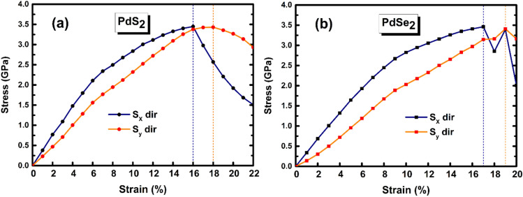
We studied the physical, electronic transport and optical properties of a unique pentagonal PdQ2 (Q = S, Se) monolayers. The dynamic stability of 2Dwrinkle like-PdQ2 is proven by positive phonon frequencies in the phonon dispersion curve. The optimized structural parameters of wrinkled pentagonal PdQ2 are in good agreement with the available experimental results. The ultimate tensile strength (UTHS) was calculated and found that, penta-PdS2 monolayer can withstand up to 16% (18%) strain along x (y) direction with 3.44 GPa (3.43 GPa). While, penta-PdSe2 monolayer can withstand up to 17% (19%) strain along x (y) dirrection with 3.46 GPa (3.40 GPa). It is found that, the penta-PdQ2 monolayers has the semiconducting behavior with indirect band gap of 0.94 and 1.26 eV for 2D-PdS2 and 2D-PdSe2, respectively. More interestingly, at room temperacture, the hole mobilty (electron mobility) obtained for 2D-PdS2 and PdSe2 are 67.43 (258.06) cm2 V−1 s−1 and 1518.81 (442.49) cm2 V−1 s−1, respectively. In addition, I-V characteristics of PdSe2 monolayer show strong negative differential conductance (NDC) region near the 3.57 V. The Shockly-Queisser (SQ) effeciency prameters of PdQ2 monolayers are also explored and the highest SQ efficeinciy obtained for PdS2 is 33.93% at −5% strain and for PdSe2 is 33.94% at −2% strain. The penta-PdQ2 exhibits high optical absorption intensity in the UV region, up to 4.04 × 10⁵ (for PdS2) and 5.28 × 10⁵ (for PdSe2), which is suitable for applications in optoelectronic devices. Thus, the ultrathin PdQ2 monolayers could be potential material for next-generation solar-cell applications and high performance nanodevices.
Subject terms: Two-dimensional materials, Electronic devices
Introduction
Atomically thin two-dimensional (2D) structures like, honeycomb lattice graphene1,2, boron nitride (BN)3,4, transition metal dichalcogenides (TMDs), group—IV, V5,6 elements has recived attention due to their potential applications in the field of electronics, optoelectronics, solar cell, energy harvesting, and biomedical technologies with the high possibilities of replacing traditional 2D materials1–7. Among the 2D materials, if targeting application in nanodevices, MX2 (M = Mo, W, V, Ti, Pd, Pt; X = S, Se, Te) type TMDs are technologically favourable materials7–9. Nowadays, an endless research is going on traditional TMDs layered materials, which is in demand of high mobility, high stability in air and strain modulated bandgap. Of these, many of TMDs has been already synthesized via the various method of exfoliation10–14. Interestingly, palladium based dichalcogenides has brought 2D with buckled or puckered pentagonal structures under the spotlight because of its unique lattice arrangement and fascinating properties such as fine tuning their physical, elctronic, thermal and optical properties.
Gronvold et al., studied the PdS2/PtS2 and concluded that noble metals (Pd and Pt) would be a layered structure with sulphur atoms15,16. Afterwards, in 2015 Wang et al., theoretically reported that 2D PdS2 is semiconductor with moderate indirect band gap up to ~ 1.60 eV, which is very significant in fabrication of nanodevices17. Moreover, Cheng et al.,18 have developed ultrafast Yb doped fiber laser using few layers of PdS2 and indicated that layered PdS2 can be a favourable candidate for photonics application. Some work have been reported on the layered PdSe2 via method of mechanical exfoliated, atomic-resolution scanning transmission electron microscopy (AR-STEM) and chemical vapor deposition (CVD)14,19–24. For Example, Akinola et al.,24 had fabricated few layers puckered pentagonal PdSe2 by AR-STEM method and demonstrated that, PdSe2 exhibits good ambipolar semiconducting nature with room temperature electron-apparent field-effect mobility (up to ~ 158 cm2 V−1 s−1) and its stability is remain same up to 60 days. It has been noted that having high mobility (electron/hole) and band gap between 1.2 ~ 1.9 eV of TMD, it makes them suitable for the FETs (field effect transistors) and CMOS applications, respectively25–28.
Recently, Weiting and their research group29 had successfully synthesized 2D PdSe2 nanosheets on 300 nm SiO2/Si substract and claimed that it is really promising material to make infrared photodetector due to its high-photoresponsivity (~ 660 A.W−1 under 914 nm laser) in harsh condition, which may be benefitted in military field for night-time detection because of its ability to work at night as well as in bad whether conditions. Beside these, few other reports theoretical are also available on the 2D pentagonal type PdQ2 monolayers17,30–34. Deng et al.,31 investigated the strain applied mechanical, electronic and optical properties of PdS2, PdP2 and PtSe2. Except this, none of works have been reported on strain applied mechanical, electronic, optical and electronic transport properties of 2D penta-PdQ2 (Q = S, Se). Further, the lower band gap of 2D-PdQ2 monolayers has also motivated us to investigate absorbance of solar radiation on nanosheet. Hence, we also studied the strain dependent solar cell power conversion efficiency % (PCE) of penta-PdQ2 (Q = S, Se) monolayers.
In this work, we have investigated the geometric, mechanical, electronic transport and optical properties of penta-PdQ2 using density functional theory (DFT). After the optimization of structures, we analysed the lattice parameters (Å), band gap (eV) and effective mass (m*). Then after we applied biaxial strain ɛ (%) and obtained its bulk modulus B (GPa). The ultimate tensile strength (UTHS) is also found under the tensile strain (+ ɛ%) for PdQ2 (Q = S, Se). We also studied the influence of loading on the band edges and obtained carrier mobility (µ2D) along biaxial strain ɛ (%). We have adopted Shockley-Queisser (SQ) method to study Solar cell efficiency η (%) and calculated the maximum power density (). The optical properties including the dielectric constants, absorption co-efficient, refractive index, and reflectivity of penta-PdQ2 (Q = S, Se) monolayers are also reported in this paper. Herein, "Computational methods" section contains the methedology of computations, "Results and discussion" section includes the results and disccusion part of the work on penta-PdQ2 (Q = S, Se) monolayers.
Computational methods
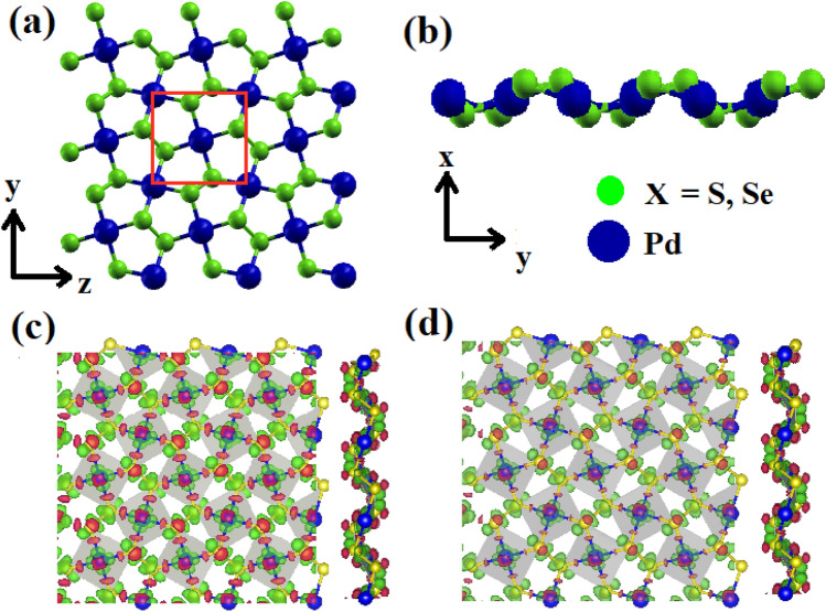
The structural, electronic transport and optical properties of 2D wrinkled PdQ2 (Q = S, Se) monolayers were performed with in the SIESTA code35. The exchange–correlation functional approach was used in term of Perdew–Burke-Ernzerhof (PBE) type pseudopotential36. The basic unit cell of 2D-PdQ2 (Q = S, Se) contains two Pd atoms and four Q (Q = S, Se) atoms as shown in Fig. 1. An energy cut-off of 450 and 300 Ry for PdS2 and PdSe2 monolayers were adopted, respectively. The doubled zeta plus (DZP) basis set was used with an energy of 0.02 Ry to expand the Kohn–Sham orbital. The Г- centred mesh of 20 × 20 × 1 and 15 × 15 × 1 k-points were sampled for PdS2 and PdSe2 monolayers, respectively under the Monkhorst–pack scheme in the 2D Brillouin zone37. The force 0.01 eV/Å was kept to relaxing the unstrained and strained structures of penta-PdQ2 (Q = S, Se) monolayers. The phonon dispersive curves were calculated using the density functional perturbation theory (DFPT) formalism38. In all calculation, the Fermi level (EF) is shifted at the zero energy. The parameters of carrier mobility of penta-PdQ2 (Q = S, Se) monolayers were found such as i.e., effective mass (m*), stiffness constants (C2D) and deformation energy (E1) approximations using the following formula proposed by the Bardeen and Shockley39, µ2D = ; here, e is elementary charge of an electron, ђ is the reduced Planck’s constant, C2D is the in-plane stiffness constant and for 2D system it is defined as = ; where S0 is cell area and a0 is the lattice constant at equilibrium, E and a are the total energy and lattice constant of the monolayer after deformation, is the Boltzmann constant, T is the temperature (300 K). Also, m* is the effective mass in the transport direction and E1 is the deformation potential (DP) constant denoting the shifting of each band edges due to the applied biaxial strain εxy defined as = ; where Eedge is energy value of VBM (for holes) and CBM (for electrons).
Figure 1.
(a) Top-view of penta-PdQ2 (Q = S, Se) monolayer structure. Red line indicats the unitcell of the system. (b) Side views from z- direction of the atomic structure of penta-PdQ2. The navy blue and light-green circles represent the Pd and Q (S, Se) atoms, respectively. The deformation charge density plot (c) for penta-PdS2 (d) for penta-PdSe2; where red and green colour indicate the charge accumulation (electron excess) and charge deplation (electron loss). The iso-level is 0.063 e/Å3 for both monolayers.
The electronic transport properties of PdQ2 monolayers are calculated by utilizing the non-equilibrium Green’s function (NEGF) in the form of I-V response by TRANSIESTA module of SIESTA code40,41. The electric current through the scattering region is calculated by exploring the Landauer-Buttiker formalism,
| 1 |
where T (E, Vbias) is the transmission probability of an electron incident at an energy E through the device under the bias voltage Vbias, and are the electrostatic potentials of left and right electrodes at a particular voltage bias and G0 is the unit of quantum conductance. The optical properties were investigated including the dielectric function and absorbance coefficient by DFT within the random phase approximation (RPA)42. The dielectric function is given by ɛ (ω) = ɛ’ (ω) + i ε’’ (ω). Here, ε’(ω) and ε’’(ω) are the real and imaginary parts of the complex dielectric function43, respectively.
Results and discussion
Stability and mechanical properties
First, the geometric structures of pristine 2D penta-PdQ2 (Q = S, Se) were systemitically relaxed and lattice structures of penta- PdQ2 were obtained. It is built up with two Pd and four Q (S, Se) atoms in the unitcell as shown in Fig. 1a,b. The differential charge density in Fig. 1c,d shows an accumulation and depletion of charges between Pd and Q (S, Se) atoms. In Table 1, the relaxed structural parameters are summarized with ground state properties such as, lattice parameter (Å), distance d (Å) between Pd-Q1, Pd-Q2 and Q1-Q2, thickness t (Å) and cohesive energy Ecoh (eV/atom) of PdQ2 monolayers.
Table 1.
The calculated lattice parameter (Å), bond lengths d (Å), thickness t (Å) and cohesive energy Ecoh (eV/atom) of penta-PdQ2 monolayers.
| Penta-PdQ2 (Q = S, Se) | dPd-Q1 (Å) | dPd-Q2 (Å) | dX1-Q2 (Å) | Thickness (Å) | Lattice parameter (Å) | Cohesive energy Ecoh (eV/atom) | |
|---|---|---|---|---|---|---|---|
| Penta-PdS2 | Present work | 2.35 | 2.34 | 2.14 | 1.29 | a = 5.62, b = 5.42 | −4.71 |
| Other DFT/ *Exp | 2.3417 2.3532 | 2.3517 2.3432 | 2.1017 2.1132 | 1.2832 | a = 5.49, b = 5.5917 a = 5.48, b = 5.5932 a = 5.48, b = 5.5733 | – | |
| Penta- PdSe2 | present work | 2.45 | 2.45 | 2.42 | 1.47 | a = 5.94, b = 5.68 | −4.30 |
| Other DFT/ *Exp | 2.4534 | 2.4634 | 2.4234 | – | a = 5.72, b = 5.8029 * a = 5.74, b = 5.9132 a = 5.75, b = 5.9233 a = 5.71, b = 5.9034 | – |
As shown, in Table 1, the obtained lattice parameters a (b) of PdS2 and PdSe2 monolayers are 5.62 (5.42) Å and 5.94 (5.68) Å, respectively. The atomic distance between Pd-S1(Se1), Pd-S2(Se2), and S1(Se1)-S2(Se2) atoms are 2.35 (2.45) Å, 2.34 (2.42) Å and 2.14 (2.42) Å, respectively and shows good agreement with previously reported results17,29,32–34. To evaluate stability of resulted structures, the cohesive energy is calculated using the formula: Ecoh = Σ nX EX—EPdQ2/N. where EPdQ2 denotes total energy of PdQ2 (Q = S, Se) unit cell, N is total atom in unit cell and nX and EX are number of atoms of each element and atomic energies of each atom in the unit cell, respectively. It is found that cohesive energies for PdS2 and PdSe2 monolayer are −4.70 and −4.30 eV/atom, respectively. Although this is larger than that for the 2D-antimony (−4.03), 2D-arsenene (−2.96), 2D-MoS2 (−4.11), 2D-MoSe2 (−3.94) and 2D-black phosphorous (−3.48). This is evidence that penta-PdQ2 monolayers have strong bonding in its ring-network. In addition, to confirm the kinetic stability of penta-PdQ2 (Q = S, Se) structures, we calculated the phonon dispersion curves along high symmetric points for both PdS2 and PdSe2 monolayers and results are as shown in Figure S1 (a, b), ESI†. The highest phonon frequencies extended is up to 2275 cm-1 and 2193 cm-1 for PdS2 and PdSe2 monolayers, respectively. Evidently, no negative acoustics branch is appeared in the first Brillouin zone, itself proves the dynamical stability of both the monolayers at room temperature.
Next, we focused on mechanical properties of penta-PdQ2 and evaluated Young’s modulus Y (N/m) and bulk modulus B (N/m). The Young’s moduli Y (N/m) and bulk moduli B (N/m) were investigated under uniaxial and biaxial strain on the penta-PdQ2 monolayers. The range of applied strain is taken in interval of −5 +5 in the step of 1%. The bulk modulus computed by applying biaxial load (x and y) on the penta-PdQ2 monolayer with following relation44,45,
| 2 |
where S0 is unstrained cross-sectional area of the unit cell. Es and A are the total strain energy and area of respected applied strain, respectively. Figure S2 (a, b), ESI† shows the strain energy vs area curve for pristine and loaded structures of PdS2 and PdSe2 monolayers, respectively. This curve is fitted by the polynomial curve fitting and with help of Eq. (1), we have obtained bulk modulus B (N/m) as shown in Figure S2a,b, ESI†. The calculated bulk modulus (N/m) of PdS2 and PdSe2 are 30.22 and 23.56 N/m, respectively. These values are larger than that for the monolayer of Sb (~ 21.88 N/m) and As (~ 25.78 N/m)44,46, that indicate that penta-PdQ2 has stiffer and better resistance to deformation compared to antimony (Sb) and arsenene (As) monolayers. Afterwards, we have calculated the in-plane Young’s modulus Y (N/m) in longitudinal (along x-axis) or transverse (along y-axis) direction for penta-PdQ2. To obtained Young’s modulus from first-principles calculation, the following formula was employed44,45,
| 3 |
Here, S0 is unstrained cross-sectional area of the unicell. Next, shows the second derivative of strain energy (eV) with applied load. Here, the compressive and tensile strains are applied to the penta-PdQ2 in the longitudinal or transverse direction. The Young’s moduli obtained by using the curves shown in Figure S3a,b, ESI†. The calculated Young’s modulus Y (N/m) along x (y) direction are 74.13 (42.40) N/m and 65.26 (28.62) N/m for penta-PdS2 and penta-PdSe2, respectively. The results indicating that, Young’s modulus decreases as we switched S to Se, and this is due to the increment in the Pd-S and Pd–Se bond strength. Xiong et al.47 had calculated orientation-dependent Young’s modulus of 2D orthorhombic MX2 (M = Ni, Pd; X = S, Se, Te) and reported values are ~ 50 (37) N/m for PdS2 (PdSe2). From the present investigation of Young’s modulus of penta-PdQ2, we suggest that the 2D penta-PdQ2 can be preferred candidates for flexible devices because of having ultra-low values of Young’s modulus, compared to that of 2D graphene (340 N/m) and 2D MoS2 (125 N/m)48,49.
Further, we have also explored the mechanical stability of penta-PdQ2 monolayers and examined that up to which values of strain () the monolayers can withstand? It is worth to find curve of stress–strain relation called ultimate tensile strength (UTSH) curve50. The UTSH is representing the maximum stress value (GPa) that a monolayer can withstand prior to the fractured structure set. This can be calculated by the components of stress tensor with respect applied strain. The computed UTSH for penta-PdQ2 monolayers are shown in Fig. 2a,b. The stress value, where the slope of the stress–strain curve becomes zero indicates the value of UTSH, and the strain at this value represents the magnitude of ultimate tensile strain (UTSR). In case of penta-PdS2, the calculated values of UTSR along x (y) directions is 16 (18) at stress of 3.44 GPa and 3.43 GPa, respectively (see Fig. 2a). Whereas, in penta-PdSe2 (see Fig. 2b) it is observed at 17 (19) with stress value of 3.46 GPa (3.40) GPa. The present values of UTSR for penta-PdQ2 are higher than the blue-phosphorene monolayer (~ 16)51. Thus, the UTSR values suggest that the penta-PdQ2 monolayer is relatively more flexible.
Figure 2.
The stress (GPa) vs strain () curve under tensile strain. (a) For penta-PdS2 and (b) For penta- PdSe2.
Electronic properties
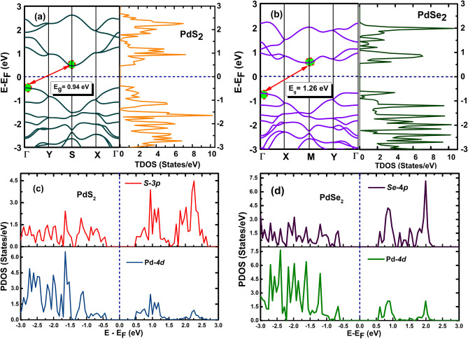
The band structure, total density of states (TDOS) and partial density of states (PDOS) of penta-PdQ2 monolayers along high symmetry points of Brillouin zone (BZ) have also investigated. At PBE level, from Fig. 3a,b we can see that the penta-PdS2 (PdSe2) is an indirect band gap with valence band maximum (VBM) and conduction band minimum (CBM) tracing at S- point (M-point) and Γ-point, respectively. The obtained indirect band gap of penta-PdS2 is EgPBE = 0.94 eV, while band gap for penta-PdSe2 is EgPBE = 1.26 eV as seen in Fig. 3a,b, both the values are consistent with previously reported results30,31. As DFT-PBE functional may underestimate the bandgaps of semiconductors, we also used GGA + U, LDA, LDA + U and HSE0652 approximations to ensure calculation reliability and the obtained indirect electronic bandgap of PdS2 (PdSe2) are 1.05 (1.26) eV, 0.92 (1.31) eV, 0.94 (1.30) and 0.92 eV, respectively. For the present computations, the Hubbard parameter value taken as 3.69 eV53. Next, having heavier element (Pd) in 2D penta-PdQ2 material, the spin–orbit coupling (SOC) effect may play a crucial role and could influence in the band gap (Eg) of material. Thus, we have also checked the SOC effect on the penta-PdQ2 monolayer and results are shown in Figure S4a,b, ESI†. Using PBE + SOC functional calculation, the obtained indirect band gap of penta-PdS2 is EgPBE+SOC = 1.16 eV, whereas band gap of penta-PdSe2 is EgPBE+SOC = 1.51 eV. Recently, the Yang et al.32, have reported electronic properties of penta-PdS2 from PBE (PBE + SOC) calculation and reported indirect band gap of 1.08 eV (1.13 eV), which is comparable with our results within of 12.96 (11.5) deviation. Moreover, a research group of Sun et al.34, have reported a band gap of penta-PdSe2 with PBE level theory and mentioned indirect band gap of 1.38 eV, which is higher by 8.6 than our obtained band gap (~ 1.26 eV). Furthermore, with SOC effect, Qin et al.33, has computed indirect band gap of penta-PdSe2 monolayer via TB-mBJ-GGA potential and reported band gap 1.38 eV. The deviation of present band gap of penta-PdSe2 with PBE + SOC calculation is 9. Further, the VBM and CBM are substantially coincide with each other regardless of PBE or HSE06 (with or without SOC) level calculations. Also, the HSE06 level calculations are really time expensive and need heavy computing power, as a results of that, we only used PBE functional level band structures for further calculations by applying strain. The nature of CBM and VBM are vary with applying strain on the PdQ2 monolayer to reach up the optimal value of 1.3 eV for solar cell applications, which is discussed in SQ Efficiency section. As presented in Fig. 3a,b, it is noticed that the TDOS (States/eV) are mostly ascend due to ‘d’ orbitals of Pd atom and ‘p’ orbitals of Q (S, Se) atom in the penta-PdQ2 monolayer, which are also consistent to the past reported results32,34. Additionally, the TDOS difference from PBE to PBE + SOC calculations are shown in Figure S5a,b, (ESI†) for PdS2 and PdSe2 monolayers. we have also investigated PDOS (States/eV) as displayed in Fig. 3 (c, d), to further investigate partial contribution of atoms in penta-PdQ2 and we conclude that the conduction bands (CBs) and valence bands (VBs) are highly occupied by the 4d-Pd states and 3p-Q (Q = S, Se) states, respectively.
Figure 3.
Electronic band structure and total density of states (TDOS) States/eV (a) For penta-PdS2 monolayer and (b) For penta-PdSe2 monolayer. The partial density of states (PDOS) States/eV (c) For penta-PdS2 monolayer and (d) For penta-PdSe2 monolayer.
Transport properties
Carrier mobility
We further focused on the band alignment in terms of strain effect to drive the electronic properties. Simultaneously, we have also calculated carrier mobility (µ) of monolayer, which is one of essential factor for a high-performance device like FET. For this, we have exerted compressive (-) and tensile (+ ) strain on penta-PdQ2 (Q = S, Se) monolayers and traced influence on the band edges of CBM and VBM in the band structure, where system is anisotropic (a not equal to b). The strength of strain along biaxial direction is given by54, = [(S−S0)/S0]100; here, S0 is the unstrained lattice constant and S is the strained lattice constant of the monolayer. The response of applied strain to band gaps of penta-PdQ2 is shown in Fig. 4.
Figure 4.
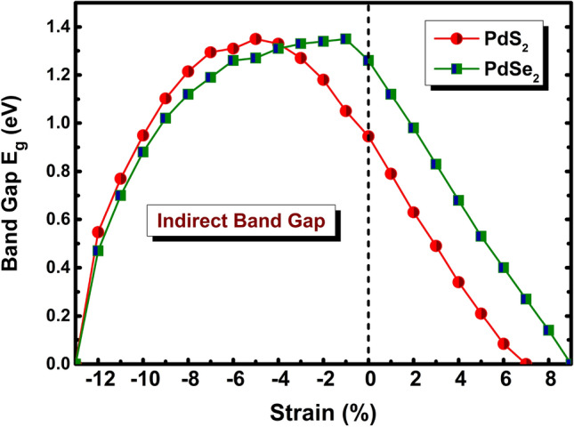
The variation of band gap Eg (eV) with applied biaxial strain () on penta-PdQ2 monolayers.
As stated before, the fundamental indirect band gap of penta-PdS2 and penta-PdSe2 is 0.96 eV and 1.26 eV, respectively. The Fig. 4 reflects that the band gap of penta-PdQ2 is gradually decreases almost linearly in presence of tensile strain (+ ) compared to fundamental band gap (0). Interestingly, upon increases compressive strain (−) band gap of penta-PdS2 increases up to -5 compressive strain and then decreases gradually with respect to 0. It is noteworthy that, the maximum value of band gap of penta-PdS2 is ~ 1.35 eV at = −5 and for penta-PdSe2 is ~ 1.36 eV at = −1 . Remarkably, the resistive phase transition is seen at higher compressive (−) and tensile strain (+ ) in both cases. The semiconducting nature of penta-PdS2 (PdSe2) is transform into semi-metallic (~ 0 eV) by applying the biaxial compressive and tensile strain of −13 (−13) and + 7 (+ 9), respectively. Under the critical compressive strain (−), the resistive phase change (semiconductor to semi-metallic) in penta-PdQ2 behaviour arises due to crossing one band of VBM at the Fermi level (Fig. S6a,b), ESI†). In contrary, up on the critical tensile (+ ) strain, it occurred due to touching one band of CBM at the Fermi level (Fig. S7a,b, ESI†). Additionally, we have also examined the phonon spectrum for each applied strain on penta-PdQ2 and computed its phonon frequency as summarized in Table S1, ESI†. Thus, our outcomes accomplish those electronic properties of studied 2D penta-PdQ2 (Q = S, Se) materials are tuneable by applying biaxial strain, which establish that the penta-PdQ2 is a promising candidate for designing flexible nanodevices.
Owing to tunability of penta-PdQ2 monolayers, we inspired to calculate the carrier mobility of penta-PdQ2 monolayers. For that the Bardeen and Shockley formalism39 had been applied, we have calculated the effective mass (m*), deformation potential E1 (eV) and stiffness constant C2D (J m-2) to check the flow of charge carrier along biaxial strain. The carrier mobility depends on the most influenced factor on the carrier effective mass m* of electron (e) and hole (h), that is directly derived from the electronic band structure as55,
| 4 |
Next, deformation potential E1 is another vital parameter to effect carrier mobility and is obtained from the deformation theory (DP)39, which has been also successfully used method in previous reports for 2D MoS2, WS2 and phosphorene. The needed ingredients for carrier mobility (µ) are summarized in Table 2. Along biaxial strain, the obtained effective mass (m*) of electron and hole for penta-PdS2 (PdSe2) are 0.39 me (0.58 me) and 0.72 me (0.14 me), respectively. Our computed deformation potential E1 (eV) for penta-PdS2 is −6.44 eV for e and 6.84 eV for h, that is consistent with ones reported by Wang et al.17, along x or y direction. While in case of penta-PdSe2, the value of E1 is −2.91 eV for e and 6.14 eV for h that is also in accordance with the results of Qin et al.,33 for x or y direction. Whereas the in-plane stiffness constant C2D for penta-PdQ2 has anisotropic behaviour. The in-plane stiffness constant obtained for penta-PdS2 and penta-PdSe2 are 121.76 J m-2 and 94.62 J m-2, respectively. The stiffness constant C2D of penta-PdS2 is larger than the penta-PdSe2, indicating that PdSe2 monolayer is softer than the penta-PdS2 monolayer. As shown in Table 2, the achieved electron mobility of penta-PdS2 monolayer is 258 cm2 V−1 s−1, which is quite higher than the hole mobility ~ 67 cm2 V−1 s−1. Also, the carrier mobility ratio R comes out to be 0.26. Moreover, Wang et al.17 has reported the electron mobilities (cm2 V−1 s−1) of penta-PdS2 as 40.97 (x) and 169.11 (y), while hole mobilities (cm2 V−1 s−1) as 339.25 (x) and 91.73 (y). On other hand, if we compare carrier transport along biaxial strain of penta-PdSe2 the hole mobility is 1518 cm2 V−1 s−1 that is greater than the electron mobility ~ 442.49 cm2 V−1 s−1 and R is 3.43. However, it is observed that the hole mobility of penta-PdSe2 is higher than the 2D phosphorene56 (i.e., 640–700 cm2 V−1 s−1) and BN nanosheet (i.e., 500 cm2 V−1 s−1)57, indicating that penta-PdSe2 would be a promising material for modelling electronic applications.
Table 2.
The carrier effective mass |m*| (me, the mass of free electrons), deformation potential constant E1 (eV), stiffness constant C2D (J m−2), carrier mobility (μ) for electron (e) and hole (h) and carrier mobility ratio (R) along biaxial direction of penta-PdQ2 monolayers at 300 K.
| System | Carrier type | m*/me | E1 (eV) | C2D (J m−2) | μ (cm2 v−1 s−1) | R = μh/μe |
|---|---|---|---|---|---|---|
| Penta-PdS2 | electron | 0.39 | −6.44 | 121.76 | 258.06 | 0.26 |
| hole | 0.72 | 6.85 | 121.76 | 67.43 | ||
| Penta-PdSe2 | electron | 0.58 | −2.91 | 94.62 | 442.49 | 3.43 |
| hole | 0.14 | 6.14 | 94.62 | 1518 |
Current–voltage (I-V) characteristics
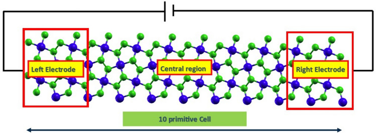
To understand the current sensitivity of the penta-PdQ2 monolayers, we have examined the I-V characteristics, based on the equivalent transport theory41. Figure 5 represents the schematic view of two-terminal device, where we have considered LE (left electrode), RE (right electrode) and scattering region of same material.
Figure 5.
Schematic view of two-terminal device of penta-PdQ2 monolayer. Here electrons are driven from the cold to the hot lead through central region.
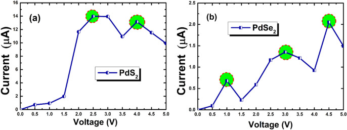
Here, we have taken 10 primitive cells, among them the lead had built up with four-unit cell (24 atoms) and central region consist of 12-unit cells (72 atoms). The I-V characteristic of both penta-PdS2 and penta-PdSe2 monolayers are shown in Fig. 6a,b. It is seen that, no significant current is observed till ~ 1.0 V and 1.5 V then it starts to increase with increasing applied voltages due to semiconducting nature of penta-PdS2 and PdSe2 monolayers, respectively. Apparently, it can be seen form Fig. 6a,b penta-PdS2 is more current-sensitive than the penta-PdSe2 monolayer. Although, in the case of penta-PdS2, the first peak in current is seen at 2.5 V with 14 µA and second current peak is located at 4.0 V with current of 13.2 µA. This is indicating a pronounced negative differential conductance effect (NDC)58 in the bias range 2.0–3.5 V (see Fig. 6a). While in case of penta-PdSe2, the NDC effect is seen in range of 1.0–4.5 V (see Fig. 6b). More precisely, the first NDC effect is occurs at the bias voltage 1.0 V and current to be found about 0.678 µA. Further, the second and third peaks are occurring at the bias voltage of 3.0 V and 4.5 V with current up to 1.35 µA and 2.05 µA, respectively. The NDC effect is very useful feature in I-V curve because it would be playing a crucial role in the application of multipliers, mixers, logic gates, high-frequency oscillators, and A to D (analog-to-digital) converters59.
Figure 6.
Current–voltage (I-V) plot of penta-PdQ2 under bias voltages from 0.0 V to 5.0 V. The negative differential conductance (NDC) regions are indicated by the highlighted circles.
SQ efficiency
We also focused on the power conversion efficiency (PCE) of penta-PdQ2 (Q = S, Se) using Shokley-Queisser (SQ) limit that gives the percentage of power converted to electrical energy60,61. For this we required several parameters such as short circuit current density (), open circuit voltage (), maximum power density () and efficiency . The theoretical short circuit current density is calculated using following relation62,63,
| 5 |
where is the elementary charge, represents the absorbance of layer62 and is the photon flux density as specified in the AM1.5G spectrum64, Also, the theoretical reverse saturation current is defined as 65; Here is the black body spectrum and the radiative recombination fraction, which is supposed to be unity60. Thus, the total current density can be obtained using the formula65,
| 6 |
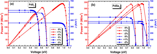
where is the Boltzmann’s constant, is the voltage over the absorber of the 2D devices. By the relation of , the maximum power density can be evaluated from the maxima of the curve, as presented in Fig. 7a,b. Eventually, with help of above-mentioned parameters, now we have obtained solar cell efficiency by formula59,
| 7 |
where is total incident power density from solar irradiation of AM1.5G and is maximum power density.
Figure 7.
The calculated characteristic and power density curves of (a) for penta- PdS2 and (b) for penta-PdSe2 for pristine and compressive (-) or tensile (+ )) loaded strain (maximum efficiency () of strain taken) at T = 300 K. .
As mentioned in the SQ limit theory, the electronic band gap (Eg) plays a pivotal role in the calculation of the material efficiency. Moreover, the maximum possible SQ efficiency limit is specified of 33.70 in circumstance of semiconductor with 1.34 eV optimum band gap66. As seen from the Table 3, the remarkable conversion efficiency for pristine penta-PdS2 and penta-PdSe2 is observed and are 30.79 and 33.54, respectively. Also, the efficiency of penta-PdSe2 is larger than the efficiency of benchmark GaAs (~ 31.4) solar cell with single junction. Next, the band gap of both monolayers could be well tuned from 0.34 eV ~ 1.35 eV under influence of biaxial strain () as shown in Fig. 8a,b. Therefore, we have also checked the conversion efficiency under compressive (−) and tensile strain (+ ) for both the monolayers and presented in Fig. 8a,b. It is noted that, when we have exerted compressive strain (−) on the penta-PdQ2 the efficiency at certain strain is higher as compared to the pristine (0 ), that of 33.93 (at −5 of penta-PdS2) and −33.94 (at −2 of penta-PdSe2). On other hand, under tensile strain the maximum efficiency arises that of 25.72 at + 1 of penta-PdS2 and 33.63 at + 1 of penta-PdSe2, which is lower than with respective each of pristine (0 ). This suggests that, by applying biaxial strain on the penta-PdQ2 the related SQ efficiency could be tuned. Also, the fabrications of penta-PdQ2 solar cell have potential to improve photovoltaic performance compared to traditionally use Si-based solar cells.
Table 3.
The calculated values of (A/m2), (W/m2) and of penta-PdQ2 (Q = S, Se) for both pristine and loaded strain (). Significant values are in bold.
| 2D-System | Strain () | (A/m2) | (W/m2) | Efficiency |
|---|---|---|---|---|
| Penta-PdS2 | 0% | 524.67 | 307.96 | 30.79% |
| + 1% | 555.79 | 257.2 | 25.72% | |
| −5% | 358.48 | 339.3 | 33.93% | |
| Penta-PdSe2 | 0% | 383.82 | 335.4 | 33.54% |
| + 1% | 449.66 | 336.3 | 33.63% | |
| −2% | 358.48 | 339.48 | 33.94% |
Figure 8.
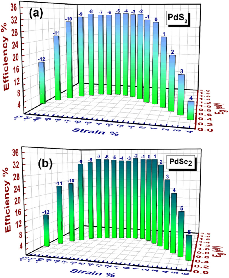
Change in SQ Efficiency η () of penta-PdQ2 monolayers for pristine and loaded strain at T = 300 K (a) For penta-PdS2 and (b) For penta-PdSe2.
Optical properties
In order to evaluate light absorption ability of penta-PdQ2, we have calculated the real (’) and imaginary (”) dielectric functions, absorption coefficient , refractive index , and reflectivity of penta-PdQ2 monolayers with parallel (E c) and perpendicular (E c) electric vector (E). The computation is carried out using the Kramers-Kroning (KK) relationship67 and results are shown in Figs. 9, S8 and S9, ESI†.
Figure 9.
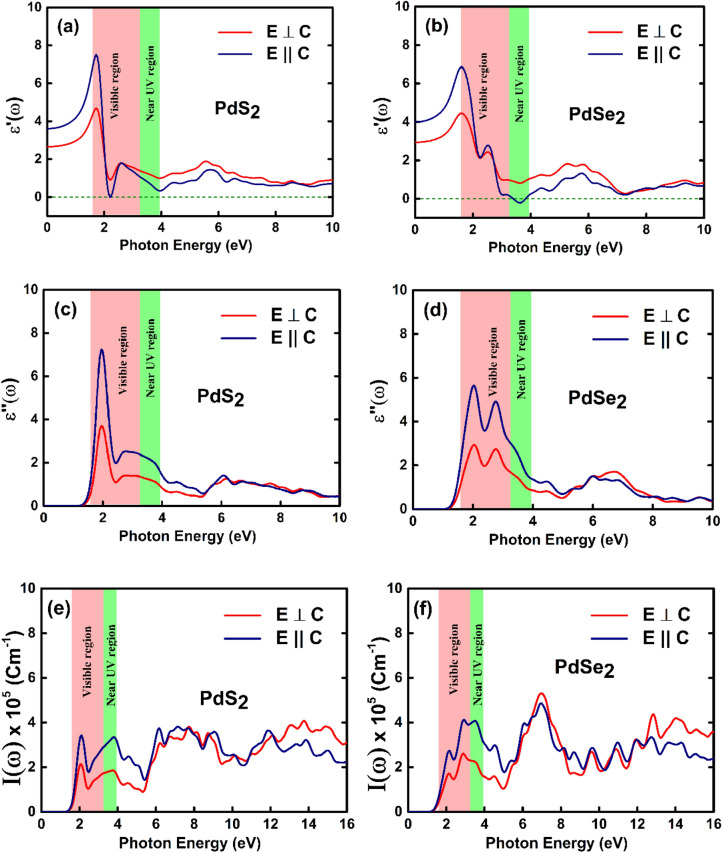
Computed optical properties of penta-PdQ2 monolayers for parallel and perpendicular polarization (a,b) real (’) and (c,d) imaginary (”) parts of complex dielectric function. (e,f) absorption coefficient .
In present work, the computed dielectric constants are shown in the large range of photon energy (ħω) from 0 to 10 eV and absorption coefficients in 0 to 16 eV. The visible (VIS; 1.59 – 3.26 eV) and near UV (UV-A; 3.26—3.94 eV) spectrum regions are shaded by the light-pink and light-green colour, respectively. Figure 9a,b shows the graphical image of real (’) and imaginary (”) components of penta-PdQ2, that simply gives the idea about the electronic polarizability of the material from the Clausis—Mossotti 68 relation. It can be seen from the Fig. 9a,b, the static dielectric constant ((0), (0)) of penta-PdS2 is (3.56, 2.62), while static dielectric constant of penta-PdSe2 is 4.0 ((0)) and 2.94 ((0)). This means that its (0) of parallel optical vector have more dominant polarizability compared to the perpendicular of (0). The optical peculiarity is strongly connected to the imaginary part of the dielectric function ”(ω), which reflects the transition between the energy bands near the EF levels and that would be govern the linear response of the material to light under small wave vector as depicted in Fig. 9 (c, d). Therefore, the imaginary part ”(ω) in case of penta-PdS2, the one major peak occurred at 1.98 eV in the visible (VIS) region for both and case as plotted in Fig. 9c. While, in case of penta-PdSe2, it is clearly seen (Fig. 9d) that there are two intense peaks appeared in the visible region (VIS) at ħω = 2.04 eV and 2.76 eV due to the electronic transition of ‘4p’ states of Se atom and ‘4d’ states of Pd atom between conduction bands (CBs) and valence bands (VBs) of the electronic band structure. Apparently, the peaks tendency of and are similar on the photon energy spectrum for both penta-PdQ2 monolayers.
The optical absorption spectra of the penta-PdQ2 were recorded by absorption coefficient vs photon energy (eV) as shown in Fig. 9e,f. For penta-PdQ2, the first absorption peak orientation is in the ~ 1.5–5 eV and second broad peak’s orientation is cover the UV region up to photon energy of 16 eV. For penta-PdS2, the low energy excitonic peak occur around 2.1 eV in infrared region (IR) and that peak rise towards the visible region at 3.78 eV for both the polarization. The maximum absorption coefficient of penta-PdS2 for parallel and perpendicular polarization is 3.65 × 10⁵ and 4.04 × 10⁵, respectively (See Fig. 9e). While, in case of penta-PdSe2, the first peak is located at 2.2 eV in the IR region and kick off in visible region at highest absorption coefficient of 4.12 105. However, with perpendicular polarization the highest coefficient found is about 5.28 105 in the UV region (See Fig. 9f). Thus, the penta-PdQ2 monolayers have shown prominent absorption in VIS and UV region, which suggest a good prospect of penta-PdQ2 monolayers as UV filters and UV photodetectors.
Next, the computed refractive index and reflectance of penta-PdQ2 have the same evolution curve as plotted in Figure S8 (a, b), ESI† and S9 (a, b), ESI†. In penta-PdS2, we observed static refractive index as ((0), (0)) = (1.90, 1.63) (see Figure S8 (a), ESI†). With the parallel polarization, the is rising in the VIS region up to ħω = 1.78 eV, then going down up to energy of 2.32 eV. Similarly, in case of perpendicular polarization it has also gone down in the VIS region with 1.23 of n (ω) by the same spectrum photon energy. Moreover, the reflectivity is also shown in Figure S9 (a), ESI†. The static reflectance () of penta-PdS2 in VIS region is about to (10, 5) and the most elevated peak of reflectance is found to be in the VIS region with reflectance of 31% as seen in Figure S9 (a, b), ESI†. While, for penta-PdSe2, the static refractive index ((0), (0)) is (2.0, 1.71) as shown in Figure S8 (b), ESI†, which is also in good agreement with previous reported work on penta-PdSe2 monolayer by the Zhao et al.69 group. The first and highest peak of is trapped in the VIS region at energy of 1.68 eV, at that energy the (ω) is 2.65. The intense peak of (ω) is also located at ħω = 1.68 eV in the VIS region with (ω) of 1.68. The static reflectance () of penta-PdSe2 in VIS region is about to (11, 7) as seen in Figure S9 (b), ESI†. Also, the highest peak of is occurred in the VIS region with the reflectance of 26, that reflectance is in good agreement with Zhao et al.69 reported results of penta-PdSe2 monolayer. Overall, the prominent peaks appeared in the and in the VIS region, that means most of incident light energy is reflected and refracted in VIS region and only small amount of incident energy is absorbed by the material.
Conclusions
In the summary of the work, the first principles method has been employed to study the band structure, bulk modulus, Young’s modulus, transport properties such as carrier mobility and I-V curve, and optical properties of penta-PdQ2 (Q = S, Se) monolayers. The positive phonon spectrum gives the ground state dynamical stability of both the materials. The obtained electronic band gap is 0.94 eV and 1.26 eV for penta-PdS2 and penta-PdSe2, respectively. From mechanical stability point of view, penta-PdS2 withstands up to 16 (18) in x (y) directions, while penta-PdSe2 is up to 17 (19), which undoubtedly implies that each monolayer is flexible up to that strain. Interestingly, the I-V curve shows the NDC effect beyond the bias voltage of 2.5 V (for PdS2) and 3.0 V (for PdSe2), hence this feature leads us to conclude that penta-PdQ2 monolayers will be consider in future as promising material for NDC-based nanodevices. More importantly, the SQ efficiencies for pristine PdS2 and PdSe2 were 30.79 and 33.54, respectively, that could be essential utilized in the solar cell application. The computed optical properties reveal that the absorption range of penta-PdQ2 is very broad in UV regions. The maximum absorption coefficient of penta-PdS2 and penta-PdSe2 are found in the UV region are 4.04 105 and 5.28 105, respectively. Collectively, due to unique electronic, mechanical, transport and optical properties of penta-PdQ2 monolayers, the 2D materials have application prospect in the arena of semiconducting nanodevices.
Supplementary Information
Acknowledgements
The computer facility developed under DST-FIST Level-I (No.SR/ FST/PSI-097/2006 dated 20th December 2006 and No.SR/FST/PSI-198/2014 dated 21 November 2014) programmes of Department of Science and Technology, Government of India, New Delhi, India and support under DRS-SAP-I (No. F-530/10/DRS/2010 (SAP-I) dated November 2010 and No.F.530/17/DRS-II/2018 (SAP-I), dated 17th April 2018) of University Grants Commission, New Delhi, India are highly acknowledged. DR is thankful for the project fellowship under DRS-II-SAP (No.F.530/17/DRS-II/2018 (SAP-I), dated 17/04/2018) of University Grants Commission, New Delhi, India. S.K.G. would like to thank Science and Engineering Research Board (SERB), India for the financial support (Grant no.: YSS/2015/001269). R.A. thanks the Swedish Research Council (VR-2016-06014 & VR-2020-04410) for financial support. Authors also gratefully acknowledge computational resources from the Swedish National Infrastructure for Computing SNIC (2021/1-42) and HPC2N.
Author contributions
D.R., S.K.G and P.N.G. studied conception and designed the final approval of the version to be published. D.R. was associated with the D.F.T. calculations. S.K.G. and P.N.G. helped to improve the scientific content of the article. All author reviewed the manuscript.
Competing interests
The authors declare no competing interest.
Footnotes
Publisher's note
Springer Nature remains neutral with regard to jurisdictional claims in published maps and institutional affiliations.
Contributor Information
Sanjeev K. Gupta, Email: sanjeev.gupta@sxca.edu.in
P. N. Gajjar, Email: pngajjar@gujaratuniversity.ac.in
Supplementary Information
The online version contains supplementary material available at 10.1038/s41598-022-06142-6.
References
- 1.Novoselov KS, Geim AK. The rise of graphene. Nat. Mater. 2007;6(3):183–191. doi: 10.1038/nmat1849. [DOI] [PubMed] [Google Scholar]
- 2.Neto AC, Guinea F, Peres NM, Novoselov KS, Geim AK. The electronic properties of graphene. Rev. mod. Phys. 2009;81(1):109. [Google Scholar]
- 3.Zhi C, Bando Y, Tang C, Kuwahara H, Golberg D. Large-scale fabrication of boron nitride nanosheets and their utilization in polymeric composites with improved thermal and mechanical properties. Adv. Mater. 2009;21(28):2889–2893. [Google Scholar]
- 4.Warner JH, Rummeli MH, Bachmatiuk A, Buchner B. Atomic resolution imaging and topography of boron nitride sheets produced by chemical exfoliation. ACS Nano. 2010;4(3):1299–1304. doi: 10.1021/nn901648q. [DOI] [PubMed] [Google Scholar]
- 5.Miró P, Audiffred M, Heine T. An atlas of two-dimensional materials. Chem. Soc. Rev. 2014;43(18):6537–6554. doi: 10.1039/c4cs00102h. [DOI] [PubMed] [Google Scholar]
- 6.Kong X, Liu Q, Zhang C, Peng Z, Chen Q. Elemental two-dimensional nanosheets beyond graphene. Chem. Soc. Rev. 2017;46(8):2127–2157. doi: 10.1039/c6cs00937a. [DOI] [PubMed] [Google Scholar]
- 7.Rasmussen FA, Thygesen KS. Computational 2D materials database: electronic structure of transition-metal dichalcogenides and oxides. J Phys. Chem. C. 2015;119(23):13169–13183. [Google Scholar]
- 8.Jakubczyk, T., Nogajewski, K., Molas, M.R., Bartos, M., Langbein, W., Potemski, M. & Kasprzak, J. Impact of environment on dynamics of exciton complexes in a WS2 monolayer. 2D Mater. 5(3), 031007 (2018).
- 9.Jariwala D, Sangwan VK, Lauhon LJ, Marks TJ, Hersam MC. Emerging device applications for semiconducting two-dimensional transition metal dichalcogenides. ACS Nano. 2014;8(2):1102–1120. doi: 10.1021/nn500064s. [DOI] [PubMed] [Google Scholar]
- 10.Novoselov KS, Jiang D, Schedin F, Booth TJ, Khotkevich VV, Morozov SV, Geim AK. two- dimensional atomic crystals. Proc. Natl. Acad. Sci. U.S.A. 2005;102(30):10451–10453. doi: 10.1073/pnas.0502848102. [DOI] [PMC free article] [PubMed] [Google Scholar]
- 11.Eda G, Yamaguchi H, Voiry D, Fujita T, Chen M, Chhowalla M. Photoluminescence from chemically exfoliated MoS2. Nano Lett. 2011;11(12):5111–5116. doi: 10.1021/nl201874w. [DOI] [PubMed] [Google Scholar]
- 12.Lee YH, Zhang XQ, Zhang W, Chang MT, Lin CT, Chang KD, Yu YC, Wang JT, Chang CS, Li LJ, Lin TW. Synthesis of large-area MoS2 atomic layers with chemical vapour deposition. Adv. Mater. 2012;24(17):2320–2325. doi: 10.1002/adma.201104798. [DOI] [PubMed] [Google Scholar]
- 13.Li G, Zhang YY, Guo H, Huang L, Lu H, Lin X, Wang YL, Du S, Gao HJ. Epitaxial growth, and physical properties of 2D materials beyond graphene: from monatomic materials to binary compounds. Chem. Soc. Rev. 2018;47(16):6073–6100. doi: 10.1039/c8cs00286j. [DOI] [PubMed] [Google Scholar]
- 14.Long M, Wang Y, Wang P, Zhou X, Xia H, Luo C, Huang S, Zhang G, Yan H, Fan Z, Wu X. Palladium diselenide long-wavelength infrared photodetector with high sensitivity and stability. ACS Nano. 2019;13(2):2511–2519. doi: 10.1021/acsnano.8b09476. [DOI] [PubMed] [Google Scholar]
- 15.Gronvold F, Haraldsen HA, Kjekshus AR. On the sulfides, selenides and tellurides of platinum. Acta Chem. Scand. 1960;14(9):1879–1893. [Google Scholar]
- 16.Gronvold FT, Rost ER. The crystal structure of PdSe2 and PdS2. Acta Crystallogr. 1957;10(4):329–331. [Google Scholar]
- 17.Wang Y, Li Y, Chen Z. Not your familiar two-dimensional transition metal disulfide: Structural and electronic properties of the PdS2 monolayer. J. Mater. Chem. C. 2015;3(37):9603–9608. [Google Scholar]
- 18.Cheng PK, Liu S, Ahmed S, Qu J, Qiao J, Wen Q, Tsang YH. Ultrafast Yb-Doped Fiber Laser Using Few Layers of PdS2 Saturable Absorber. Nanomaterials. 2020;10(12):2441. doi: 10.3390/nano10122441. [DOI] [PMC free article] [PubMed] [Google Scholar]
- 19.Oyedele AD, Yang S, Feng T, Haglund AV, Gu Y, Puretzky AA, Briggs D, Rouleau CM, Chisholm MF, Unocic RR, Mandrus D. Defect-mediated phase transformation in anisotropic two-dimensional PdSe2 crystals for seamless electrical contacts. J. Am. Chem. Soc. 2019;141(22):8928–8936. doi: 10.1021/jacs.9b02593. [DOI] [PubMed] [Google Scholar]
- 20.Yu J, Kuang X, Gao Y, Wang Y, Chen K, Ding Z, Liu J, Cong C, He J, Liu Z, Liu Y. Direct observation of the linear dichroism transition in two-dimensional palladium diselenide. Nano Lett. 2020;20(2):1172–1182. doi: 10.1021/acs.nanolett.9b04598. [DOI] [PubMed] [Google Scholar]
- 21.Liang Q, Wang Q, Zhang Q, Wei J, Lim SX, Zhu R, Hu J, Wei W, Lee C, Sow C, Zhang W. High performance, room temperature, ultra broadband photodetectors based on air stable PdSe2. Adv. Mater. 2019;31(24):1807609. doi: 10.1002/adma.201807609. [DOI] [PubMed] [Google Scholar]
- 22.Lei, W., Wang, W., Ming, X., Zhang, S. Tang, G., Zheng, X., Li, H. & Autieri, C. Structural transition, metallization, and superconductivity in quasi-two-dimensional layered PdS2 under compression. Phys. Rev. B101(20), 205149 (2020).
- 23.Lei W, Cai B, Zhou H, Heymann G, Tang X, Zhang S, Ming X. Ferroelastic lattice rotation and bandgap engineering in quasi 2D layered structure PdSe2 under uniaxial stress. Nanoscale. 2019;11(25):12317–12325. doi: 10.1039/c9nr03101d. [DOI] [PubMed] [Google Scholar]
- 24.Oyedele AD, Yang S, Liang L, Puretzky AA, Wang K, Zhang J, Yu P, Pudasaini PR, Ghosh AW, Liu Z, Rouleau CM. PdSe2: pentagonal two-dimensional layers with high air stability for electronics. J. Am. Chem. Soc. 2017;139(40):14090–14097. doi: 10.1021/jacs.7b04865. [DOI] [PubMed] [Google Scholar]
- 25.Giubileo, F., Martucciello, N. & Di Bartolomeo, A. Focus on graphene and related materials. Nanotechnology. 28(41), 410201 (2017). [DOI] [PubMed]
- 26.Giubileo F, Grillo A, Iemmo L, Luongo G, Urban F, Passacantando M, Di Bartolomeo A. Environmental effects on transport properties of PdSe2 field effect transistors. Mater. Today: Proc. 2020;20:50–53. [Google Scholar]
- 27.Radisavljevic B, Whitwick MB, Kis A. Integrated circuits and logic operations based on single-layer MoS2. ACS Nano. 2011;5(12):9934–9938. doi: 10.1021/nn203715c. [DOI] [PubMed] [Google Scholar]
- 28.Di Bartolomeo A, Urban F, Passacantando M, McEvoy N, Peters L, Iemmo L, Luongo G, Romeo F, Giubileo F. A WSe2 vertical field emission transistor. Nanoscale. 2019;11(4):1538–1548. doi: 10.1039/c8nr09068h. [DOI] [PubMed] [Google Scholar]
- 29.Xu, W., Jiang, J., Ma, H., Zhang, Z., Li, J., Zhao, B., Wu, R., Yang, X., Zhang, H., Li, B. & Shu,0 W. Vapor phase growth of two-dimensional PdSe2 nanosheets for high-photoresponsivity near-infrared photodetectors. Nano Res. 13, 2091–7 (2020).
- 30.Lan YS, Chen XR, Hu CE, Cheng Y, Chen QF. Penta-PdX2 (X= S, Se, Te) monolayers: promising anisotropic thermoelectric materials. J. Mater. Chem. A. 2019;7(18):11134–11142. [Google Scholar]
- 31.Deng S, Li L, Zhang Y. Strain modulated electronic, mechanical, and optical properties of the monolayer PdS2, PdSe2, and PtSe2 for tunable devices. ACS Appl. Nano Mater. 2018;1(4):1932–1939. [Google Scholar]
- 32.Yang, H., Li, Y., Yang, Z., Shi, X., Lin, Z., Guo, R., Xu, L., Qu, H. & Zhang, S. First-principles calculations of the electronic properties of two-dimensional pentagonal structure XS2 (X=Ni, Pd, Pt). Vacuum. 174, 109176 (2020).
- 33.Qin D, Yan P, Ding G, Ge X, Song H, Gao G. Monolayer PdSe2: A promising two-dimensional thermoelectric material. Sci. Rep. 2018;8(1):1–8. doi: 10.1038/s41598-018-20918-9. [DOI] [PMC free article] [PubMed] [Google Scholar]
- 34.Sun M, Chou JP, Shi L, Gao J, Hu A, Tang W, Zhang G. Few-layer PdSe2 sheets: promising thermoelectric materials driven by high valley convergence. ACS Omega. 2018;3(6):5971–5979. doi: 10.1021/acsomega.8b00485. [DOI] [PMC free article] [PubMed] [Google Scholar]
- 35.Soler JM, Artacho E, Gale JD, García A, Junquera J, Ordejón P, Sánchez-Portal D. The SIESTA method for ab initio order-N materials simulation. J. Phys. Condens. Matter. 2002;14(11):2745. [Google Scholar]
- 36.Perdew JP, Burke K, Ernzerhof M. Generalized gradient approximation made simple. Phys. Rev. Lett. 1996;2877(18):3865. doi: 10.1103/PhysRevLett.77.3865. [DOI] [PubMed] [Google Scholar]
- 37.Monkhorst HJ, Pack JD. Special points for Brillouin-zone integrations -a reply. Phys. Rev. B. 1976;16:1748–1749. [Google Scholar]
- 38.Gonze X, Lee C. Dynamical matrices, Born effective charges, dielectric permittivity tensors, and interatomic force constants from density-functional perturbation theory. Phys. Rev. B. 1997;55(16):10355. [Google Scholar]
- 39.Bardeen J, Shockley W. Deformation potentials and mobilities in non-polar crystals. Phys. Rev. 1950;80(1):72. [Google Scholar]
- 40.Brandbyge, M., Mozos, J.L., Ordejón, P., Taylor, J. & Stokbro, K. Density-functional method for nonequilibrium electron transport. Phys. Rev. B. 65(16), 165401 (2002).
- 41.Ferrer, J., Lambert, C.J., García-Suárez, V.M., Manrique, D.Z., Visontai, D., Oroszlany, L., Rodríguez-Ferradás, R., Grace, I., Bailey, S.W., Gillemot, K. & Sadeghi, H. GOLLUM: a next-generation simulation tool for electron, thermal and spin transport. New J. Phys. 16(9), 093029 (2014).
- 42.Ambrosch-Draxl C, Sofo JO. Linear optical properties of solids within the full-potential linearized augmented planewave method. Comput. Phys. Commun. 2006;175(1):1–4. [Google Scholar]
- 43.Bhuyan PD, Singh D, Kansara S, Yadav P, Gupta SK, Sonvane Y, Rout SK, Sinha E. Experimental and theoretical analysis of electronic and optical properties of MgWO4. J. Mater. Sci. 2017;52(9):4934–4943. [Google Scholar]
- 44.Akbari, O., Ansari, R. & Rouhi, S. Mechanical properties of pristine and Fe, V and Ti doped arsenene: density functional theory calculation. Mater. Res. Express. 5(1), 015025 (2018).
- 45.Aghdasi, P., Ansari, R., Yousefi, S. & Goli, M. Structural and mechanical properties of pristine and adsorbed puckered arsenene nanostructures: A DFT study. Superlattices Microstruct. 139, 106414 (2020).
- 46.Aghdasi, P. & Ansari, R. Structural and mechanical properties of Sb and SbX (X= H, F, Cl and Br) monolayers. Solid State Commun. 311, 113849 (2020).
- 47.Xiong W, Huang K, Yuan S. The mechanical, electronic and optical properties of two-dimensional transition metal chalcogenides MX2 and M2X3 (M= Ni, Pd; X= S, Se, Te) with hexagonal and orthorhombic structures. J. Mater. Chem. C. 2019;7(43):13518–13525. [Google Scholar]
- 48.Lee C, Wei X, Kysar JW, Hone J. Measurement of the elastic properties and intrinsic strength of monolayer graphene. Science. 2008;321(5887):385–388. doi: 10.1126/science.1157996. [DOI] [PubMed] [Google Scholar]
- 49.Çakır, D., Peeters, F.M. & Sevik, C. Mechanical and thermal properties of h-MX2 (M= Cr, Mo,W; X= O, S, Se, Te) monolayers: A comparative study. Appl. Phys. Lett. 104(20), 203110 (2014).
- 50.Li J, Medhekar NV, Shenoy VB. Bonding charge density and ultimate strength of monolayer transition metal dichalcogenides. J. Phys. Chem. C. 2013;117(30):15842–15848. [Google Scholar]
- 51.Swaroop R, Ahluwalia PK, Tankeshwar K, Kumar A. Ultra-narrow blue phosphorene nanoribbons for tunable optoelectronics. RSC Adv. 2017;7(5):2992–3002. [Google Scholar]
- 52.Kim, H.G., & Choi, H.J., Quasiparticle band structures of bulk and few-layer PdSe2 from first-principles G W calculations. Phys. Rev. B103(16), 165419 (2021).
- 53.Sasioglu, E., Friedrich, C., & Blugel, S. Effective Coulomb interaction in transition metals from constrained random-phase approximation. Phys. Rev. B83(12), 121101 (2011).
- 54.Raval D, Babariya B, Gupta SK, Gajjar PN, Ahuja R. Ultrahigh carrier mobility and light-harvesting performance of 2D penta-PdX2 monolayer. J. Mater. Sci. 2021;56(5):3846–3860. [Google Scholar]
- 55.Jing Y, Ma Y, Li Y, Heine T. GeP3: A small indirect band gap 2D crystal with high carrier mobility and strong interlayer quantum confinement. Nano Lett. 2017;17(3):1833–1838. doi: 10.1021/acs.nanolett.6b05143. [DOI] [PubMed] [Google Scholar]
- 56.Qiao J, Kong X, Hu ZX, Yang F, Ji W. High-mobility transport anisotropy and linear dichroism in few-layer black phosphorus. Nat. Commun. 2014;5(1):1–7. doi: 10.1038/ncomms5475. [DOI] [PMC free article] [PubMed] [Google Scholar]
- 57.Bruzzone, S. & Fiori, G. Ab-initio simulations of deformation potentials and electron mobility in chemically modified graphene and two-dimensional hexagonal boron-nitride. Appl. Phys. Lett. 99(22), 222108 (2011).
- 58.Xu, B. & Dubi, Y. Negative differential conductance in molecular junctions: an overview of experiment and theory. J. Phys. Condens. Matter. 27(26), 263202 (2015). [DOI] [PubMed]
- 59.Mathews RH, Sage JP, Sollner TG, Calawa SD, Chen CL, Mahoney LJ, Maki PA, Molvar KM. A new RTD-FET logic family. Proc. IEEE. 1999;87(4):596–605. [Google Scholar]
- 60.Shockley W. The Shockley-Queisser limit. J. Appl. Phys. 1961;32:510–519. [Google Scholar]
- 61.Som NN, Sampath PM, Dabhi SD, Mankad V, Shinde S, Attygalle ML, Jha PK. Strain and layer modulated electronic and optical properties of low dimensional perovskite methylammonium lead iodide: Implications to solar cells. Sol Energy. 2018;173:1315–1322. [Google Scholar]
- 62.Som NN, Sharma V, Mankad V, Attygalle ML, Jha PK. Role of CuAlO2 as an absorber layer for solar energy converter. Sol Energy. 2019;193:799–805. [Google Scholar]
- 63.Guo M, Xie K, Lin J, Yong Z, Yip CT, Zhou L, Wang Y, Huang H. Design and coupling of multifunctional TiO2 nanotube photonic crystal to nanocrystalline titania layer as semi-transparent photoanode for dye-sensitized solar cell. Energy Environ. Sci. 2012;5(12):9881–9888. [Google Scholar]
- 64.Bremner, S.P., Levy, M.Y. & Honsberg, C.B. Analysis of tandem solar cell efficiencies under AM1. 5G spectrum using a rapid flux calculation method. Prog Photovolt. 16(3), 225–33 (2008).
- 65.Yin, W.J., Shi, T. & Yan, Y. Unusual defect physics in CH3NH3PbI3 perovskite solar cell absorber. Appl. Phys. Lett. 104(6), 063903 (2014).
- 66.Rühle S. Tabulated values of the Shockley-Queisser limit for single junction solar cells. Sol Energy. 2016;130:139–147. [Google Scholar]
- 67.Veal, B.W., Paulikas, A.P. Optical properties of molybdenum. I. Experiment and Kramers-Kronig analysis. Phys. Rev. B. 10(4), 1280 (1974).
- 68.Aspnes DE. Optical properties of thin films. Thin Solid Films. 1982;89(3):249–262. [Google Scholar]
- 69.Zhao, X., Zhao, Q., Zhao, B., Dai, X., Wei, S. & Ma, Y. Electronic and optical properties of PdSe2 from monolayer to trilayer. Superlattices Microstruct. 142, 106514 (2020).
Associated Data
This section collects any data citations, data availability statements, or supplementary materials included in this article.


