Abstract
In this work, the optimal conditions for the electrodeposition of a CdSe film on n-Si were demonstrated. The structural and optical properties of the bare films and after annealing were studied. In particular, the crystallinity and photoluminescence of the samples were evaluated, and after annealing at 400 °C under a nitrogen atmosphere, a PL increase by almost an order of magnitude was observed. This paper opens the route towards the use of electrochemical deposition as a cost-effective and easy fabrication approach that can be used to integrate other interesting materials in the silicon-manufacturing processes for the realization of optoelectronic devices.
Keywords: CdSe, cadmium, selenide, silicon, optoelectronics, thin film, electrodeposition
1. Introduction
Silicon is the leading material of contemporary technology as we know it and presumably will remain a fundamental pillar in the future as well. The use of silicon in microelectronics is currently undiscussed. However, the indirect bandgap of silicon makes the realization of Si-based devices with integrated photoemission complex, even if this is a fundamental step in the integration of photonics and microelectronics. Doped silicon itself has low photoemission and various tactics have been used to improve this aspect such as defect emission [1,2,3], fluorescent rare-earth doping [4,5,6], and quantum confinement effect [7,8,9]. In recent years, the use of porous silicon and silicon nanowires (NWs) has achieved good results in emission at room temperature [10,11,12,13]. A different approach consists of coupling other semiconductors to silicon in order to exploit their photoemission characteristics [14]. The integration of different semiconductors on the same support would allow for the production of extremely small and economical devices. In particular, nanoparticles made of II–VI semiconductors are currently being extensively studied due to their unique size-dependent properties. In this framework, CdSe nanoparticles show enhanced luminescence, increased oscillator strength and shorter response time, fostering the interest in energy and optoelectronics applications [15]. Cadmium selenide is a good candidate for these purposes as it has good optical characteristics [16,17,18], is used in solar cells [19], light-emitting diodes (LEDs) [20,21,22], laser diodes [23,24,25], photo- and electro- luminescent devices [26,27], and fluorescent sensors [28,29,30]. Additionally, CdSe versatile material can also be used in its pure nanocrystalline form [31], or in core–shell combination with other metals [32,33], or even in polymer composites to further improve its chemical-physical properties, such as CdSe/TiO2 [34] or In2Se3/CdSe nanocomposites [35] for energy applications.
The cheapest and industrially scalable method for depositing CdSe is electrodeposition, which can be conducted at ambient temperature and pressure, unlike steam techniques, while still maintaining a very fine control over the quantity and characteristics of the deposited material.
The semiconductor nature of Si makes finding the right deposition conditions a difficult task since the exchange of electrons between the electrode and the solution is severely limited compared to metal electrodes and is influenced by the lighting conditions. While the deposition of CdSe on metals is now a well-known practice in the scientific field [36,37,38,39], as well as other semiconductors (CdS [40], MoSe2 [41], Bi2Se3 [42]), its deposition on Si has been scarcely explored.
In a previous work, we evaluated the possibility of obtaining continuous films of CdSe on commercial n-Si (100) by electroplating at room temperature [43]. In this study, we investigated this aspect by looking for the optimal conditions for the codeposition of Cd and Se to obtain high efficiency and maintaining a nanometric thickness. Rutherford backscattering spectrometry (RBS) measurements were used to determine the deposited atomic density of the components. In addition, annealing processes were carried out to assess whether a structural rearrangement could lead to greater crystallinity, and the resulting samples were characterized by an Atomic Force Microscopy (AFM) and analysed in terms of absorption and photoluminescence (PL) showing an enhanced PL after the optimized thermal treatment.
2. Materials and Methods
2.1. Electrochemical Measurements
The codeposition solutions were prepared using ultrapure MilliQ water (18 MΩ, Merk Millipore, Burlington, MA, USA) with 0.1 mM of Na2SeO3 and 3CdSO4∙8H2O and H2SO4 0.1 M (Sigma-Aldrich, St. Louis, MO, USA). The solutions were deaerated with nitrogen and stored under nitrogen atmosphere in sealed Pyrex jars. For the deposition, we used a PC-controlled automated deposition system [44]. The capacity of the cell was 1.88 mL. The working electrode was an n-Si 100 (P-doped with a resistivity of 1–5 Ω∙cm) with a diameter of 1 cm. Before each deposition, the electrode was cleaned following the RCA procedure [43,45]. The electrochemical depositions were carried out at room temperature in the dark to exclude the influence of light that could potentially lead to the photoexcitation of silicon. All the given potentials refer to the Ag/AgCl sat. KCl electrode.
2.2. Microscopic and Spectroscopic Characterization
The scanning electron microscopy (SEM) images were acquired using a S-2300 Hitachi (Tokyo, Japan) equipped with a Thermo Fisher Scientific Noran System 7 detector (Waltham, MA, USA) to perform the semiquantitative microanalysis (EDS) and analysed with Pathfinder 2.1 software (Thermo Fisher Scientific, Waltham, MA, USA). The analyses were performed with an accelerating voltage of 20 kV and the stage was tilted by 45° to emphasize the 3D shapes.
The Rutherford Backscattering Spectrometry (RBS) was carried out by using a He+ beam at an energy of 2 MeV, spectra were analysed using SIMNRA 7.03 software (Max-Planck-Institut für Plasmaphysik, Garching, Germany). After that the beam impinged onto the sample, the backscattered He+ ions were collected at the detection angle of 165° with respect to the beam direction. Finally, a multichannel analyser was used to measure the energy loss of the backscattered ions. The crystallinity of the deposit was characterized using a Bruker (Billerica, MA, USA) New D8 Da Vinci Diffractometer to perform X-ray Diffraction spectroscopy (XRD) with Cu K radiation, Ni filter, fast multichannel energy-discriminator detector, flat holder, and Bragg-Brentano configuration in the 20° and 60° range. DIFFRACT.EVA 5.2.0.5 Bruker (Billerica, MA, USA) software was used for the interpretation of the diffractograms. The XRD analyses were performed on the samples as prepared and after the heat treatment of 1 h at 200 °C, 1 h at 400 °C, or 4 h at 400 °C. The annealing was performed in a furnace under nitrogen flux.
The room-temperature emission of the samples was tested by photoluminescence (PL) spectroscopy using a HR800 Spectrometer (HORIBA Ltd, Kyoto, Japan) and the 476 nm line of an Ar+ laser as excitation focused onto the sample through a 100X (0.9 NA) objective. The room temperature emission of the samples was then analysed by a Synapse Peltier cooled CCD detector (HORIBA Ltd, Kyoto, Japan). This setup works in a backscattering configuration and the same objective was used to acquire the signal.
3. Results
The cyclic voltammetry (CV) of the solution containing cadmium and selenium was reported in Figure 1a. The deposition on the n-Si substrate slowly began at −0.5 V reaching a first cathodic peak at −0.8 V a second peak at −0.91 V, the deposition appears irreversible since no anodic peaks were detected. The −0.8 V peak was assigned to the codeposition of CdSe, while the peak at −0.91 V corresponds to the deposition of Cd [43,46]. We performed a charge-controlled deposition at eight different potentials to evaluate the changes in the deposit at each point. The chosen potential ranged from −0.60 V to −0.95 V every −0.05 V. The depositions were performed by depositing a charge of 30 mC independently from the applied potential. Every 1 mC, fresh solution was injected in the cell to keep the concentration on the surface of the electrode constant, the procedure was repeated 30 times. Based on the total deposited charge, the density of CdSe, and the dimension of the electrode, the deposit should roughly have had a thickness of 21.7 nm.
Figure 1.
(a) CV of Cd2+ and Se (IV) solution on n-Si in sulfuric acid between −0.2 V to −0.95 V, scan rate 10 mV/s. (b) Dependence between applied potential and time required for a 30 mC deposition. needed for the deposition; (c) Linear stripping voltammetry of the samples obtained at various potentials between the deposition potential and −0.3 V, scan rate 10 mv/s.
The time required for deposition followed a linear trend as shown in Figure 1b. To evaluate the nature of the deposits, we performed a stripping between the deposition potential and 0.5 V (Figure 1c), even an uncoated silicon substrate was measured for comparison. At potentials greater than −0.25 V, every sample, including the bare n-Si, showed an anodic current. In the range of potentials between −0.75 V and −0.50 V the samples obtained with a deposition potential lower than −0.8 V exhibited an anodic peak produced by the presence of excess Cd.
New and fresh samples were prepared for further characterizations.
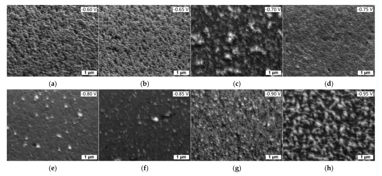
An SEM analysis was performed on each sample (Figure 2a–h). The deposition was not fully homogeneous but appeared to be quite smooth considering that to obtain an appreciable image the stage had to be tilted of 45° and the contrast was set to almost maximum. Such difficulties could be also attributed in part to the low thickness of the coatings (around 10 nm).
Figure 2.
SEM images using the stage tilted of 45° of the samples of CdSe obtained ad the following potentials: (a) −0.60 V; (b) −0.65 V; (c) −0.70 V; (d) −0.75 V; (e) −0.80 V; (f) −0.85 V; (g) −0.90 V; (h) −0.95 V.
Samples obtained with a potential of −0.60 V (a) and −0.65 V (b) present come holes on the surface, attributable to the non-fusion of the growth nuclei, probably caused by the low deposition potential. Samples realized with a deposition potential between −0.70 V and −0.90 V are quite uniform and similar one to each other. The deposition performed at −0.95 V shows the formation of several clusters; comparing this result with the electrochemical data, we suppose their reflects excess of Cd deposited at higher overpotentials.
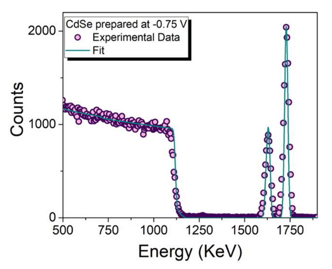
The samples were analysed with RBS (Figure 3) to obtain the amount of Cd and Se present on the sample. RBS allows for measuring the surface atomic concentration (atm ∗ cm−2) of cadmium and selenium on the electrode. With the surface atomic concentration, it is possible to determine two very important characteristics of the samples: the stoichiometric ratio and the thickness. Considering the stoichiometric ratio 1:1 in CdSe the equivalent amount of cadmium selenide was deduced (Equation (1)), excluding the excess of Se or Cd.
| (1) |
Figure 3.
RBS analysis of the CdSe sample prepared at −0.75 V on the Si substrate.
We found that the percentage of CdSe is >99% for deposition potential was lower than −0.70 V (Table 1). At a lower overpotential, we obtained an excess of selenium. Using only this information, it is not possible to distinguish if CdSe is deposited or if the elements are present in the form of Cd0 and Se0. From the electrochemical measurements, we observed that for a potential lower than −0.80 V, an excess of Cd was deposited as observed from the stripping voltammetry (Figure 1c).
Table 1.
Atomic density and thickness obtained from RBS analysis of the films prepared at different potentials.
| V Dep | Cd | Se | %CdSe | Thickness | |
|---|---|---|---|---|---|
| × 1016 atm ∗ cm−2 | CdSe (nm) | ε% | |||
| −0.60 | 1.78 | 2.86 | 76.7% | 9.7 | 44.8% |
| −0.65 | 0.70 | 1.92 | 53.4% | 3.8 | 17.6% |
| −0.70 | 3.10 | 3.09 | 99.8% | 16.9 | 77.7% |
| −0.75 | 2.57 | 2.55 | 99.6% | 13.9 | 64.1% |
| −0.80 | 2.07 | 2.10 | 99.3% | 11.3 | 52.1% |
| −0.85 | 1.73 | 1.75 | 99.4% | 9.4 | 43.5% |
| −0.90 | 1.17 | 1.37 | 92.1% | 6.4 | 29.4% |
| −0.95 | 1.69 | 1.68 | 99.7% | 9.2 | 42.3% |
RBS is also an established technique for the determination of the thickness [47], and by knowing the surface atomic concentration and the density of the deposit, it is easy to calculate the thickness of the coating (Equation (2)):
| (2) |
where NA is the Avogadro number, ρ the density and M the molar mass.
Considering the density of the compound and the geometric area of the electrode the equivalent thickness was calculated and the efficiency (ε%) (Equation (3)) was obtained by comparing the experimental value of the sample (tCdSe) with the theoretical one (tt).
| (3) |
The theoretical thickness was calculated using the Faraday law (Equation (4)) considering the amount of deposited charge (Q = 30 mC), the molar mass (M = 191.37 g/mol) and density (ρ = 5.82 g/cm3) of CdSe, the area of the electrode (A = 0.785 cm2), the number of electrons (n = 6) and the Faraday constant (F = 96,485 C/mol).
| (4) |
The deposition potential of −0.70 and −0.75 V produced the highest deposition thickness with the highest deposition efficiency. From these results, we decided to elect the −0.75 V as the best operating condition to obtain the CdSe film on n-Si. In the RBS spectrum of the −0.75 V CdSe sample is reported showing the experimental data along with the obtained fit.
We prepare fresh samples using this potential and we performed XRD and PL on the samples as prepared and after annealing treatment.
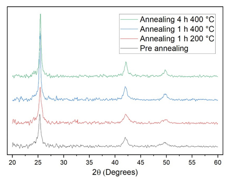
Samples prepared using a potential of −0.75 V were annealed under N2 atmosphere using the following conditions: 1 h at 200 °C, 1 h at 400 °C, or 4 h at 400 °C. Then, the crystallinity of the samples was investigated with XRD (Figure 4). The as-prepared sample shows the peaks characteristic of cubic CdSe at 25.5°, 42.2, and 49.9° [48,49]. No other signal was observed, meaning that the stoichiometric ratio between the two elements was satisfied. After annealing at 200 °C, we did not observe any substantial change. In both the two diffractograms recorded on the samples annealed at 400 °C, the peaks are more intense and sharper, even if the change in intensity does not differ considerably from the pre-annealed sample. Moreover, the number of peaks and their position remains unaltered. The low intensity and the lower number of peaks compared to bulk CdSe can be assigned to the very low amount of deposited substance. These results suggest that the thermal treatment favours a rearrangement of the atoms towards a more crystalline structure, but also the deposited films were not completely amorphous. Since the peaks do not change their positions we can assert that we do not have a change in crystalline structure from cubic to hexagonal, as sometimes observed by other authors [50,51,52]. In particular, we did not observe any variation at 23.9° in correspondence of the most intense and characteristic [100] peak of the hexagonal CdSe. No substantial differences were observed between the two different annealing time at 400 °C.
Figure 4.
XRD analysis of CdSe samples prepared with a potential of −0.75 V (black) and then annealed under N2 atmosphere for 1 h at 200 °C (red), 1 h at 400 °C (blue), or 4 h at 400 °C (green).
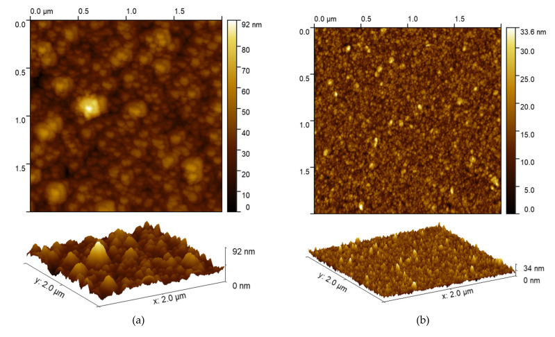
An AFM analysis was performed on the sample prepared with a deposition potential of −0.75 V, as growth was observed and after the 4 h thermal annealing performed at 400 °C (Figure 5). After the heat treatment, we observed a change in roughness, and after annealing the sample was flatter with a decreasing in roughness of almost three times while the maximum peak height dropped from 92 nm to 33.6 nm, while the RMS roughness (Sq) decreased from 9 nm to 3.5 nm. Considering that from the XRD measurements there is only a slight improvement of the crystallinity we can deduce that there is an arrangement of the matter towards a flatter condition, but the size of the grains does not change much.
Figure 5.
2D and 3D AFM analysis of the sample prepared at −0.75 V before (a) and after the 4 h annealing performed at 400 °C (b).
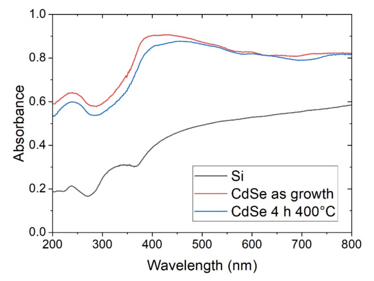
The absorption spectra of the silicon substrate and of the CdSe were recorded before and after the heat treatment (Figure 6). We observed that the deposit has a much higher absorbance than the substrate. Instead, the annealing leads to a slight decrease in absorption. The variations in absorbance seem to confirm the results obtained with the AFM and XRD measurements, i.e., the annealing process leads only to a variation of surface morphology and therefore of scattering.
Figure 6.
Absorbance spectra of the silicon substrate (black) and the sample prepared at −0.75 V: as growth (red) and after the 4 h annealing performed at 400 °C (blue).
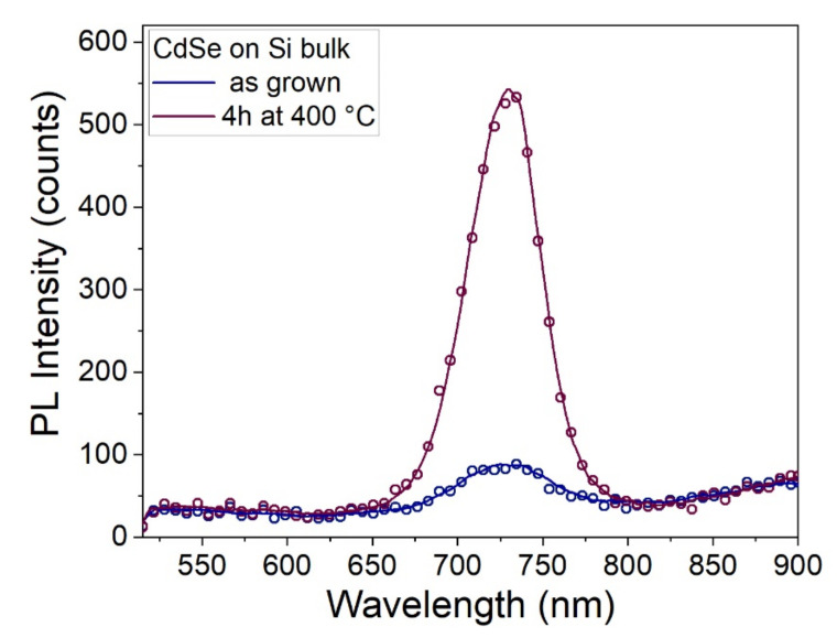
The photoluminescence spectrum of a sample prepared with a potential of −0.75 V was measured before and after the annealing at 400 °C for 4 h. The sample was excited with a 476 nm laser and the emission spectrum was recorded (more details in the experimental methods). After the annealing, the characteristic line shape of the emission peak of CdSe at 725 nm [53] remained unchanged but its intensity grew considerably by almost an order of magnitude in relation to the increase in crystallinity (Figure 7).
Figure 7.
Photoluminescence spectra of the sample prepared at −0.75 V before (blue) and after (claret violet) the annealing at 400 °C for 4 h, using an excitation laser with a wavelength of 476 nm.
4. Conclusions
In this work, the optimal conditions for the deposition of a CdSe film on n-Si were achieved using a potential of −0.75 V and a solution of Na2SeO3 and 3CdSO4∙8H2O in sulfuric acid electrolyte. At an overpotential of lower than −0.70 V, an excess of Se was detected with RBS analysis, while at an overpotential of greater than −0.80, an excess of Cd was evaluated from electrochemical stripping voltammetry and SEM images. The crystallinity and photoemission of the samples were evaluated and, even if the electrodeposition provides a crystalline deposit, we found that after annealing at 400 °C under a nitrogen atmosphere, the PL increased by almost an order of magnitude. The electrochemical deposition is an easy and cost-effective preparation method and the results obtained in this study suggest that it could also be applied to the silicon-manufacturing processes for the realization of optoelectronic devices.
Author Contributions
Conceptualization, W.G. and A.I.; formal analysis, M.V., A.A.L. and M.J.L.F.; data curation, M.V., A.A.L. and M.J.L.F.; writing—original draft preparation, W.G., M.V., A.A.L., M.J.L.F. and A.I.; writing—review and editing, W.G. and A.I.; supervision, W.G. and A.I.; project administration, M.I.; funding acquisition, M.I. All authors have read and agreed to the published version of the manuscript.
Funding
This research was funded by Regione Toscana POR CreO FESR 2014–2020—azione 1.1.5 sub-azione a1—Bando 1 “Progetti Strategici di ricerca e sviluppo” which made possible the project “Galvanica a basso impatto ambientale in ottica Industria 4.0” (GoodGalv), CUP 3647.04032020.157000060, CIPE D44E20003540009 and PRIN (“Progetti di Ricerca di Rilevante Interesse Nazionale”) which made possible the project “Novel Multilayered and Micro-Machined Electrode Nano-Architectures for Electrocatalytic Applications (Fuel Cells and Electrolyzers)”, grant number 2017YH9MRK. MIUR-Italy is also acknowledged for “Progetto Dipartimenti di Eccellenza 2018–2022” allocated to the Department of Chemistry “Ugo Schiff” of the University of Firenze, Italy.
Institutional Review Board Statement
Not applicable.
Informed Consent Statement
Not applicable.
Data Availability Statement
Data are contained within the article.
Conflicts of Interest
The authors declare no conflict of interest.
Footnotes
Publisher’s Note: MDPI stays neutral with regard to jurisdictional claims in published maps and institutional affiliations.
References
- 1.Kalem S., Werner P., Talalaev V. Near-IR photoluminescence from Si/Ge nanowire-grown silicon wafers: Effect of HF treatment. Appl. Phys. A Mater. Sci. Process. 2013;112:561–567. doi: 10.1007/s00339-013-7783-3. [DOI] [Google Scholar]
- 2.Wu K., Sun W., Jiang Y., Chen J., Li L., Cao C., Shi S., Shen X., Cui J. Structure and photoluminescence study of silicon based two-dimensional Si2Te3 nanostructures. J. Appl. Phys. 2017;122:075701. doi: 10.1063/1.4998811. [DOI] [Google Scholar]
- 3.Iatsunskyi I., Pavlenko M., Viter R., Jancelewicz M., Nowaczyk G., Baleviciute I., Załęski K., Jurga S., Ramanavicius A., Smyntyna V. Tailoring the Structural, Optical, and Photoluminescence Properties of Porous Silicon/TiO2 Nanostructures. J. Phys. Chem. C. 2015;119:7164–7171. doi: 10.1021/acs.jpcc.5b01670. [DOI] [Google Scholar]
- 4.Iacona F., Pacifici D., Irrera A., Miritello M., Franzò G., Priolo F., Sanfilippo D., Di Stefano G., Fallica P.G. Electroluminescence at 1.54 μm in Er-doped Si nanocluster-based devices. Appl. Phys. Lett. 2002;81:3242–3244. doi: 10.1063/1.1516235. [DOI] [Google Scholar]
- 5.Talbot E., Lardé R., Pareige P., Khomenkova L., Hijazi K., Gourbilleau F. Nanoscale evidence of erbium clustering in Er-doped silicon-rich silica. Nanoscale Res. Lett. 2013;8:1–8. doi: 10.1186/1556-276X-8-39. [DOI] [PMC free article] [PubMed] [Google Scholar]
- 6.Gao Y., Shen H., Cao J., Li D., Yang D. Control of the formation and luminescent properties of polymorphic erbium silicates on silicon. Opt. Mater. Express. 2019;9:1716. doi: 10.1364/OME.9.001716. [DOI] [Google Scholar]
- 7.Leonardi A.A., Lo Faro M.J., Irrera A. CMOS-Compatible and Low-Cost Thin Film MACE Approach for Light-Emitting Si NWs Fabrication. Nanomaterials. 2020;10:966. doi: 10.3390/nano10050966. [DOI] [PMC free article] [PubMed] [Google Scholar]
- 8.Walavalkar S.S., Hofmann C.E., Homyk A.P., Henry M.D., Atwater H.A., Scherer A. Tunable visible and near-IR emission from sub-10 nm etched single-crystal Si nanopillars. Nano Lett. 2010;10:4423–4428. doi: 10.1021/nl102140k. [DOI] [PubMed] [Google Scholar]
- 9.Dohnalová K., Poddubny A.N., Prokofiev A.A., De Boer W.D., Umesh C.P., Paulusse J.M., Zuilhof H., Gregorkiewicz T. Surface brightens up Si quantum dots: Direct bandgap-like size-tunable emission. Light Sci. Appl. 2013;2:e47. doi: 10.1038/lsa.2013.3. [DOI] [Google Scholar]
- 10.Leonardi A.A., Nastasi F., Morganti D., Lo Faro M.J., Picca R.A., Cioffi N., Franzò G., Serroni S., Priolo F., Puntoriero F., et al. New Hybrid Light Harvesting Antenna Based on Silicon Nanowires and Metal Dendrimers. Adv. Opt. Mater. 2020;8:2001070. doi: 10.1002/adom.202001070. [DOI] [Google Scholar]
- 11.Lo Faro M.J., Leonardi A.A., Priolo F., Fazio B., Miritello M., Irrera A. Erbium emission in Er:Y2O3 decorated fractal arrays of silicon nanowires. Sci. Rep. 2020;10:12854. doi: 10.1038/s41598-020-69864-5. [DOI] [PMC free article] [PubMed] [Google Scholar]
- 12.Karbassian F., Rajabali S., Chimeh A., Mohajerzadeh S., Asl-Soleimani E. Luminescent porous silicon prepared by reactive ion etching. J. Phys. D. Appl. Phys. 2014;47:385103. doi: 10.1088/0022-3727/47/38/385103. [DOI] [Google Scholar]
- 13.Gelloz B., Juangsa F.B., Nozaki T., Asaka K., Koshida N., Jin L. Si/SiO2 Core/Shell Luminescent Silicon Nanocrystals and Porous Silicon Powders With High Quantum Yield, Long Lifetime, and Good Stability. Front. Phys. 2019;7:47. doi: 10.3389/fphy.2019.00047. [DOI] [Google Scholar]
- 14.Tsybeskov L., Lockwood D.J. Silicon-germanium nanostructures for light emitters and on-chip optical interconnects. Proc. IEEE. 2009;97:1284–1303. doi: 10.1109/JPROC.2009.2020711. [DOI] [Google Scholar]
- 15.Hambrock J., Birkner A., Fischer R.A. Synthesis of CdSe nanoparticles using various organometallic cadmium precursors. J. Mater. Chem. 2001;11:3197–3201. doi: 10.1039/b104231a. [DOI] [Google Scholar]
- 16.Ge Y., Zhang M., Wang L., Meng L., Tang J., Chen Y., Wang L., Zhong H. Polarization-Sensitive Ultraviolet Detection from Oriented-CdSe@CdS-Dot-in-Rods-Integrated Silicon Photodetector. Adv. Opt. Mater. 2019;7:1–7. doi: 10.1002/adom.201900330. [DOI] [Google Scholar]
- 17.Sun M., Zhang S., Wang J., Jia Z., Lv X., Huang X. Enhanced biosensor based on assembled porous silicon microcavities using CdSe/ZnS quantum dots. IEEE Photonics J. 2021;13:1–6. doi: 10.1109/JPHOT.2021.3101656. [DOI] [Google Scholar]
- 18.Li K., Lin X., Song B., Kondrotas R., Wang C., Lu Y., Yang X., Chen C., Tang J. Rapid thermal evaporation for cadmium selenide thin-film solar cells. Front. Optoelectron. 2021;14:482–490. doi: 10.1007/s12200-021-1217-1. [DOI] [PMC free article] [PubMed] [Google Scholar]
- 19.Lopez-Delgado R., Zhou Y., Zazueta-Raynaud A., Zhao H., Pelayo J.E., Vomiero A., Álvarez-Ramos M.E., Rosei F., Ayon A. Enhanced conversion efficiency in Si solar cells employing photoluminescent down-shifting CdSe/CdS core/shell quantum dots. Sci. Rep. 2017;7:14104. doi: 10.1038/s41598-017-14269-0. [DOI] [PMC free article] [PubMed] [Google Scholar]
- 20.Zhao J., Bardecker J.A., Munro A.M., Liu M.S., Niu Y., Ding I.K., Luo J., Chen B., Jen A.K.Y., Ginger D.S. Efficient CdSe/CdS quantum dot light-emitting diodes using a thermally polymerized hole transport layer. Nano Lett. 2006;6:463–467. doi: 10.1021/nl052417e. [DOI] [PubMed] [Google Scholar]
- 21.Pal B.N., Ghosh Y., Brovelli S., Laocharoensuk R., Klimov V.I., Hollingsworth J.A., Htoon H. ‘Giant’ CdSe/CdS Core/Shell Nanocrystal Quantum Dots As Efficient Electroluminescent Materials: Strong Influence of Shell Thickness on Light-Emitting Diode Performance. Nano Lett. 2011;12:331–336. doi: 10.1021/nl203620f. [DOI] [PubMed] [Google Scholar]
- 22.Bae W.K., Kwak J., Park J.W., Char K., Lee C., Lee S. Highly Efficient Green-Light-Emitting Diodes Based on CdSe@ZnS Quantum Dots with a Chemical-Composition Gradient. Adv. Mater. 2009;21:1690–1694. doi: 10.1002/adma.200801908. [DOI] [Google Scholar]
- 23.Tarabrin M.K., Ustinov D.V., Tomilov S.M., Lazarev V.A., Karasik V.E., Kozlovsky V.I., Korostelin Y.V., Skasyrsky Y.K., Frolov M.P. Proceedings of the Laser Congress 2018 (ASSL) Optical Society of America; Boston, MA, USA: 2018. Highly efficient continuous wave single mode Cr:CdSe laser with output power more than 2 W; p. AW3A.8. [Google Scholar]
- 24.Kozlovsky V.I., Korostelin Y.V., Podmar’kov Y.P., Skasyrsky Y.K., Frolov M.P. Middle infrared Fe2+:ZnS, Fe2+:ZnSe and Cr2+:CdSe lasers: New results. J. Phys. Conf. Ser. 2016;740:012006. doi: 10.1088/1742-6596/740/1/012006. [DOI] [Google Scholar]
- 25.Akimov V.A., Kozlovskii V.I., Korostelin Y.V., Landman A.I., Podmar’kov Y.P., Skasyrskii Y.K., Frolov M.P. Efficient pulsed Cr2+:CdSe laser continuously tunable in the spectral range from 2.26 to 3.61 μm. Quantum Electron. 2008;38:205. doi: 10.1070/QE2008v038n03ABEH013707. [DOI] [Google Scholar]
- 26.Ayvazian T., van der Veer W.E., Xing W., Yan W., Penner R.M. Electroluminescent, Polycrystalline Cadmium Selenide Nanowire Arrays. ACS Nano. 2013;7:9469–9479. doi: 10.1021/nn4043546. [DOI] [PubMed] [Google Scholar]
- 27.Ramrakhiani M., Nogriya V. Photo- and electro-luminescence of cadmium selenide nanocrystals and nanocomposites. J. Lumin. 2013;133:129–134. doi: 10.1016/j.jlumin.2011.09.046. [DOI] [Google Scholar]
- 28.Freeman R., Finder T., Bahshi L., Gill R., Willner I. Functionalized CdSe/ZnS QDs for the detection of nitroaromatic or RDX explosives. Adv. Mater. 2012;24:6416–6421. doi: 10.1002/adma.201202793. [DOI] [PubMed] [Google Scholar]
- 29.Zhang Y., Xiao J.-Y., Zhu Y., Tian L.-J., Wang W.-K., Zhu T.-T., Li W.-W., Yu H.-Q. Fluorescence Sensor Based on Biosynthetic CdSe/CdS Quantum Dots and Liposome Carrier Signal Amplification for Mercury Detection. Anal. Chem. 2020;92:3990–3997. doi: 10.1021/acs.analchem.9b05508. [DOI] [PubMed] [Google Scholar]
- 30.Sung T.W., Lo Y.L. Ammonia vapor sensor based on CdSe/SiO2 core–shell nanoparticles embedded in sol–gel matrix. Sensors Actuators B Chem. 2013;188:702–708. doi: 10.1016/j.snb.2013.07.040. [DOI] [Google Scholar]
- 31.Li Z., Peng X. Size/Shape-Controlled Synthesis of Colloidal CdSe Quantum Disks: Ligand and Temperature Effects. J. Am. Chem. Soc. 2011;133:6578–6586. doi: 10.1021/ja108145c. [DOI] [PubMed] [Google Scholar]
- 32.Baek S.-W., Shim J.-H., Seung H.-M., Lee G.-S., Hong J.-P., Lee K.-S., Park J.-G. Effect of core quantum-dot size on power-conversion-efficiency for silicon solar-cells implementing energy-down-shift using CdSe/ZnS core/shell quantum dots. Nanoscale. 2014;6:12524–12531. doi: 10.1039/C4NR02472A. [DOI] [PubMed] [Google Scholar]
- 33.Nguyen H.T., Tran T.T., Bhatt V., Kumar M., Song J., Yun J.-H. Enhancement of Schottky Junction Silicon Solar Cell with CdSe/ZnS Quantum Dots Decorated Metal Nanostructures. Appl. Sci. 2021;12:83. doi: 10.3390/app12010083. [DOI] [Google Scholar]
- 34.Kim J., Choi S., Noh J., Yoon S., Lee S., Noh T., Frank A.J., Hong K. Synthesis of CdSe−TiO 2 Nanocomposites and Their Applications to TiO 2 Sensitized Solar Cells. Langmuir. 2009;25:5348–5351. doi: 10.1021/la804310z. [DOI] [PubMed] [Google Scholar]
- 35.Li Z., Jin D., Wang Z. Synthesis of step-scheme In2Se3/CdSe nanocomposites photocatalysts for hydrogen production. Compos. Commun. 2021;24:100618. doi: 10.1016/j.coco.2020.100618. [DOI] [Google Scholar]
- 36.Shaikh A.V., Mane R.S., Joo O.S., Han S.H., Pathan H.M. Electrochemical deposition of cadmium selenide films and their properties: A review. J. Solid State Electrochem. 2017;21:2517–2530. doi: 10.1007/s10008-017-3552-0. [DOI] [Google Scholar]
- 37.Kowalik R., Kazimierczak H., Zabiński P. Electrodeposition of cadmium selenide. Mater. Sci. Semicond. Process. 2016;50:43–48. doi: 10.1016/j.mssp.2016.04.009. [DOI] [Google Scholar]
- 38.Loglio F., Innocenti M., D’Acapito F., Felici R., Pezzatini G., Salvietti E., Foresti M.L. Cadmium selenide electrodeposited by ECALE: Electrochemical characterization and preliminary results by EXAFS. J. Electroanal. Chem. 2005;575:161–167. doi: 10.1016/j.jelechem.2004.09.007. [DOI] [Google Scholar]
- 39.Foresti M.L., Milani S., Loglio F., Innocenti M., Pezzatini G., Cattarin S. Ternary CdS x Se 1 x Deposited on Ag(111) by ECALE: Synthesis and Characterization. Langmuir. 2005;21:6900–6907. doi: 10.1021/la050176k. [DOI] [PubMed] [Google Scholar]
- 40.Salvietti E., Giurlani W., Foresti M.L., Passaponti M., Fabbri L., Marcantelli P., Caporali S., Martinuzzi S., Calisi N., Pedio M., et al. On the Contrasting Effect Exerted by a Thin Layer of CdS against the Passivation of Silver Electrodes Coated with Thiols. Surfaces. 2018;1:29–42. doi: 10.3390/surfaces1010004. [DOI] [Google Scholar]
- 41.Vizza M., Giaccherini A., Giurlani W., Passaponti M., Cioffi N., Picca R.A., De Luca A., Fabbri L., Lavacchi A., Gambinossi F., et al. Successes and Issues in the Growth of Moad and MoSe2 on Ag(111) by the E-ALD Method. Metals. 2019;9:122. doi: 10.3390/met9020122. [DOI] [Google Scholar]
- 42.Giurlani W., Giaccherini A., Calisi N., Zangari G., Salvietti E., Passaponti M., Caporali S., Innocenti M. Investigations on the Electrochemical Atomic Layer Growth of Bi2Se3 and the Surface Limited Deposition of Bismuth at the Silver Electrode. Materials. 2018;11:1426. doi: 10.3390/ma11081426. [DOI] [PMC free article] [PubMed] [Google Scholar]
- 43.Giurlani W., Dell’Aquila V., Vizza M., Calisi N., Lavacchi A., Irrera A., Lo Faro M.J., Leonardi A.A., Morganti D., Innocenti M. Electrodeposition of Nanoparticles and Continuous Film of CdSe on n-Si (100) Nanomaterials. 2019;9:1504. doi: 10.3390/nano9101504. [DOI] [PMC free article] [PubMed] [Google Scholar]
- 44.Forni F., Innocenti M., Pezzatini G., Foresti M. Electrochemical aspects of CdTe growth on the face (111) of silver by ECALE. Electrochim. Acta. 2000;45:3225–3231. doi: 10.1016/S0013-4686(00)00426-6. [DOI] [Google Scholar]
- 45.Lewandowski C.M., Co-investigator N., Lewandowski C.M., Zhang X.G. Electrochemistry of Silicon and its Oxide. Eff. Br. Mindfulness Interv. Acute Pain Exp. An Exam. Individ. Differ. 2015;1:1689–1699. doi: 10.1017/CBO9781107415324.004. [DOI] [Google Scholar]
- 46.Chubenko E.B., Klyshko A.A., Petrovich V.A., Bondarenko V.P. Electrochemical deposition of zinc selenide and cadmium selenide onto porous silicon from aqueous acidic solutions. Thin Solid Films. 2009;517:5981–5987. doi: 10.1016/j.tsf.2009.03.134. [DOI] [Google Scholar]
- 47.Seah M.P., Spencer S.J., Bensebaa F., Vickridge I., Danzebrink H., Krumrey M., Gross T., Oesterle W., Wendler E., Rheinländer B., et al. Critical review of the current status of thickness measurements for ultrathin SiO2 on Si Part V: Results of a CCQM pilot study. Surf. Interface Anal. 2004;36:1269–1303. doi: 10.1002/sia.1909. [DOI] [Google Scholar]
- 48.Chen M.L., Oh W.C. Synthesis and highly visible-induced photocatalytic activity of CNT-CdSe composite for methylene blue solution. Nanoscale Res. Lett. 2011;6:1–8. doi: 10.1186/1556-276X-6-398. [DOI] [PMC free article] [PubMed] [Google Scholar]
- 49.Sapra S., Rogach A.L., Feldmann J. Phosphine-free synthesis of monodisperse CdSe nanocrystals in olive oil. J. Mater. Chem. 2006;16:3391–3395. doi: 10.1039/b607022a. [DOI] [Google Scholar]
- 50.Kale R.B., Lokhande C.D. Influence of air annealing on the structural, optical and electrical properties of chemically deposited CdSe nano-crystallites. Appl. Surf. Sci. 2004;223:343–351. doi: 10.1016/j.apsusc.2003.09.022. [DOI] [Google Scholar]
- 51.Mahato S., Kar A.K. The effect of annealing on structural, optical and photosensitive properties of electrodeposited cadmium selenide thin films. J. Sci. Adv. Mater. Devices. 2017;2:165–171. doi: 10.1016/j.jsamd.2017.04.001. [DOI] [Google Scholar]
- 52.Zapata-Torres M., Chale-Lara F., Caballero-Briones F., Calzadilla O. Effect of annealing temperature on the crystalline quality and phase transformation of Chemically Deposited CdSe films. Phys. Status Solidi C Conf. 2005;2:3742–3745. doi: 10.1002/pssc.200461804. [DOI] [Google Scholar]
- 53.Semaltianos N.G., Logothetidis S., Perrie W., Romani S., Potter R.J., Sharp M., French P., Dearden G., Watkins K.G. CdSe nanoparticles synthesized by laser ablation. EPL. 2008;84:47001. doi: 10.1209/0295-5075/84/47001. [DOI] [Google Scholar]
Associated Data
This section collects any data citations, data availability statements, or supplementary materials included in this article.
Data Availability Statement
Data are contained within the article.


