

Abstract

Colloidal semiconductor nanoplatelets exhibit strong quantum confinement for electrons and holes as well as excitons in one dimension, while their in-plane motion is free. Because of the large dielectric contrast between the semiconductor and its ligand environment, the Coulomb interaction between electrons and holes is strongly enhanced. By means of one- and two-photon photoluminescence excitation spectroscopy, we measure the energies of the 1S and 1P exciton states in CdSe nanoplatelets with thicknesses varied from 3 up to 7 monolayers. By comparison with calculations, performed in the effective mass approximation with account of the dielectric enhancement, we evaluate exciton binding energies of 195–315 meV, which is about 20 times greater than that in bulk CdSe. Our calculations of the effective Coulomb potential for very thin nanoplatelets are close to the Rytova-Keldysh model, and the exciton binding energies are comparable with the values reported for monolayer-thick transition metal dichalcogenides.
Keywords: nanoplatelets, CdSe, exciton binding energy, two-photon absorption
The shape of colloidal nanostructures strongly modifies the exciton properties. In bulk, excitons are hydrogen-like quasiparticles with free center-of-mass motion in all directions. In quantum dots, electrons and holes are fully confined, and therefore the exciton they form is immobile.1 Two-dimensional colloidal nanoplatelets (NPLs) have a thickness of only several atomic layers but much larger in-plane extensions.2,3 That is, the exciton confinement is extremely strong in the direction perpendicular to the NPL plane, while the in-plane motion is free. CdSe NPLs have remarkable optical properties with narrow emission lines,4,5 low lasing threshold, strong optical gain,6,7 and large multiphoton absorption cross section.8,9 A wide variety of spin phenomena has recently been reported for NPLs.10−14 The exciton with its large binding energy dominates the optical properties of CdSe NPLs. Therefore, comprehensive information on the exciton parameters is important. In bulk CdSe, the exciton binding energy is only Eb3D = 15 meV. In NPLs, it exceeds the two-dimensional (2D) limit of 4Eb = 60 meV and reaches hundreds of meV. This is because the Coulomb forces are inversely proportional to the dielectric constant of the medium and act in all three dimensions, so that the electric field lines are not restricted to the NPL with comparatively high dielectric constant but penetrate into the surrounding medium (ligands, solvent) with low dielectric constant. As a result, the electron–hole interaction is strongly renormalized by the dielectric enhancement effect. To determine the exciton binding energy, one needs to measure the difference between the ground exciton state (1S) energy and the bandgap. While the 1S state in CdSe NPLs can be addressed optically, bandgap measurements are more complicated because of the weak oscillator strength of band-to-band transitions. Alternatively, one can measure optically the energies of two or more excitonic states and in combination with modeling derive the binding energy. The first approach was recently reported by two pioneering papers. Zelewski et al. probed the band-to-band transition by photoacoustics,15 and Ji et al. addressed the electronic density of states by scanning tunneling spectroscopy.16 The reported binding energies differ significantly: 130–230 meV in NPLs with thickness ranging from 5 to 3 monolayers (MLs) as reported in ref (15) versus 280–420 meV in NPLs with 7 to 3 ML thickness in ref (16). The theoretical predictions also scatter. Benchamekh et al.17 utilized tight-binding calculations and effective mass approximation and reported 216–413 and 149–289 meV in 7 to 3 ML thick NPLs for two different values of the CdSe high frequency dielectric constant. Brumberg et al.18 used the pseudopotential method to solve the Bethe-Salpeter equation and obtained 170–210 meV binding energy in 5–3 ML NPLs. Obviously, more studies and additional approaches are needed to clarify the electron–hole interaction in NPLs. Also, relatively simple model approaches allowing one to predict the exciton parameters in NPLs are in great need. In this manuscript, we provide both new experimental results and a detailed theoretical model.
In detail, we measure directly the transition energies of the 1S and 1P exciton states in 3, 4, 5, and 7 monolayer thick CdSe NPLs. Here, the first number in the exciton denomination indicates the order in energy within a series of exciton states of fixed orbital angular momentum, S or P, with unity indicating the ground state. The 1S and 1P states have different symmetry and can be excited by one and two photons, respectively. From the 1P–1S energy splitting, we evaluate the exciton binding energy, which ranges from 195 meV in 7 ML NPLs up to 315 meV in 3 ML NPLs. For this, we calculate the exciton energy level structure within the effective mass approximation, accounting for the dielectric enhancement effect. From the model, we obtain Coulomb potentials for thin layers, which account for the charge distributions normal to the NPL plane. By comparing the calculations of the exciton binding energy with the experimental data, we obtain the value of the dielectric constant inside the nanoplatelet εin = 6 at the frequency corresponding to the binding energy.
Experimental Results
The parameters of the studied CdSe NPLs are given in Table 1. The CdSe NPLs are Cd-terminated and have thicknesses of 3.5, 4.5, 5.5, and 7.5 monolayers (MLs). They were synthesized by colloidal chemistry according to the protocols reported in ref (19) (3 ML), ref (2) (4 and 5 ML), and ref (5) (7 ML).
Table 1. Exciton Energies in CdSe Nanoplatelets Measured at T = 4.2 Ka.
| sample label | 3 ML | 4 ML | 5 ML | 7 ML |
|---|---|---|---|---|
| NPL thickness (ML) | 3.5 | 4.5 | 5.5 | 7.5 |
| NPL thickness, L (nm) | 1.05 | 1.35 | 1.65 | 2.25 |
| exciton emission energy (eV) | 2.497 | 2.319 | 2.115 | |
| trion emission energy (eV) | 2.729 | 2.477 | 2.301 | 2.098 |
| 1S energy (eV) | 2.778 ± 0.006 | 2.512 ± 0.004 | 2.332 ± 0.003 | 2.155 ± 0.007 |
| 1P energy (eV) | 2.992 ± 0.015 | 2.693 ± 0.013 | 2.49 ± 0.011 | 2.275 ± 0.023 |
| 1P–1S splitting (meV) | 214 ± 21 | 181 ± 17 | 154 ± 14 | 120 ± 30 |
| 1P–1S splitting (meV), model | 212 | 177 | 153 | 121 |
| exciton binding energy (meV), model | 315 | 270 | 240 | 195 |
Calculations within the effective mass approximation were made with εin = 6 and εout = 2.
Low-temperature photoluminescence (PL) spectra of the dropcasted NPL samples are shown in Figure 1a. Except for the 3 ML NPLs, in each case the spectrum consists of two narrow lines: the higher energy line corresponds to the exciton emission and the lower energy one to the emission of negatively charged excitons (trions). The experimental identification of these lines was reported in refs (20) and (21). In the 3 ML NPLs, the emission is broadened due to the lateral sizes inhomogeneity so that exciton and trion emission overlap, and the PL peak corresponds to the trion emission. The energies of the exciton and trion lines are given in Table 1. Their large spectral shift, from about 2.10 eV in the 7 ML NPLs up to 2.73 eV in the 3 ML NPLs is mainly contributed by the increase of the quantum confinement energies of electrons and holes, which is partly compensated by an increase of the exciton binding energy in the thinner NPLs.
Figure 1.

(a) Photoluminescence spectra of CdSe NPLs measured at T = 4.2 K for nonresonant excitation with 3.06 eV photon energy. (b) PL, 1-PLE, and 2-PLE spectra of 5 ML NPLs. The exciton emission line (X), and the 1S and 1P energies are marked by arrows. 1Slh is contributed by the light holes. Red lines and the blue arrow show the evaluation of the 1P exciton energy by the tangent method (Supporting Information (SI) Section S5). (c) Schematics of one-photon and two-photon absorption. One-photon excitation couples to the 1S exciton with lz = 0, while two-photon excitation creates the 1P exciton with lz = ±1.
Figure 1b shows PL and PL excitation (PLE) spectra of the 5 ML NPLs. Similar data for the other samples are given in the Figure S1. The exciton emission (red arrow) is centered at the energy of 2.319 eV. The green squares represent the one-photon PL excitation (1-PLE) spectrum detected at 2.230 eV, while the laser photon energy was tuned from 2.25 up to 2.60 eV (SI Section S5). The first absorption peak, which corresponds to the ground 1S exciton state, is at the energy of 2.332 eV. The small Stokes shift between the exciton lines in PL and PLE spectra of only 13 meV is typical for CdSe NPLs. The second broad peak at 2.45 eV marked as 1Slh is contributed by the light holes.
The one-photon optical transition from valence to conduction band is accompanied by a change of the total orbital angular momentum |Δjz| = 1. Because of the P- and S-type character of the valence band and conduction band Bloch states, the one-photon transition involves the change of the angular momentum of the Bloch states, while creating an exciton with zero orbital angular momentum of the relative motion (|lz| = 0), that is, with an S-type wave function (Figure 1c, left). In a two-photon excitation process (Figure 1c, right), the excess orbital momentum of the second photon is transferred to the envelope angular momentums of the exciton with the orbital quantum number |lz| = 1, that is, the created exciton has a P-type envelope wave function.
The two-photon PLE (2-PLE) spectrum is shown in Figure 1b by the blue circles. It is measured under the same conditions as the 1-PLE spectrum, but note the exciting laser energy scale for 2-PLE at the top of Figure 1b. The pronounced peak at the energy of 2.49 eV corresponds to the two-photon absorption edge, that is, the 1P exciton state. To determine the spectral position of the peak, we used the so-called tangent method (red lines in Figure 1b) described in the SI Section S5.
The transition energies of the 1S and 1P states measured for all samples are collected in Table 1 and shown in Figure 2a. Figure 2b (green squares) shows the 1P–1S splitting values together with the curve calculated according to our model (see below).
Figure 2.

Exciton energies in CdSe NPLs. (a) Experimentally measured energies of the 1S (red triangles) and 1P (blue stars) exciton states versus NPL thickness. (b) Energy splitting between the 1P and 1S exciton states, measured (green squares) and calculated (red line). (c) Exciton binding energy calculated within the model (red line). Blue circles: calculated exciton binding energy for NPLs with thickness as in our samples. Small red dots in panels b and c denote calculations for NPLs with thickness 3.5, 4.5, 5.5, 6.5, and 7.5 MLs.
Model
We performed numerical calculations of the exciton states in the NPLs within the effective mass approximation approach developed in refs (22) and (23). It includes the electron–hole Coulomb interaction and single particle potentials modified by the difference in dielectric constants inside and outside an NPL. We assumed that the hole mass is anisotropic with the in-plane mass mh∥ = 0.19m0 and the out-of-plane mass mh = 0.9m0, where m0 is the free electron mass. The anisotropy is in accord with a 6-band k·p model. The electron mass is obtained within an 8-band model, me∥ and me equal to 0.245m0 and 0.19m0, correspondingly, in 0.3 nm thick NPLs, and reduces to 0.14m0 and 0.13m0 in 2.3 nm thick NPLs (Figure S3).
We take the electron–hole Hamiltonian in the form
| 1 |
where H0 describes the noninteracting electron and hole, and Ueh accounts for the modified Coulomb interaction. More details on H0 are presented in the SI Section S3.1.
Ueh determines the exciton binding energy. Because of the extremely small NPL thickness, the electron–hole interaction is strongly renormalized by the dielectric enhancement effect. The electric field lines are not restricted to the NPL with high dielectric constant εin but penetrate into the surrounding medium with low dielectric constant εout (Figure 3a). The resulting potential classically is considered by introducing image charges. An example of a set of hole images is presented in Figure 3b. The interaction of the electron with the hole and all hole image charges results in an increase of the Coulomb interaction
| 2 |
where
| 3 |
Here ρ is the in-plane electron–hole
displacement: ρ = ρe – ρh, where ρe and ρh are the in-plane
positions of electron and hole, respectively (Figure 3c). ze and zh are electron and hole coordinates along the z-axis, normal to the NPL plane, respectively (Figure 3c). The image charges qn scale as  and
their positions can be found from zn+1+ = L – zn, zn+1– = −L – zn, z0+ = z0 = zh (Figure 3b). Here, the NPL is assumed to be positioned
between z = ±L/2, giving its
boundaries. More details are presented in the SI Section S3.1.
and
their positions can be found from zn+1+ = L – zn, zn+1– = −L – zn, z0+ = z0 = zh (Figure 3b). Here, the NPL is assumed to be positioned
between z = ±L/2, giving its
boundaries. More details are presented in the SI Section S3.1.
Figure 3.

(a) Schematic representation of the dielectric
enhancement effect.
The field lines do not remain confined to the NPL with high dielectric
constant εin but penetrate into the surrounding medium
with low dielectric constant εout so that the Coulomb
attraction is enhanced. (b) Schematic of image charges: the electron
interacts with the hole and all image charges created by the hole.
(c) In-plane coordinates of electrons, holes, and excitons. (d) Modified
Coulomb potential. 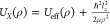 with lz = 0 and |lz|
= 1, for S (red) and P (green) exciton states in NPLs with 1.6 nm
thickness. Dashed lines show the Coulomb potentials of the point charges,
−e2/ερ, for the dielectric constants ε = 6 (gray), and ε =
2 (blue).
with lz = 0 and |lz|
= 1, for S (red) and P (green) exciton states in NPLs with 1.6 nm
thickness. Dashed lines show the Coulomb potentials of the point charges,
−e2/ερ, for the dielectric constants ε = 6 (gray), and ε =
2 (blue).
After separating the variables, the exciton wave function, which describes the motion of electron relative to hole, reads
| 4 |
Here An are coefficients; ξ1(ze) and ζ1(zh)
are the ground states of the one-dimensional (1D) Schrödinger
equation for electron and hole in z-direction, see eq S2; and  are the angular parts
of the cylindrical
harmonics, φ being the in-plane polar angle, and lz being the z-projection
of the orbital angular momentum of the relative electron–hole
motion. lz = 0 for the
S-states and ±1 for the P-states.
are the angular parts
of the cylindrical
harmonics, φ being the in-plane polar angle, and lz being the z-projection
of the orbital angular momentum of the relative electron–hole
motion. lz = 0 for the
S-states and ±1 for the P-states.
The projection of the Schrödinger eq 1 on the z-confined electron and hole states is
| 5 |
Here μ is the reduced exciton mass, 1/μ = 1/me∥+1/mh. Note that eq 5 is similar to a 2D hydrogen problem but has a non-Coulomb potential energy Ueff defined by the following equation
| 6 |
Figure 3d presents Ueff(ρ) for a 1.6 nm thick NPL plotted
by the red line. It follows a Coulomb-like potential – e2/ερ with ε
= εout for large electron–hole separations
(blue dashed line) but diverges for small separations. Importantly,
the attraction between electron and hole on short distances is weaker
than the Coulomb attraction in CdSe, the latter is equal to – e2/ερ with ε
= εin (gray dashed line). This is due to the integration
along the z-direction in eq 6. The green line gives  with lz = ±1 for the P-states.
On short distances between electron
and hole, it becomes large positive, which results from the centrifugal
potential acting for the P-type wave function (compare the wave functions
in Figure S2b,c). Ueff(ρ) for the NPLs with thicknesses of 0.3 and 2.3 nm
are plotted in Figure S4.
with lz = ±1 for the P-states.
On short distances between electron
and hole, it becomes large positive, which results from the centrifugal
potential acting for the P-type wave function (compare the wave functions
in Figure S2b,c). Ueff(ρ) for the NPLs with thicknesses of 0.3 and 2.3 nm
are plotted in Figure S4.
Exciton Binding Energy
Figure 4a,b displays the calculated 1S and 1P exciton binding energies plotted versus the inverse NPL thickness for different εin and εout (see the legend in panel b). The choice of the dielectic constant values is determined by the following consideration: it is a priori not clear, which εin for zinc-blende CdSe should be used. There are two possibilities: (i) the high-frequency CdSe dielectric constant ε∞ = 6, which is relevant for the case where the Coulomb energies of electron and hole are much larger than the energy of the optical phonon, and (ii) the background dielectric constant of CdSe εb = 8.4, which takes into account the contribution from all crystal excitations except the exciton. The εout value is given by the permittivity of the surrounding medium. As nanoplatelets are covered by organic ligands, it is challenging to determine their dielectric constant. Oleic acid itself has a static dielectric constant εout = 2.1 (for random orientation of the molecules).24 For oriented ligands, the dielectric tensor should be anisotropic but we neglect this effect.
Figure 4.

Exciton binding energies versus inverted NPL thickness calculated for various values of εin and εout given in the legend of panel (b). (a) Binding energy of the 1S exciton state. (b) Binding energy of the 1P exciton state. (c) 1P–1S splitting, here experimental values are shown by green squares. Small dots in all panels denote NPLs with thickness 1.5, 2.5, 3.5, 4.5, 5.5, 6.5, and 7.5 MLs.
The dielectric constants determine the screening of the Coulomb interaction by the NPL material and ligands. The smaller these constants, the larger the exciton binding energy (compare the red and blue solid and dashed lines in Figure 4a). Note that the green lines in Figure 4 are plotted for εout = εin. Small dots in Figure 4 denote NPLs with thickness 1.5, 2.5, 3.5, 4.5, 5.5, 6.5, and 7.5 MLs. Interestingly, the 1S exciton energies depend significantly on the dielectric constant of the surrounding medium εout even in thick NPLs with 2.3 nm width.
Figure 4c shows the calculated 1P–1S splitting by the lines, while the green squares are the experimentally measured data (taken from Figure 2b). We find good agreement between experiment and theory for εin = 6 and εout = 2. Importantly, the same set of parameters successfully describes another exciton characteristic energy, the bright-dark splitting in the same NPLs, which was measured in ref (20) (see SI Section S4). We conclude that εin = 6 and εout = 2 describe the exciton energy spectrum in effective mass approximation. Our model calculations with these parameters are also shown in Figure 2b,c (lines). Here the green squares give the measured 1P–1S splitting, and the circles are exciton binding energies for NPLs with thickness as in our samples. We take these values as the 1S exciton binding energies and list them in Table 1.
The evaluated exciton binding energies range from 195 meV in 7 ML NPLs up to 315 meV in 3 ML NPLs. Figure 5a compares our results (red points) with the literature data. Note that the horizontal axis in Figure 5a refers to the integer number of monolayers. To obtain the real thickness, 0.5 ML should be added. Although all data sets follow the same trend of the exciton binding energy increasing with decreasing NPL thickness, there are significant differences between them. Zelewski et al.15 reported values that are about 30% smaller than ours. These values are close to the 1P–1S splittings measured by us (compare the blue open circles in Figure 5a and the green squares in Figure 5b). Obviously, the exciton binding energy should be larger than this splitting. This consideration convinces us that the exciton binding energy in our samples exceeds the values reported in ref (15). In contrast, Ji et al.16 reported exciton binding energies that are about 30% larger than ours (open green circles). Most likely, this is due to the difficulty of determining the bandgap by scanning tunneling microscopy. The different dielectic environment, a conducting substrate on one side and vacuum on the other side, and different synthesis procedures are other possible reasons. Our values are also smaller than the ones provided by tight-binding calculations with the same εin and εout.17 One of the obvious reasons for that are the different effective masses used in ref (17).
Figure 5.

Exciton binding energy in CdSe NPLs. (a) Binding energy of the 1S state as a function of the nominal NPL width (as commonly labelled). Our data (red circles and red line) are compared with literature data; measurements are reported by Zelewski et al.,15 and Ji et al.,16 and calculations by Benchamekh et al.17 with εout = 2 as well as εin = 6 (upper trend) and εin = 10 (lower trend). (b) 1S exciton binding energy and 1P–1S splitting as a function of the 1S energy in absorption at T = 4.2 K.
The calculated energies of the exciton excited states are summarized in SI Tables S1 and S2. For the high lying states, they are close to that of 2D hydrogen model scaling as R*/(n – 0.5)2, where R* is a constant and n is the quantum number (Figure S7). For the two (five) lowest lying states in the 0.3 (2.3) nm thick NPLs, the exciton energies deviate from this dependence.
Comparison with Transition Metal Dichalcogenides
It is tempting to compare the NPLs with another family of 2D materials, the transition metal dichalcogenides (TMDCs). Typical examples are single-monolayer WS2, MoS2, WSe2, and MoSe2. The thickness of such monolayers are only about 0.6 nm,25 the dielectric constants are about 10,26 while the surroundings are typically a substrate on the bottom side and vacuum or hexagonal boron nitride on the other side.
The reported binding energies in TMDCs vary between 200 and 930 meV (see ref (26) for a review). The differences are related to the overall precision of the experiments and to the use of substrates with different dielectric constants. According to our calculations, excitons in 0.6 nm thick NPLs have a binding energy of about 430 meV (see solid red line in Figure 4a), which is comparable with the values reported for TMDCs.
The electron–hole interaction in TMDCs is described by an effective potential proposed by Rytova and Keldysh (see eq S12) and SI Section S3.2).27,28 Interestingly, the Rytova–Keldysh potential calculated using εout = 2 and εin = 6 agrees with our calculations in 0.3 nm thick NPLs but deviates in thick ones, because it neglects the charge distribution normal to the NPL plane (Figure S5).
Finally, we would like to note that the effective mass model surprisingly well describes the exciton properties in thin semiconductor layers. Indeed, the exciton Bohr radius is about 1–2 nm in TMDCs29 and NPLs,18 which is only slightly larger than the lattice constant. In this range of parameters, the applicability of the effective mass model and dielectric constant approximation is not obvious. However, there are numerous studies showing their applicability in TMDCs.29−31 Since our model describes the experimental data with reasonable parameters, we conclude that it is applicable also for NPLs.
In summary, we have obtained the exciton binding energies in CdSe nanoplatelets by fitting the experimentally measured 1P–1S state splitting with calculations in the effective mass model. We used the same model and the same set of parameters, that previously successfully described the fine structure splitting between the bright and dark exciton states in CdSe NPLs.20 In the present work, we addressed the 1S and 1P exciton states by one- and two-photon PLE in nanoplatelets with 3, 4, 5, and 7 monolayer thickness. 1P–1S splitting ranges between 120 and 214 meV depending on the nanoplatelet thickness, and the evaluated exciton binding energies range between 195 and 315 meV. These large values are due to the dielectric enhancement effect. In comparison with the previously reported results in CdSe nanoplatelets, our values are about 30% larger than in ref (15) and about 30% smaller than in ref (16).
Acknowledgments
The authors are thankful to A. V. Rodina, A. A. Golovatenko, and Al. L. Efros for fruitful discussions, as well as to J. Mund for the help with experiment. We acknowledge support by the Deutsche Forschungsgemeinschaft via the International Collaborative Research Centre TRR 160 (Project B1). D.R.Y. acknowledges the Russian Science Foundation (Project 20-42-01 008) for the support of two-photon PLE measurements. I.M. acknowledges FWO No. G0F0920N (CONEX). The work of I.M., A.H.K., and A.D.G. has received funding from the European Research Council (ERC) under the European Union’s Horizon 2020 research and innovation program (Grant Agreement 714 876 PHOCONA). N.A.G. acknowledges Russian Foundation for Basic Research (Grant 18-29-20 032).
Supporting Information Available
The Supporting Information is available free of charge at https://pubs.acs.org/doi/10.1021/acs.nanolett.1c04159.
Additional experimental data, additional theory, details of experimental techniques, and sample preparation (PDF)
The authors declare no competing financial interest.
Supplementary Material
References
- Ekimov A. I.; Hache F.; Schanne-Klein M. C.; Ricard D.; Flytzanis C.; Kudryavtsev I. A.; Yazeva T. V.; Rodina A. V.; Efros A. L. Absorption and intensity-dependent photoluminescence measurements on CdSe quantum dots: assignment of the first electronic transitions. J. Opt. Soc. Am. B 1993, 10, 100–107. 10.1364/JOSAB.10.000100. [DOI] [Google Scholar]
- Ithurria S.; Dubertret B. Quasi 2D colloidal CdSe platelets with thicknesses controlled at the atomic level. J. Am. Chem. Soc. 2008, 130, 16504–16505. 10.1021/ja807724e. [DOI] [PubMed] [Google Scholar]
- Ithurria S.; Tessier M. D.; Mahler B.; Lobo R. P. S. M.; Dubertret B.; Efros A. L. Colloidal nanoplatelets with two-dimensional electronic structure. Nat. Mater. 2011, 10, 936–941. 10.1038/nmat3145. [DOI] [PubMed] [Google Scholar]
- Tessier M. D.; Javaux C.; Maksimovic I.; Loriette V.; Dubertret B. Spectroscopy of single CdSe nanoplatelets. ACS Nano 2012, 6, 6751–6758. 10.1021/nn3014855. [DOI] [PubMed] [Google Scholar]
- Christodoulou S.; Climente J. I.; Planelles J.; Brescia R.; Prato M.; Martín-García B.; Khan A. H.; Moreels I. Chloride-induced thickness control in CdSe nanoplatelets. Nano Lett. 2018, 18, 6248–6254. 10.1021/acs.nanolett.8b02361. [DOI] [PMC free article] [PubMed] [Google Scholar]
- She C.; Fedin I.; Dolzhnikov D. S.; Dahlberg P. D.; Engel G. S.; Schaller R. D.; Talapin D. V. Red, yellow, green, and blue amplified spontaneous emission and lasing using colloidal CdSe nanoplatelets. ACS Nano 2015, 9, 9475–9485. 10.1021/acsnano.5b02509. [DOI] [PubMed] [Google Scholar]
- Guzelturk B.; Pelton M.; Olutas M.; Demir H. V. Giant modal gain coefficients in colloidal II-VI nanoplatelets. Nano Lett. 2019, 19, 277–282. 10.1021/acs.nanolett.8b03891. [DOI] [PubMed] [Google Scholar]
- Scott R.; Achtstein A. W.; Prudnikau A.; Antanovich A.; Christodoulou S.; Moreels I.; Artemyev M.; Woggon U. Two photon absorption in II-VI semiconductors: The influence of dimensionality and size. Nano Lett. 2015, 15, 4985–4992. 10.1021/acs.nanolett.5b00966. [DOI] [PubMed] [Google Scholar]
- Khan A. H.; Bertrand G. H. V.; Teitelboim A.; Sekhar M. C.; Polovitsyn A.; Brescia R.; Planelles J.; Climente J. I.; Oron D.; Moreels I. CdSe/CdS/CdTe core/barrier/crown nanoplatelets: Synthesis, optoelectronic properties, and multiphoton fluorescence upconversion. ACS Nano 2020, 14, 4206–4215. 10.1021/acsnano.9b09147. [DOI] [PMC free article] [PubMed] [Google Scholar]
- Pandya R.; Steinmetz V.; Puttisong Y.; Dufour M.; Chen W. M.; Chen R. Y. S.; Barisien T.; Sharma A.; Lakhwani G.; Mitioglu A.; Christianen P. C. M.; Legrand L.; Bernardot F.; Testelin C.; Chin A. W.; Ithurria S.; Chamarro M.; Rao A. Fine structure and spin dynamics of linearly polarized indirect excitons in two-dimensional CdSe/CdTe colloidal heterostructures. ACS Nano 2019, 13, 10140–10153. 10.1021/acsnano.9b03252. [DOI] [PubMed] [Google Scholar]
- Kudlacik D.; Sapega V. F.; Yakovlev D. R.; Kalitukha I. V.; Shornikova E. V.; Rodina A. V.; Ivchenko E. L.; Dimitriev G. S.; Nasilowski M.; Dubertet B.; Bayer M. Single and double electron spin-flip Raman scattering in CdSe colloidal nanoplatelets. Nano Lett. 2020, 20, 517–525. 10.1021/acs.nanolett.9b04262. [DOI] [PubMed] [Google Scholar]
- Shornikova E. V.; Golovatenko A. A.; Yakovlev D. R.; Rodina A. V.; Biadala L.; Qiang G.; Kuntzmann A.; Nasilowski M.; Dubertet B.; Polovitsyn A.; Moreels I.; Bayer M. Surface spin magnetism controls the polarized exciton emission from CdSe nanoplatelets. Nat. Nanotechnol. 2020, 15, 277–282. 10.1038/s41565-019-0631-7. [DOI] [PubMed] [Google Scholar]
- Tolmachev D. O.; Ivanov V. Yu.; Yakovlev D. R.; Shornikova E. V.; Witkowski B.; Shendre S.; Isik F.; Delikani S.; Demir H. V.; Bayer M. Optically detected magnetic resonance in CdSe/CdMnS nanoplatelets. Nanoscale 2020, 12, 21932–21939. 10.1039/D0NR05633B. [DOI] [PubMed] [Google Scholar]
- Najafi A.; Sharma M.; Delikanli S.; Bhattacharya A.; Murphy J. R.; Pientka J.; Sharma A.; Quinn A. P.; Erdem O.; Kattel S.; Kelestemur Y.; Kovalenko M. V.; Rice W. D.; Demir H. V.; Petrou A. Light-induced paramagnetism in colloidal Ag+-doped CdSe nanoplatelets. Nanoscale 2020, 12, 21932–21939. [DOI] [PubMed] [Google Scholar]
- Zelewski S. J.; Nawrot K. C.; Zak A.; Gladysiewicz M.; Nyk M.; Kudrawiec R. Exciton binding energy of two-dimensional highly luminescent colloidal nanostructures determined from combined optical and photoacoustic spectroscopies. J. Phys. Chem. Lett. 2019, 10, 3459–3464. 10.1021/acs.jpclett.9b00591. [DOI] [PubMed] [Google Scholar]
- Ji B.; Rabani E.; Efros A. L.; Vaxenburg R.; Ashkenazi O.; Azulay D.; Banin U.; Millo O. Dielectric confinement and excitonic effects in two-dimensional nanoplatelets. ACS Nano 2020, 14, 8257–8265. 10.1021/acsnano.0c01950. [DOI] [PubMed] [Google Scholar]
- Benchamekh R.; Gippius N. A.; Even J.; Nestoklon M. O.; Jancu J.-M.; Ithurria S.; Dubertret B.; Efros A. L.; Voisin P. Tight-binding calculations of image-charge effects in colloidal nanoscale platelets of CdSe. Phys. Rev. B: Condens. Matter Mater. Phys. 2014, 89, 035307. 10.1103/PhysRevB.89.035307. [DOI] [Google Scholar]
- Brumberg A.; Harvey S. M.; Philbin J. P.; Diroll B. T.; Lee B.; Crooker S. A.; Wasielewski M. R.; Rabani E.; Schaller R. D. Determination of the in-plane exciton radius in 2D CdSe nanoplatelets via magneto-optical spectroscopy. ACS Nano 2019, 13, 8589–8596. 10.1021/acsnano.9b02008. [DOI] [PubMed] [Google Scholar]
- Di Giacomo A.; Rodà C.; Khan A. H.; Moreels I. Colloidal synthesis of laterally confined blue-emitting 3.5 monolayer CdSe nanoplatelets. Chem. Mater. 2020, 32, 9260–9267. 10.1021/acs.chemmater.0c03066. [DOI] [PMC free article] [PubMed] [Google Scholar]
- Shornikova E. V.; Biadala L.; Yakovlev D. R.; Sapega V. F.; Kusrayev Y. G.; Mitioglu A. A.; Ballottin M. V.; Christianen P. C. M.; Belykh V. V.; Kochiev M. V.; Sibeldin N. N.; Golovatenko A. A.; Rodina A. V.; Gippius N. A.; Kuntzmann A.; Jiang Y.; Nasilowski M.; Dubertret B.; Bayer M. Addressing the exciton fine structure in colloidal nanocrystals: the case of CdSe nanoplatelets. Nanoscale 2018, 10, 646–656. 10.1039/C7NR07206F. [DOI] [PubMed] [Google Scholar]
- Shornikova E. V.; Yakovlev D. R.; Biadala L.; Crooker S. A.; Belykh V. V.; Kochiev M. V.; Kuntzmann A.; Nasilowski M.; Dubertret B.; Bayer M. Negatively charged excitons in CdSe nanoplatelets. Nano Lett. 2020, 20, 1370–1377. 10.1021/acs.nanolett.9b04907. [DOI] [PubMed] [Google Scholar]
- Gippius N. A.; Yablonskii A. L.; Dzyubenko A. B.; Tikhodeev S. G.; Kulik L. V.; Kulakovskii V. D.; Forchel A. Excitons in near-surface quantum wells in magnetic fields: Experiment and theory. J. Appl. Phys. 1998, 83, 5410–5417. 10.1063/1.367370. [DOI] [Google Scholar]
- Pawlis A.; Berstermann T.; Brüggemann C.; Bombeck M.; Dunker D.; Yakovlev D. R.; Gippius N. A.; Lischka K.; Bayer M. Exciton states in shallow ZnSe/(Zn,Mg)Se quantum wells: Interaction of confined and continuum electron and hole states. Phys. Rev. B: Condens. Matter Mater. Phys. 2011, 83, 115302. 10.1103/PhysRevB.83.115302. [DOI] [Google Scholar]
- Wohlfarth Ch.; Wohlfarth B.. Optical Constants. Refractive Indices of Organic Liquids. In Landolt-Börnstein. Numerical Data and Functional Relationships in Science and Technology - Group III Condensed Matter; Lechner M. D., Ed.; Springer: Berlin, 1996; Vol. 38B, p 378. [Google Scholar]
- Lee Ch.; Yan H.; Brus L. E.; Heinz T. F.; Hone J.; Ryu S. Anomalous lattice vibrations of single- and few-layer MoS2. ACS Nano 2010, 4, 2695–2700. 10.1021/nn1003937. [DOI] [PubMed] [Google Scholar]
- Wang G.; Chernikov A.; Glazov M. M.; Heinz T. F.; Marie X.; Amand T.; Urbaszek B. Colloquium: Excitons in atomically thin transition metal dichalcogenides. Rev. Mod. Phys. 2018, 90, 021001. 10.1103/RevModPhys.90.021001. [DOI] [Google Scholar]
- Rytova N. S. Screened potential of a point charge in a thin film. Proc. MSU, Phys., Astron. 1967, 3, 30. [Google Scholar]; English translation: arXiv:1806.00976 [cond-mat.mes-hall]. accessed 24 Nov 2021
- Keldysh L. V. Coulomb interaction in thin semiconductor and semimetal films. JETP Lett. 1979, 29, 658. [Google Scholar]
- Stier A. V.; McCreary K. M.; Jonker B. T.; Kono J.; Crooker S. A. Exciton diamagnetic shifts and valley Zeeman effects in monolayer WS2 and MoS2 to 65 T. Nat. Commun. 2016, 7, 10643. 10.1038/ncomms10643. [DOI] [PMC free article] [PubMed] [Google Scholar]
- Chernikov A.; Berkelbach T. C.; Hill H. M.; Rigosi A.; Li Y.; Aslan O. B.; Reichman D. R.; Hybertsen M. S.; Heinz T. F. Exciton binding energy and nonhydrogenic Rydberg series in monolayer WS2. Phys. Rev. Lett. 2014, 113, 076802. 10.1103/PhysRevLett.113.076802. [DOI] [PubMed] [Google Scholar]
- Robert C.; Semina M. A.; Cadiz F.; Manca M.; Courtade E.; Taniguchi T.; Watanabe K.; Cai H.; Tongay S.; Lassagne B.; Renucci P.; Amand T.; Marie X.; Glazov M. M.; Urbaszek B. Optical spectroscopy of excited exciton states in MoS2 monolayers in van der Waals heterostructures. Phys. Rev. Materials 2018, 2, 011001. 10.1103/PhysRevMaterials.2.011001. [DOI] [Google Scholar]
Associated Data
This section collects any data citations, data availability statements, or supplementary materials included in this article.