Abstract
Surface contamination experienced during polymer-assisted transfer is detrimental for optical and electrical properties of 2D materials. This contamination is usually due to incomplete polymer removal and also due to impurities present in organic solvents. Here, we report a simple, economical, and highly efficient approach for obtaining pristine graphene on a suitable substrate (e.g., SiO2/Si) by utilizing Soxhlet extraction apparatus for delicate removal of the polymer with a freshly distilled ultrapure solvent (acetone) in a continuous fashion. Excellent structural and morphological qualities of the material thus produced were confirmed using optical microscopy, atomic force microscopy, scanning electron microscopy, and Raman spectroscopy. Compared to the conventional protocol, graphene produced by the current approach has a lower residual polymer content, leading to a root mean square roughness of only 1.26 nm. The amount of strain and doping was found to be similar, but the D-band, which is indicative of the defects, was less pronounced in the samples prepared by Soxhlet-assisted transfer. The new procedure is virtually effortless from the experimental point of view, utilizes much less solvent compared to the conventional washing procedure, and allows for easy scale-up. Extension of this process to other 2D materials would not only provide samples with superior intrinsic properties but also enhance their suitability for advanced technological applications.
Introduction
Graphene is one of the most important 2D materials due to its unique combination of properties such as high electron mobility,1 high mechanical strength, and electrical and thermal conductivity.2 Most importantly, advances in synthesis and scale-up have brought a positive outlook on commercialization of this promising material.3 After decades of research on graphene synthesis, chemical vapor deposition (CVD) has emerged as one of the best methods for controlled synthesis of high-quality monolayer and/or bilayer graphene.4 The procedure requires a suitable growth substrate (i.e., Cu or Ni), and the resulting graphene film is subsequently transferred onto a desired substrate such as SiO2/Si,5 glass,6 paper,7 or flexible polymers.8
Different transfer procedures have been developed, but perhaps the most reliable technique available to date uses organic polymers (i.e., PMMA, PC, PVA, etc.) as the support layer.9−11 Due to the negligible thickness of graphene (ca. one atom), care needs to be taken during the transfer process to prevent crack and wrinkle formation. Subsequently, avoiding transfer-induced damage is extremely challenging.12,13 Kang12 et al. attributed some of the damage to incomplete removal of the sacrificial polymer (PMMA) from the graphene film due to high adhesion potential between the two substances. More so, impurities present in organic solvents (such as acetone, isopropyl alcohol, etc.) used during the transfer processes could lead to surface contamination with a resultant negative effect on carrier mobility in graphene.1 This leads to an unfortunate scenario where repeated washing of the 2D material to achieve more complete removal of the polymer results in greater mechanical damage and contamination by the impurities present in the solvent.
Our experience supports the literature observations, suggesting that mechanical handling during polymer removal and solvent impurities are two key factors limiting the quality of transferred graphene. To address those limitations, we sought a simple experimental method that would minimize handling of the sample by the operator, while also providing a freshly distilled solvent for dissolving the polymer away. As explained below, both requirements are satisfied by removing the polymer in Soxhlet apparatus—a continuous (or, rather, an automated batch) solid–liquid extraction setup well known in organic, medicinal, and environmental chemistry.13 Soxhlet apparatus is indispensable in those cases where nearly complete extraction of a soluble material from the insoluble matrix is desired, for example, when extracting natural products from dilute sources. Another common application of the apparatus in synthetic chemistry is for separation of a poorly soluble product from insoluble byproducts—a particularly arduous task frequently encountered when working with polycyclic aromatic compounds.
Results and Discussion
In the extraction procedure, the sample is placed into the Soxhlet extractor fitted with a reflux condenser and mounted on top of a flask containing the desired solvent. When the solvent in the bottom flask is heated to boiling temperature, the solvent vapor condenses in the reflux condenser at the top of the setup, filling the cup of the Soxhlet extractor containing the sample. Once the extractor cup fills up to the level of the siphon tube, the solvent automatically drains into the bottom flask, carrying the soluble material with it. The solvent returning to the bottom flask vaporizes again, effectively concentrating the soluble material in the flask and producing a freshly distilled solvent portion for the next extraction cycle14−16 (Figure S1; also see the Supporting Information Video). This process is repeated in a continuous manner thus ensuring a complete extraction process. The technique has been used sparingly to either purify or wash polymers used as active layers in organic semiconductors,17 organic solar cells,18 or ultra-low dielectric thin films,19 and therefore, application of this technique to the graphene transfer process is of utmost interest. As a novel approach, we applied the Soxhlet extraction method for the removal of PMMA in graphene transfer and, as an extension, for rigorous purification of the as-transferred graphene. The post-transfer treatment using the Soxhlet technique has the following advantages: (1) simplicity, cost, and solvent recyclability; (2) minimization of material handling thus preventing mechanical damage; and (3) applicability of the protocol to a wide range of 2D materials and solvents and in photolithography. To assess the quality of the graphene transfer, we mapped the sample area by Raman spectroscopy and determined the surface roughness mostly stemming from polymer contamination by atomic force microscopy (AFM). Our transfer technique provides a simple approach for preparing cutting-edge quality large-scale graphene substrates for various applications by minimizing alteration to their intrinsic properties caused by incomplete polymer removal, excessive handling, and solvent contamination.
Graphene Transfer Procedure
The as-received CVD-grown graphene on Cu foil (provided by the 2DCC PSU or purchased from Sigma-Aldrich #773697) was initially spin-coated (Laurell EDC-650-8TFM) with 4 wt.% PMMA solution (ca. 950,000 g/mol; 99.9% purity) at 20,000 rpm for 5 min and thereafter thermally treated at 90 °C for 5 min and then at 150 °C for 2 h. The Cu layer underneath the coated graphene/PMMA composite was delaminated by the hydrogen bubbling method, leaving behind a PMMA sheet with attached graphene. The PMMA/graphene film was thoroughly rinsed with DI water for 10 min, and this step was repeated twice. Then, the polymer film/graphene floating in DI water was scooped onto a clean SiO2/Si substrate. Subsequently, thermal treatments were performed to remove excess water trapped in between the SiO2 substrate and PMMA/graphene film (at 95 °C for 10 min), and thereafter, the sample was baked at 135 °C for 30 min. The PMMA support was finally removed using either Soxhlet apparatus or conventionally by dipping the substrate in reagent-grade acetone (Sigma-Aldrich, U.S.A; 99.9%) at 25 °C for 2 h.
Soxhlet Operations
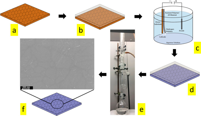
The sacrificial PMMA polymer support was removed from the PMMA/graphene/SiO2 composite via the newly developed Soxhlet extraction method. The apparatus, as shown in Figure 1, consists of a glass chamber equipped with a siphoning tube, vapor tube, and reflux condenser. The composite sample was carefully inserted into the extraction chamber using tweezers, and reagent-grade acetone was added into the flat bottom flask placed inside a heating mantle. The solvent was heated to achieve steady boiling of the solvent (>∼57 °C), allowing ultra-pure acetone to evaporate and subsequently condense and fill up the chamber containing the PMMA/graphene/SiO2 composite. The automated batch extraction process was allowed to continue for 4 h without any mechanical disturbance, after which the 2D material was removed from thimble, dried in a stream of N2 gas, and then stored in an air-tight sample holder. For comparison purposes, a conventional purification/annealing process20 was also carried out. Typically, the substrate containing the PMMA/graphene scaffold was thermally annealed to enhance the adherence of the scaffold onto the SiO2 substrate and then placed in acetone at room temperature for 2 h to remove the PMMA layer. The substrate was then rinsed with isopropyl alcohol (HPLC grade; Sigma-Aldrich, U.S.A; 99.9%) and dried with N2 gas (99.99% purity).
Figure 1.
Schematic diagram of Soxhlet-assisted graphene transfer. (a) Graphene on Cu foil, (b) graphene spin-coated with PMMA, (c) Cu foil removal by the electrochemical method and subsequent transfer on the SiO2/Si substrate, (d) graphene attached on the SiO2/Si-PMMA composite, (e) Soxhlet apparatus setup for PMMA removal, and (f) ultra-clean graphene on the target substrate.
Characterization
Raman spectra and point-by-point mapping were obtained with a HORIBA XploRa Raman Confocal system with an objective of 100X. The laser excitation wavelength was 532 nm, and a 1200 L mm–1 diffraction grating was used. A total of 2000 data points were collected on the transferred samples. The morphologies were analyzed using scanning electron microscopy (Zeiss Auriga FIB/FESEM) with an acceleration voltage of 5 kV and a working distance of 5 mm. AFM measurements were performed with an Oxford Research AFM (MFP-3D infinity) instrument using the tapping mode under ambient conditions, and Si tips coated with Al (TAP300AL-G probe, Budget Sensors) were used.
Soxhlet-Assisted Transfer onto Target Substrate
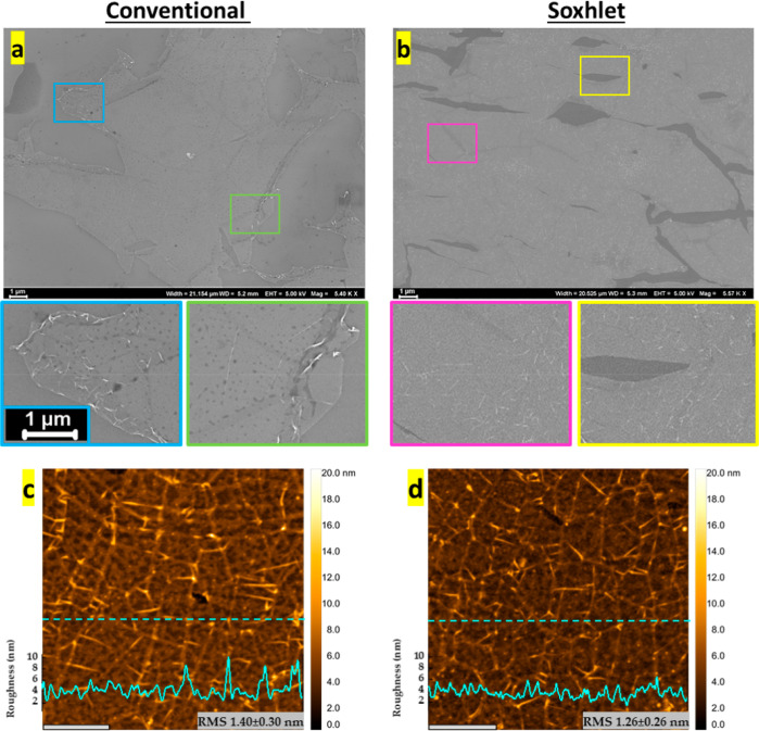
Our approach involves the use of Soxhlet apparatus as the key tool for benign PMMA removal in the graphene transfer process, including in situ preparation of ultra-pure acetone for dissolving the polymer (see the Supporting Information Video). In most transfer procedures, the polymer-removal step is carried out by mechanically agitating the sample in a solvent directly received from a commercial supplier, which subjects the sample to excessive handling, impurities inevitably present in the solvent, and dust from the atmosphere. Therefore, contaminants in the solvent sometimes leave residues in addition to those resulting from incomplete PMMA removal (see SEM images in Figure 2a,b). The Soxhlet provides a quick solution to all the above-mentioned problems. Thus, the polymer removal is performed in an enclosed chamber, minimizing exposure to dust. Mechanical agitation of the sample is negligible, with solvent condensing around the sample in a very gentle fashion. The solvent is continuously purified by distillation during the process, without the need for a separate distillation setup, and minimizing solvent consumption. Most importantly, repeated washing of the sample with the freshly distilled solvent allows for essentially complete removal of the polymer from the graphene surface. Other advantages offered by our Soxhlet-assisted polymer-removal procedure include eliminating the need for a clean room to carry out pristine transfer processes and repeated recycling of the same batch of the solvent in a green “closed loop” setup.
Figure 2.
Characterization of transferred graphene films on SiO2/Si substrates. SEM images of (a) conventional transfer method. (b) Soxhlet transfer method. Color framed insets represent zoomed areas. The AFM profile of (c) conventional transfer method. (d) Soxhlet transfer method, scale bare is 1 μm. Inset: The AFM line profile graph for both transfer techniques.
Characterization of Graphene Transferred by both Techniques
The quality of the transfer was initially confirmed using optical microscopy (see Supporting Information Figure S1). A quick surface scan of graphene films obtained by both Soxhlet-assisted and conventional transfer techniques showed substantial coverage of the substrate by graphene. Intermittent cracks attributed to the damaging effect of PMMA during removal21,22 were observed with both techniques but appeared less pronounced in the Soxhlet-assisted method. It was also observed that the rough surface of the Cu growth substrate left a distinctive pattern on the final graphene sheet transferred onto SiO2/Si. The as-transferred graphene was subsequently analyzed by SEM (Figure 2a,b and insets), providing additional information at the nanoscale level.
Impurities introduced by acetone are clearly seen as dark dots in magnified areas of Figure 2a (conventional) but not in Figure 2b (Soxhlet). Residual PMMA contamination is evidenced by the presence of charged features in the SEM images, particularly only around the edges of the graphene sheet, and is more pronounced with the conventional protocol, thus suggesting less efficient polymer removal compared to the Soxhlet procedure. Furthermore, the presence of PMMA oligomer residues tends to mask the distribution of grain boundary defects induced during CVD growth on Cu, as seen in Figure 2a. In contrast, the surface morphology of graphene obtained by the Soxhlet method clearly revealed the grain boundary defects, apparently due to more effective PMMA removal by this novel approach (Figure 2b). More so, minimal mechanical damage was detected with the Soxhlet method, which is in contrast with the conventional immersion washing approach where significant folding and cracking were observed in the final graphene film.
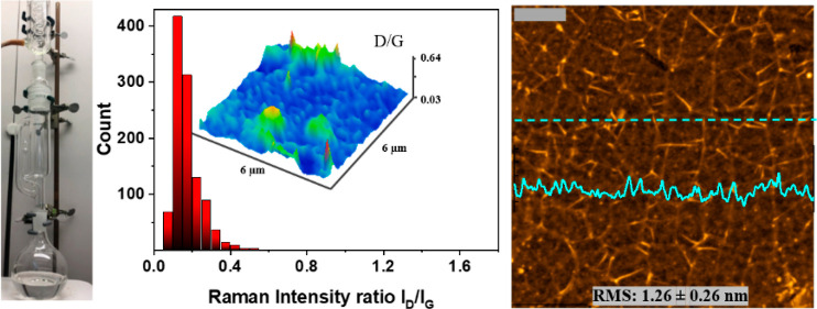
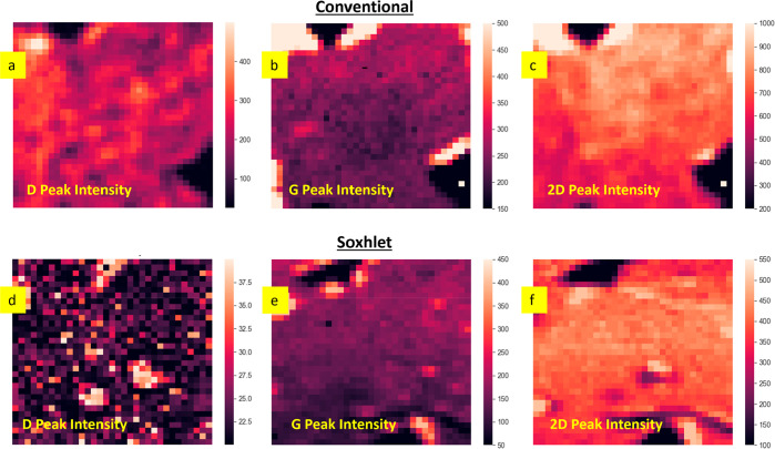
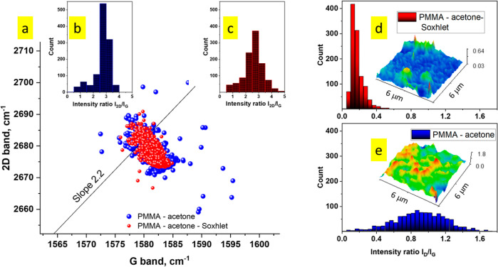
We further assessed the surface topology of the graphene films transferred with both techniques using AFM (Figure 2c,d). Imaging graphene areas of about 4 × 4 μm2, we observed less polymer contamination on the graphene film obtained by the Soxhlet method, as evidenced by the AFM line profile and the lower surface roughness root mean square value. We hypothesize that the improved efficiency of the PMMA removal in the Soxhlet-assisted transfer stems from nearly continuous contact of the PMMA–graphene/SiO2 substrate with freshly distilled acetone, effectively disrupting well-known strong interactions between PMMA and graphene.1,23,24 Additional evidence for the importance of a gentle yet rigorous polymer-removal procedure was obtained by micro-Raman spectroscopy, which was used to characterize graphene samples transferred either by Soxhlet or conventional methods (Figure 3a–f, also see Supporting Information Figure 2). Raman spectroscopy is a reliable technique to probe structural and electronic properties of graphene. An initial large-area scan in either the X- or Y-direction revealed a significantly greater number of defects/imperfections in graphene transferred by the conventional method. In contrast, the D-band was almost non-existent in the spectra of samples transferred using our Soxhlet method (see Supporting Information Figure S3). Defects in graphene originate either during the CVD growth25 or transfer1 processes, but it is noteworthy that both transfer processes were handled strictly identically prior to the PMMA-removal step, indicating that our novel transfer approach introduces fewer perturbations into the graphene film, leading to improved electronic and optical properties. Raman spectroscopy data are commonly used to evaluate the degree of doping and strain in graphene samples.26,27 Raman maps showed consistent results (Figure 3) for both techniques: the G and 2D bands of graphene appeared to be strong and homogeneous with the 2D peak full width half maximum of 32.4 cm–1 over the whole area of characterization (see Supporting Information Figure S4) and typical 2D/G intensity ratios for monolayer graphene (Figure 4b,c, Supporting Information Figure S5). The amount of introduced strain and doping is very similar for both techniques, as can be seen from the correlation plot on Figure 4a. In contrast, one might observe that the D-band peak is more pronounced in samples prepared by the conventional graphene transfer method, which is evidenced by the calculated D/G ratios plotted in Figure 4d,e and Supporting Information Figure S5. Here, the graphene film obtained by the Soxhlet method features a very weak D band, with the average D/G intensity ratio of only 0.17 ± 0.07 (Figure 4d). This indicates that the amount of defects introduced by the transfer technique is negligible. In contrast, the average D/G intensity ratio for the sample transferred using the conventional protocol is 0.90 ± 0.30 (Figure 4e), clearly indicating the presence of defects.
Figure 3.
Corresponding maps of plotted results of Raman characterization (10 × 10 μm2) of graphene transferred with (a–c) conventional PMMA method and (d–f) Soxhlet-assisted PMMA method.
Figure 4.
(a) Correlation map of the Raman G and 2D peak positions of graphene transferred with the conventional PMMA technique (blue) and Soxhlet-assisted PMMA technique (red). (b,c) Histogram of the 2D/G ratio with the same color code indicating the sample quality in general. (d,e) Histogram of the D/G ratio with the same color code as a signature of the defect amount. Insets show lateral distribution of the D/G ratio.
Repeated application of the proposed approach demonstrated high reproducibility, with expected minor sample to sample variations observed during the structural characterization (see Supporting Information Figure S2). The Soxhlet-assisted protocol has become the method of choice in our laboratory, allowing for multiple transfers to be conducted simultaneously, saving time and reagents, while preserving the quality and unique properties of graphene. A slight downside of our process is its energy intensive nature, and this is compensated by the conservation of the organic solvent (acetone) used in process purification and thus improving the carbon efficiency “cradle-to-cradle” of our process. The ability to process multiple samples at a time would further enhance the techno-economic feasibility of the Soxhlet-assisted protocol.
In conclusion, our Soxhlet-assisted method enabled transfer of a graphene film onto a target substrate with minimal surface contamination and damage associated with the conventional transfer process. The graphene film transferred by our new method shows fewer defects, as indicated by a substantially lower average D/G intensity ratio compared to the sample obtained by the conventional method. Although the amount of strain and doping appears similar in both techniques, less structural damage and more extensive polymer removal in the Soxhlet method could deliver materials of superior electrical, optical, and mechanical properties. Additionally, our new approach features experimental simplicity and reduced solvent use, potentially permitting the use of more affordable solvents of a lower degree of purification. Furthermore, this procedure can be applied for transfer of other delicate two-dimensional materials.
Acknowledgments
The work was performed at the Joint School of Nanoscience and Nanoengineering (JSNN), a member of the Southeastern Nanotechnology Infrastructure Corridor (SENIC) and the National Nanotechnology Coordinated Infrastructure (NNCI), which is supported by the National Science Foundation (Grant ECCS-1542174). Some graphene samples for this publication were provided by The Pennsylvania State University Two-Dimensional Crystal Consortium—Materials Innovation Platform (2DCC-MIP), which is supported by NSF cooperative agreement DMR-1539916.
Supporting Information Available
The Supporting Information is available free of charge at https://pubs.acs.org/doi/10.1021/acsomega.1c07113.
Author Contributions
Conceptualization, O.O.A., A.P., and T.I.; Experimental, O.O.A., S.P., A.T., and T.I.; Writing—original draft preparation, O.O.A., S.P., and T.I.; Writing—review and editing, O.O.A., A.P., and T.I. All authors have read and agreed to the published version of the article.
This research was funded by the NSF RAPID grant (CHE-2032601) (T.I.) and AFOSR grant 21RT0654 (A.P.).
The authors declare no competing financial interest.
Supplementary Material
References
- Leong W. S.; Wang H.; Yeo J.; Martin-Martinez F. J.; Zubair A.; Shen P.-C.; Mao Y.; Palacios T.; Buehler M. J.; Hong J.-Y.; Kong J. Paraffin-Enabled Graphene Transfer. Nat. Commun. 2019, 10, 867. 10.1038/s41467-019-08813-x. [DOI] [PMC free article] [PubMed] [Google Scholar]
- Chen Y.; Gong X. L.; Gai J. G. Progress and Challenges in Transfer of Large-Area Graphene Films. Adv. Sci. 2016, 3, 1500343. 10.1002/advs.201500343. [DOI] [PMC free article] [PubMed] [Google Scholar]
- Lin L.; Zhang J.; Su H.; Li J.; Sun L.; Wang Z.; Xu F.; Liu C.; Lopatin S.; Zhu Y.; Jia K.; Chen S.; Rui D.; Sun J.; Xue R.; Gao P.; Kang N.; Han Y.; Xu H. Q.; Cao Y.; Novoselov K. S.; Tian Z.; Ren B.; Peng H.; Liu Z. Towards Super-Clean Graphene. Nat. Commun. 2019, 10, 1912. 10.1038/s41467-019-09565-4. [DOI] [PMC free article] [PubMed] [Google Scholar]
- Xu S.; Zhang L.; Wang B.; Ruoff R. S. Chemical Vapor Deposition of Graphene on Thin-Metal Films. Cell Rep. Phys. Sci. 2021, 2, 100372. 10.1016/j.xcrp.2021.100372. [DOI] [Google Scholar]
- Shivayogimath A.; Whelan P. R.; MacKenzie D. M. A.; Luo B.; Huang D.; Luo D.; Wang M.; Gammelgaard L.; Shi H.; Ruoff R. S.; Bøggild P.; Booth T. J. Do-It-Yourself Transfer of Large-Area Graphene Using an Office Laminator and Water. Chem. Mater. 2019, 31, 2328–2336. 10.1021/acs.chemmater.8b04196. [DOI] [Google Scholar]
- Johnson B. Y.; Liu X.; Mazumder P.; Soni K. K.. Transfer of Monolayer Graphene onto Flexible Glass Substrates. WO 2016106039 A1, June 30, 2016.
- Kumar S.; Kaushik S.; Pratap R.; Raghavan S. Graphene on Paper: A Simple, Low-Cost Chemical Sensing Platform. ACS Appl. Mater. Interfaces 2015, 7, 2189–2194. 10.1021/am5084122. [DOI] [PubMed] [Google Scholar]
- Marchena M.; Wagner F.; Arliguie T.; Zhu B.; Johnson B.; Fernández M.; Chen T. L.; Chang T.; Lee R.; Pruneri V.; Mazumder P. Dry Transfer of Graphene to Dielectrics and Flexible Substrates Using Polyimide as a Transparent and Stable Intermediate Layer. 2D Mater. 2018, 5, 035022. 10.1088/2053-1583/aac12d. [DOI] [Google Scholar]
- Wood J. D.; Doidge G. P.; Carrion E. A.; Koepke J. C.; Kaitz J. A.; Datye I.; Behnam A.; Hewaparakrama J.; Aruin B.; Chen Y.; Dong H.; Haasch R. T.; Lyding J. W.; Pop E. Annealing Free, Clean Graphene Transfer Using Alternative Polymer Scaffolds. Nanotechnology 2015, 26, 055302. 10.1088/0957-4484/26/5/055302. [DOI] [PubMed] [Google Scholar]
- Van Ngoc H.; Qian Y.; Han S. K.; Kang D. J. PMMA-Etching-Free Transfer of Wafer-Scale Chemical Vapor Deposition Two-Dimensional Atomic Crystal by a Water Soluble Polyvinyl Alcohol Polymer Method. Sci. Rep. 2016, 6, 33096. 10.1038/srep33096. [DOI] [PMC free article] [PubMed] [Google Scholar]
- Marta B.; Leordean C.; Istvan T.; Botiz I.; Astilean S. Efficient Etching-Free Transfer of High Quality, Large-Area CVD Grown Graphene onto Polyvinyl Alcohol Films. Appl. Surf. Sci. 2016, 363, 613–618. 10.1016/j.apsusc.2015.11.265. [DOI] [Google Scholar]
- Kang M. H.; Prieto López L. O.; Chen B.; Teo K.; Williams J. A.; Milne W. I.; Cole M. T. Mechanical Robustness of Graphene on Flexible Transparent Substrates. ACS Appl. Mater. Interfaces 2016, 8, 22506–22515. 10.1021/acsami.6b06557. [DOI] [PubMed] [Google Scholar]
- Jensen W. B. The Origin of the Soxhlet Extractor. J. Chem. Educ. 2007, 84, 1913. 10.1021/ed084p1913. [DOI] [Google Scholar]
- Mussatto S. I.Chapter 11 - Generating Biomedical Polyphenolic Compounds from Spent Coffee or Silverskin. In Coffee in Health and Disease Prevention; Preedy V. R., Ed.; Academic Press: San Diego, 2015; pp 93–106. [Google Scholar]
- Misra K.; Sharma P.; Bhardwaj A.. Management of High Altitude Pathophysiology; Academic Press, 2018. [Google Scholar]
- Luque de Castro M. D.; García Ayuso L. E.. Environmental Applications|Soxhlet Extraction. In Encyclopedia of Separation Science; Elsevier, 2000; pp 2701–2709. [Google Scholar]
- Ikawa M.; Yamada T.; Matsui H.; Minemawari H.; Tsutsumi J. y.; Horii Y.; Chikamatsu M.; Azumi R.; Kumai R.; Hasegawa T. Simple Push Coating of Polymer Thin-Film Transistors. Nat. Commun. 2012, 3, 1176. 10.1038/ncomms2190. [DOI] [PMC free article] [PubMed] [Google Scholar]
- Woody K. B.; Palkar A.; Bullock J. E.. Method of Purifying Conjugated Polymers. U.S. Patent 9,045,596 B2, June 2, 2015.
- Oh K. S.; Oh J. H.; Kim Y. H.; Cho D. H.; Kim M. R.; YU S. M.; Lee J. K.. Preparation Method of Hydrophobic Silica Aerogel. U.S. Patent 20,160,264,427 A1, September 15, 2016.
- Park H.; Brown P. R.; Bulović V.; Kong J. Graphene As Transparent Conducting Electrodes in Organic Photovoltaics: Studies in Graphene Morphology, Hole Transporting Layers, and Counter Electrodes. Nano Lett. 2012, 12, 133–140. 10.1021/nl2029859. [DOI] [PubMed] [Google Scholar]
- Choi W.; Shehzad M. A.; Park S.; Seo Y. Influence of Removing PMMA Residues on Surface of CVD Graphene Using a Contact-Mode Atomic Force Microscope. RSC Adv. 2017, 7, 6943–6949. 10.1039/c6ra27436f. [DOI] [Google Scholar]
- Shahzad K.; Jia K.; Zhao C.; Yan X.; Yadong Z.; Usman M.; Luo J. An Improved Rosin Transfer Process for the Reduction of Residue Particles for Graphene. Nanoscale Res. Lett. 2020, 15, 85. 10.1186/s11671-020-03312-1. [DOI] [PMC free article] [PubMed] [Google Scholar]
- Zhang Z.; Du J.; Zhang D.; Sun H.; Yin L.; Ma L.; Chen J.; Ma D.; Cheng H.-M.; Ren W. Rosin-Enabled Ultraclean and Damage-Free Transfer of Graphene for Large-Area Flexible Organic Light-Emitting Diodes. Nat. Commun. 2017, 8, 14560. 10.1038/ncomms14560. [DOI] [PMC free article] [PubMed] [Google Scholar]
- Nasir T.; Kim B. J.; Hassnain M.; Lee S. H.; Jeong B. J.; Choi I. J.; Kim Y.; Yu H. K.; Choi J.-Y. Plasticized Polystyrene by Addition of -Diene Based Molecules for Defect-Less CVD Graphene Transfer. Polymers 2020, 12, 1839. 10.3390/polym12081839. [DOI] [PMC free article] [PubMed] [Google Scholar]
- Chin H.-T.; Lee J.-J.; Hofmann M.; Hsieh Y.-P. Impact of Growth Rate on Graphene Lattice-Defect Formation within a Single Crystalline Domain. Sci. Rep. 2018, 8, 4046. 10.1038/s41598-018-22512-5. [DOI] [PMC free article] [PubMed] [Google Scholar]
- Bendiab N.; Renard J.; Schwarz C.; Reserbat-Plantey A.; Djevahirdjian L.; Bouchiat V.; Coraux J.; Marty L. Unravelling External Perturbation Effects on the Optical Phonon Response of Graphene: External Perturbation Effects on Graphene Optical Phonons. J. Raman Spectrosc. 2018, 49, 130–145. 10.1002/jrs.5267. [DOI] [Google Scholar]
- Mueller N. S.; Heeg S.; Alvarez M. P.; Kusch P.; Wasserroth S.; Clark N.; Schedin F.; Parthenios J.; Papagelis K.; Galiotis C.; Kalbáč M.; Vijayaraghavan A.; Huebner U.; Gorbachev R.; Frank O.; Reich S. Evaluating Arbitrary Strain Configurations and Doping in Graphene with Raman Spectroscopy. 2D Mater. 2017, 5, 015016. 10.1088/2053-1583/aa90b3. [DOI] [Google Scholar]
Associated Data
This section collects any data citations, data availability statements, or supplementary materials included in this article.


