Abstract
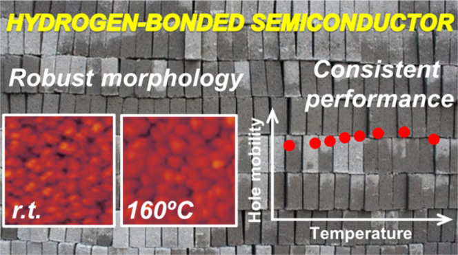
Molecular organization plays an essential role in organic semiconductors since it determines the extent of intermolecular interactions that govern the charge transport present in all electronic applications. The benefits of hydrogen bond-directed self-assembly on charge transport properties are demonstrated by comparing two analogous pyrrole-based, fused heptacyclic molecules. The rationally designed synthesis of these materials allows for inducing or preventing hydrogen bonding. Strategically located hydrogen bond donor and acceptor sites control the solid-state arrangement, favoring the supramolecular expansion of the π-conjugated surface and the subsequent π-stacking as proved by X-ray diffraction and computational calculations. The consistency observed for the performance of organic field-effect transistors and the morphology of the organic thin films corroborate that higher stability and thermal robustness are achieved in the hydrogen-bonded material.
Keywords: hydrogen-bonded materials, self-assembly, organic semiconductors, hole-transporting materials, organic electronics, charge transport, organic field-effect transistors
Introduction
Organic semiconductors have gained much interest due to their application in the areas of electronics and photonics for the fabrication of a new generation of optoelectronic devices such as organic light-emitting diodes (OLEDs), organic field-effect transistors (OFETs), or organic and hybrid solar cells, among other products related to electronic applications.1−4 The technical properties of this new generation of devices (flexibility, lightweight, and reduced cost) make them very appealing for the electronics industry. Nevertheless, although devices such as OLEDs have already reached the stage of commercial exploitation,5 some issues mainly related to the stability, durability, and efficiency of organic materials, and devices based on these types of materials, still need to be solved so that organic electronics can truly represent a profitable alternative.6
An important part of the typical limitations of organic semiconductors comes from their nature as molecular solids. The solid-state arrangement of these materials is mainly governed by weak noncovalent intermolecular interactions, which is the reason why organic semiconductors are commonly considered as disordered solids.7,8 As a consequence, wide electronic band structures, comparable to those found for inorganic semiconductors, are not generally achieved, and bandlike transport is rather uncommon in organic semiconductors.9,10 This has been observed in highly pure crystals at low temperatures where molecular vibrations are to a large extent quenched.11−14 Nevertheless, charge transport in disordered organic thin films at room temperature becomes more difficult15,16 because it has to follow a thermally activated hopping mechanism within a manifold of localized states.17−19 These localized states are associated with the frontier molecular orbitals of the organic semiconductor, whose topology and overlap between neighboring molecules determine the charge transport.20 As such, the molecular organization in the solid state strongly affects charge mobility and thus electrical performance.21,22 Given the π-conjugated structure of organic semiconductors, the connection between molecules is mainly due to π–π interactions that, according to the relative orientation of the interacting molecules, could be basically classified as either face-to-face or edge-to-face.23 Despite the indispensable contribution of these π–π interactions to charge carrier hopping, especially in the case of face-to-face stacking, it is difficult to adjust their direction with the aim of gaining some control on the molecular organization in the solid state.24 Hence, the cooperative effect of stronger noncovalent interactions could enable better control over the disposition of π-conjugated molecules. In this regard, hydrogen bonding is particularly helpful.25,26 The large variety of functional groups and building blocks that can work as hydrogen bond donor or hydrogen bond acceptor units becomes a synthetic resource that opens up the possibility of preparing an enormous diversity of molecules. Additionally, the high energy of hydrogen bonds, from the perspective of noncovalent interactions, as well as their directionality, would result in more stable materials where the orientation of the molecules could be better predicted. This strategy based on hydrogen bond-directed self-assembly has been widely used to control the molecular arrangement in the solid state, and also in solution, through the discipline of crystal engineering, representing one of the most important tools for the development of supramolecular chemistry.27−30 Moreover, the macromolecular organization through hydrogen bond interactions is ubiquitous in biological systems.31
In agreement with these premises, the approach based on molecular self-assembly could also contribute to the development of novel semiconducting materials and the progress of organic electronics. Although this methodology has been explored for some conjugated materials, the synthetic strategy often turns to the peripheral functionalization of the conjugated system with hydrogen bonding functions and solubilizing groups.31−33 However, the bulkiness and insulating character of the attached substituents could interfere with the charge transport process. Only recently, conjugated systems integrating hydrogen bond donor and acceptor sites within the conjugated structure have been reported. In this context, it is worth highlighting the excellent results obtained for different studies of quinacridone and epindolidione leading to high hole mobilities in thin-film OFETs, even showing ambipolar charge transport by means of interfacial engineering.34 Analogously, the building block of indolinone admits different isomer structures whose hydrogen bonding properties can be exploited in the field of organic electronics. This is the case of the studies reported for indigo and diketopyrrolopyrroles.35−37 Additionally, an elegant tuning of the molecular arrangement via hydrogen bonding was achieved through the perchlorination of perylenediimide, which reached quite remarkable electron mobility upon controlling the substrate temperature during the OFET fabrication.38 All of these examples have in common the use of N–H groups as hydrogen bond donors and carbonyl groups as hydrogen bond acceptors. Some other structural motifs that have been reported to form hydrogen-bonded frameworks in organic semiconductors include pentacene and hexacene quinones (C–H···O=C),39 dichloropentacene (C–H···Cl),40 dihydrotetraazapentacenes (N–H···N),41 and pyrrolobenzothiazines (N–H···N, C–H···N).42
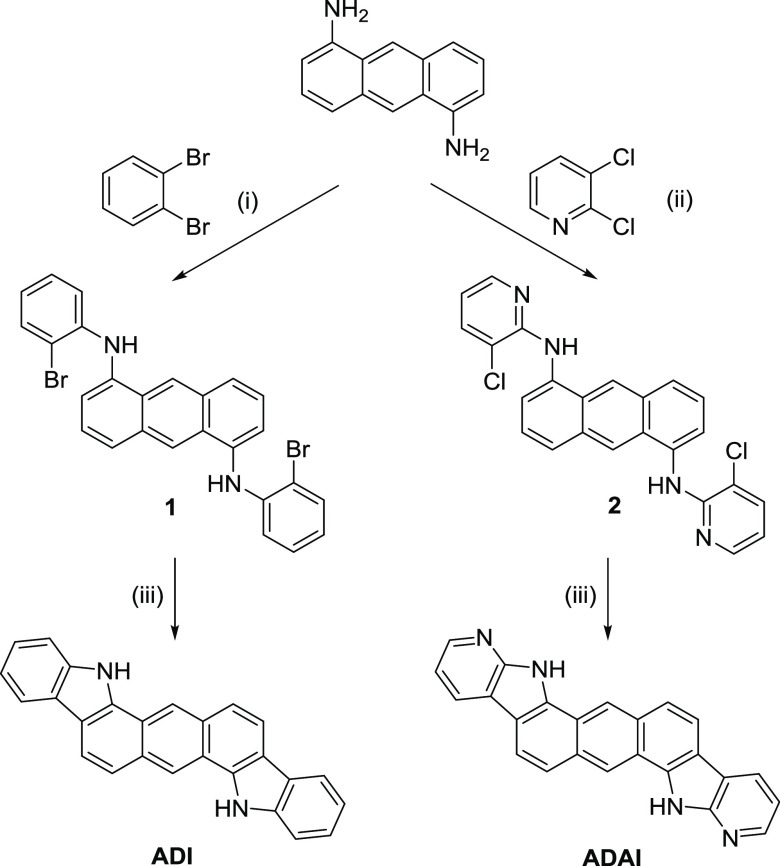
Recently, we have reported the synthesis of a series of molecules where the integration of the 7-azaindole substructure into a fused polyheteroaromatic system results in a hydrogen bond-directed self-assembly (N–Hpyrrole···Npyridine).43,44 Interestingly, this type of structure does not compromise the conjugation throughout the whole fused polycyclic molecule, allowing for better charge delocalization. We hypothesized with the possibility that, upon self-assembly, the supramolecular adduct would present an extended π-surface that subsequently would improve the intermolecular π–π interactions. Based on this hypothesis, the increase of the conjugation length in the molecule to self-assemble should further benefit the intermolecular interactions. Thus, we present a comparative study between two heptacyclic compounds, namely, 7,15-dihydroanthra[1,2-b:5,6-b′]diindole, ADI, and 7,15-dihydroanthra[1,2-b:5,6-b′]di(7-azaindole), ADAI (Scheme 1). The benzene or pyridine rings located at the extremes of each molecule (ADI or ADAI) make a critical difference that, respectively, prevents or enables the intermolecular interactions by hydrogen bonding (N–Hpyrrole···Npyridine). As a consequence, noticeable differences are observed in the solid-state packing. This affects the thin-film morphology and hole mobility, as further evidenced by observing the evolution upon thermal annealing of the thin-film transistors fabricated with the reported materials. The significant robustness observed for the self-assembled material based on ADAI demonstrates the suitability of our self-assembly strategy for the design of π-conjugated systems, conferring high stability to the organic thin films and the corresponding electronic devices.
Scheme 1. Synthetic Routes for ADI and ADAI.
(i) (±)-2,2′-Bis(diphenylphosphino)-1,1′-binaphthalene (BINAP), Pd(dba)2, K2CO3, toluene, reflux (37%); (ii) (±)-BINAP, Pd(OAc)2, tBuOK, 1,4-dioxane, reflux (68%); and (iii) dimethyl sulfoxide (DMSO), tBuOK, hν (ADI: 67%; ADAI: 96%).
Experimental Section
General
Commercially available reagents and solvents were used for the synthesis, purification, and characterization of the reported compounds without any additional purification unless stated otherwise. ADI and ADAI were obtained with high purity by purification via gradient sublimation (pressure < 10–6 mbar). 1H NMR and 13C NMR spectra were acquired on a Bruker AV200, Bruker AV300, or Bruker AV400 spectrometer. The residual solvent peaks were used as a reference for the chemical shifts, which are given in ppm. Mass spectra were measured on a high-performance liquid chromatography-mass spectrometry (HPLC-MS) time-of-flight (TOF) 6220 instrument. Noncorrected melting points were measured using a Reichert instrument. An SDT 2960 analyzer from TA Instruments was employed for thermogravimetric analysis (TGA) under an inert atmosphere (heating rate: 10 °C min–1). Ultraviolet–visible (UV–vis) spectra were acquired on a Cary 5000 spectrophotometer using dimethylformamide (DMF) solutions. Cyclic voltammetry experiments were performed in DMF using a BAS potentiostat. A boron-doped diamond was used as the working electrode, Pt wire was used as the counter electrode, Ag/AgCl as the reference electrode, and the ferrocene/ferrocenium (Fc/Fc+) couple as the internal reference. The scan rate was 100 mV s–1. Tetrabutylammonium hexafluorophosphate (0.1 M) was the supporting electrolyte.
Synthetic Methods
Compound 2 and ADAI were synthesized following previously reported synthetic procedures.44
N,N′-Bis(2-bromophenyl)anthracene-1,5-diamine, 1
(±)-2,2′-Bis(diphenylphosphino)-1,1′-binaphthalene (BINAP) (0.22 g, 7.5 mol%) was suspended in distilled toluene (30 mL) in a two-neck round-bottom flask under a nitrogen atmosphere. The mixture was heated in an oil bath until it was completely dissolved. Then, bis(dibenzylideneacetone)palladium(0) (Pd(dba)2) (0.14 g, 5.0 mol%) was added, and the resulting solution was stirred for 15 min. In another two-neck round-bottom flask under an inert atmosphere, 1,5-diaminoanthracene (1.00 g, 4.80 mmol), 1,2-dibromobenzene (1.74 mL, 14.4 mmol), and potassium carbonate (3.98 g, 28.8 mmol) were placed with 30 mL of distilled toluene. The catalyst was transferred via a syringe to the reaction flask and it was heated at the reflux temperature. The reaction evolution was followed using thin layer chromatography. Finally, the crude was cooled to room temperature, and the solvent was removed under reduced pressure. The resulting crude was washed with water (3 × 30 mL) and triturated with diethyl ether (3 × 30 mL) to obtain the N-arylated compound (1.86 g, 37%). Mp.: 233–234 °C. 1H NMR (400 MHz, CDCl3), δ: 8.64 (s, 2H), 7.84 (dd, J = 6.4, 3.2 Hz, 2H), 7.60 (dd, J = 8.4, 1.6 Hz, 2H), 7.43 (t, J = 6.4 Hz, 2H), 7.43 (d, J = 3.2 Hz, 2H), 7.10 (td, J = 8.4, 1.2 Hz, 2H), 6.96 (dd, J = 8.4, 1.2 Hz, 2H), 6.75 (td, J = 8.4, 1.6 Hz, 2H), 6.52 (s, 2H, NH) ppm. 13C NMR (50.3 MHz, CDCl3), δ: 142.9, 137.3, 132.8, 132.7, 128.2, 128.0, 125.5, 125.4, 121.7, 120.5, 118.1, 116.1, 111.6 ppm. HRMS (ESI) m/z: [M + H]+ Calcd. for C26H19Br2N2: 516.991; Found: 516.9901.
7,15-Dihydroanthra[1,2-b:5,6-b′]diindole, ADI
To a photochemical reactor containing anhydrous dimethyl sulfoxide (160 mL) under a continuous nitrogen flow, potassium tert-butoxide (1.34 g, 11.9 mmol) and N,N′-bis(2-bromophenyl)anthracene-1,5-diamine (1.41 g, 2.72 mmol) were sequentially added. The resulting mixture was degassed for 15 min before being irradiated with a medium-pressure mercury lamp for 2.0 h. Afterward, the crude was allowed to reach room temperature and poured into a saturated solution of ammonium chloride (50 mL). The resulting precipitate was filtered under vacuum, washed with water (3 × 30 mL) and methanol (3 × 30 mL) to isolate the desired product (0.65 g, 67%). Mp: > 300 °C. 1H NMR (300 MHz, DMSO-d6), δ: 12.49 (s, 2H, NH), 9.21 (s, 2H), 8.26 (d, J = 8.7 Hz, 2H), 8.19 (d, J = 7.7 Hz, 2H), 7.82 (d, J = 8.7 Hz, 2H), 7.69 (d, J = 7.7 Hz, 2H), 7.41 (t, J = 7.7 Hz, 2H), 7.41 (t, J = 7.7 Hz, 2H) ppm. 13C NMR (101 MHz, DMSO-d6), δ: 138.9, 135.4, 130.5, 124.6, 124.0, 121.2, 120.7, 120.4, 119.9, 119.9, 119.8, 116.3, 112.0 ppm. HRMS (ESI) m/z: [M + H]+ Calcd. for C26H17N2: 355.1241; Found: 355.1251.
OFET Fabrication and Characterization
Thin-film OFETs were fabricated with a bottom-gate top-contact configuration. P-doped n++ silicon wafers coated with a 300 nm thick layer of thermally grown SiO2 were used. The cleaning protocol of the substrates consisted of sequential sonication with water, acetone, and isopropanol for 20 min. Next, a self-assembled monolayer of octadecyltrimethoxysilane (OTS) was grown on the surface of SiO2 following a reported protocol.45 Then, 50 nm thick films of ADI and ADAI were thermally evaporated under high vacuum conditions (1 × 10⁻⁷ mbar) onto the OTS-coated substrates at a rate of 0.2 Å s–1. The device structures were completed by the sequential evaporation of 8 nm of MoO3 (rate: 0.1 Å s–1) and 25 nm of Au (rate: 0.2 Å s–1) through a shadow mask. The OFET channel dimensions were 2 mm width and 40–140 μm length confirmed by profilometry. A Keithley 2636A semiconductor parameter analyzer was used to measure the current–voltage (I–V) curves at room temperature under an ambient atmosphere. The field-effect mobility was extracted in the saturation regime. Before each measurement, the device was annealed in a hot plate at the indicated temperature for 15 min and cooled to room temperature.
Morphology
Tapping mode atomic force microscopy (AFM) images were recorded using an NT-MDT microscope (NTEGRA PRIMA) and analyzed with Gwyddion V2.47.
X-ray Diffraction (XRD)
The single-crystal X-ray data were collected at 100 K with a Bruker D8Quest Kappa diffractometer using Cu Kα radiation. The structure was solved using direct methods and refined on F2 by the full-matrix least-squares method, using SHELX-2018 software package and expanded using Fourier techniques. All nonhydrogen atoms were refined anisotropically. The H atom bonded to the nitrogen atom was located in a difference Fourier map and refined freely. Other hydrogen atoms were included in geometrically calculated positions and were refined according to the riding model. CCDC deposition numbers: ADI (2036011) and ADAI (1957368).
X-ray diffraction diffractograms of the material deposited as a thin film were collected on a Bruker D8 Advance instrument using θ–θ mode with Cu Kα radiation (wavelength 1.54060 Å), 40 kV, 30 mA, and a one-dimensional detector with a window of 1°. Primary optics consisted of a 2° Soller slit, a 1 mm incidence slit, and an air scatter screen. Secondary optics included a 3 mm antiscatter slit, a Ni filter, and a 2.5° Soller slit. The sample was step-scanned from 3 to 65° in 2θ, with 0.05° stepping intervals, 1 s per step, and a rotation speed of 30 rpm.
Computational Methods
All DFT calculations were carried out within the Gaussian 16 (revision A.03) software package46 using the B3LYP-D3BJ47−49 functional together with the 6-31G** basis set.50Ci-symmetry constraints were applied during the geometry optimizations of the neutral and radical cation species to evaluate the internal reorganization energies. Solvent effects were described using the polarized continuum model (PCM) approach.51 Transfer integrals tij were calculated within the DIPRO approximation52 implemented in a homemade program. See the Supporting Information for a full description of the calculation of the charge transport properties.
Results and Discussion
Synthesis and Characterization
The synthesis of ADI and ADAI was accomplished by a straightforward methodology of two steps only (Scheme 1), which represents an important advantage for the simplification of material production. Initially, 1,5-diaminoanthracene53 is reacted with the corresponding dihaloarene to obtain the palladium-catalyzed C–N coupling via a Buchwald–Hartwig reaction.54 In the case of ADI, o-dibromobenzene was employed. Analogously, 2,3-dichloropyridine was used for the synthesis of ADAI. As expected, the latter reacted with high selectivity through position 2 of the pyridine ring to obtain the desired product. The second step consisted of double intramolecular C–C coupling photochemically achieved through a radical aromatic substitution. This synthetic route led to higher yields in the case of the reactions carried out with pyridine than those corresponding to the benzene-ended products.
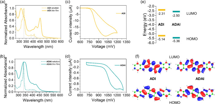
The electronic properties of the molecular systems were investigated using absorption spectroscopy and cyclic voltammetry. The similarities between both conjugated compounds, ADI and ADAI, are displayed in the UV–vis spectra (Figure 1a,b) showing the more intense band at 334 and 337 nm, respectively, in dimethylformamide (DMF) solution. Moreover, less intense absorption, ascribed to the α and p bands of the polyheteroaromatic skeleton,55 is observed at lower energies, with the spectra onset located at 437 nm (ADI) and 433 nm (ADAI). Regarding the characterization in the solid state, thin films were evaporated on quartz substrates. The absorption spectra experienced the expected red shift resulting from the intermolecular interactions that narrow the optical gap.
Figure 1.
Normalized absorption spectra of (a) ADI and (b) ADAI in DMF solution and as thin films deposited on quartz substrates. Cyclic voltammograms of (c) ADI and (d) ADAI. (e) Highest occupied molecular orbital (HOMO) and lowest unoccupied molecular orbital (LUMO) energy levels. (f) Topology of the calculated HOMO and LUMO frontier molecular orbitals.
Cyclic voltammograms displayed irreversible electrochemical processes for both ADI and ADAI compounds (Figure 1c,d), presumably due to poor stability of the radical cation formed after the oxidative scan. The anodic peak potentials (Ep-ADI = 973 mV; Ep-ADAI = 1176 mV) evidenced the effect of the more electron-deficient pyridine rings in ADAI when compared to those of ADI with benzene rings at both extremes of the molecule. Therefore, since the presence of pyridine makes the compound more difficult to be oxidized, a higher potential is measured for ADAI (Table 1). In agreement with this, its highest occupied molecular orbital (HOMO) becomes more stable than that determined for ADI (Figure 1e). Due to the impossibility of detecting the reduction potential of the studied molecules within the electrochemical window accessible under the employed experimental conditions, the energies of the lowest unoccupied molecular orbital (LUMO) were indirectly estimated by adding the previously measured optical gap to the HOMO energy. It is worth noticing that the low HOMO energies assessed for these compounds could improve their stability toward ambient conditions (atmospheric oxygen and moisture) that commonly cause degradation of electronic devices fabricated with organic materials.
Table 1. Optical and Electrochemical Characterization.
| λonseta (nm) | Eopt. (eV) | λonsetb (nm) | Eopt. (eV) | Eonset ox. (mV) | HOMOc (eV) | LUMOd (eV) | |
|---|---|---|---|---|---|---|---|
| ADI | 437 | 2.83 | 471 | 2.63 | 776 | –5.14 | –2.31 |
| ADAI | 433 | 2.86 | 463 | 2.68 | 1000 | –5.36 | –2.50 |
Spectra acquired in DMF solution.
Spectra for thin films.
EHOMO = −e(Eonset ox. – Eonset ox. Fc/Fc+) + EHOMO Fc (Fc stands for ferrocene; Eonset ox. Fc/Fc+ = 0.44 V; EHOMO Fc = −4.8 eV).
ELUMO = EHOMO + Eopt.
To obtain further insight into the electronic structures of the ADI and ADAI systems, density functional theory (DFT) calculations were performed at the B3LYP/6-31G** level in the presence of DMF. Figure 1f displays the topology of the calculated HOMO and LUMO levels. In both cases, the molecular orbitals, although showing a larger contribution from the central anthracene unit, are spread all over the conjugated backbone, which should favor the intramolecular charge delocalization and the intermolecular electronic communication. In terms of energetics, DFT calculations predict an energy stabilization of both HOMO and LUMO levels when passing from ADI (−4.95 and −1.60 eV, respectively) to ADAI (−5.12 and −1.79 eV). The relative energy shifts of the HOMO and LUMO levels between both systems are in line with the experimental estimates, highlighting that ADI exhibits a slightly larger electron-donor character compared to ADAI.
The thermal stabilities of ADI and ADAI were determined by thermogravimetric analysis (Figure S3) that revealed a degradation temperature (Tdeg. measured for a 5% mass loss) of 409 °C (ADI) and 496 °C (ADAI). Although both molecules are considered highly stable, the significant 87 °C difference observed between the Tdeg. values can be interpreted as evidence of the higher thermal robustness of ADAI. This is very likely due to the solid-state arrangement, stabilized by hydrogen bond interactions, as discussed below.
Solid-State Structure
As previously stated, the molecular organization of π-conjugated molecules plays a crucial role in the charge transport ability of organic semiconductors since it conditions the intermolecular orbital overlap that, in the end, directs the charge carrier hopping. X-ray diffraction (XRD) experiments corroborated the expected differences in the crystal packing of ADI and ADAI. The molecule that cannot self-assemble by hydrogen bonds, i.e., ADI, crystalizes in a monoclinic cell (space group P21/m). It shows a herringbone packing, very common in fused polyheteroaromatic systems with a similar structure (Figure 2a).56,57
Figure 2.
Molecules showing van der Waals contacts in the crystal packing of (a) ADI and (e) ADAI (color code: gray = carbon, purple = nitrogen, and white = hydrogen), (b) and (f) top view, (c) and (g) view across the short edge, and (d) and (h) view across the long edge of the molecules closely packed in parallel planes for ADI and ADAI, respectively.
Each molecule of ADI is in van der Waals contact with eight neighbor molecules establishing edge-to-face (C–H···π and N–H···π) and face-to-face interactions (π–π). Molecules packed in parallel planes commonly define the orientation where the better overlap is achieved. Nevertheless, a perfect overlap of π-conjugated systems is energetically disfavored due to the electrostatic repulsion between two confronted surfaces with identical electronic densities. Accordingly, fused polyaromatic molecules packed in parallel planes generally adopt a shifted disposition that is characterized by the pitch and roll angles, related to the intermolecular sliding along the long and short molecular edges, respectively.58 Taking the longer molecular axis as a reference, ADI (Figure 2c,d) shows a pitch angle of 39° and a roll angle of 66°, which, respectively, correspond to a short shift (1.9 Å) along the long edge and a rather long shift (5.4 Å) along the short edge. These shifts determine the intermolecular overlap (Figure 2b), which, in turn, might affect the charge transport.
Regarding the crystal structure of ADAI, it crystallizes in a triclinic cell (space group P 1̅). The crystal packing is characterized by a slipped-stacking where each molecule is in van der Waals contact with four neighboring molecules (Figure 2e), showing a higher density than that of the crystals of ADI. In this case, the centrosymmetric geometry of the molecules leads to a hydrogen bond-directed self-assembly (N–Hpyrrole···Npyridine) that results in a ribbonlike structure. This supramolecular organization contributes to the stabilization of a π-expanded surface. Consequently, these ribbons pile up forming a columnar arrangement or, in other words, the columnar arrangement is stabilized by the hydrogen bonds between adjacent columns (Figure 2e). The observed crystal structure proves our initial hypothesis and reinforces the relevance of hydrogen bonding as a useful tool for the molecular design and the subsequent control of the solid-state structure. ADAI molecules packed through π–π stacking display pitch and roll angles of 41° and 2°, respectively (Figure 2g,h). Accordingly, the ADAI molecules show short slippage along the long edge (2.9 Å) and short edge (0.1 Å) that is shown in the abovementioned columnar disposition.
Charge Transport in OFETs and Thin-Film Characterization
Charge transport properties of ADI and ADAI were characterized in OFETs with a bottom-gate top-contact architecture, fabricated, without substrate heating, on silicon substrates with a thermally grown silicon oxide layer that was covered with a self-assembled monolayer of OTS. The organic semiconductors were evaporated through a shadow mask, followed by the evaporation of a thin layer of molybdenum oxide and finally the gold contacts. The transfer and output characteristics are depicted in Figure 3. A perfectly linear current intensity–voltage (I–V) plot is observed at low source–drain voltages (VD) in the output characteristics, demonstrating the good ohmic contact between the semiconductor and the source–drain electrodes, as it was intended using the MoO3 interfacial layer. The high work function of MoO3 improves the charge injection on semiconductors with low-lying HOMOs such as ADI and ADAI.59 Mobilities were calculated in the saturated regime from the transfer characteristics measured in air. The ADI mobility (4 × 10⁻⁴ cm2 V–1 s–1) was more than 1 order of magnitude lower than the mobility obtained for the self-assembled ADAI (8 × 10⁻³ cm2 V–1 s–1). Moreover, the switch-on voltage (VON) in the transistors fabricated with ADI (−48 V) was significantly higher than that measured for ADAI (−16 V). This can be ascribed to the presence of a lower density of charge traps in the case of the hydrogen-bonded semiconductor, whose transistors showed much better performance.60
Figure 3.
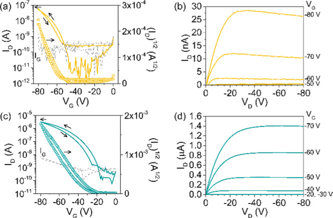
Transfer characteristics of (a) ADI and (c) ADAI for VD = −60 V; dashed lines represent the leakage current. Output characteristics of (b) ADI and (d) ADAI.
The organic thin films deposited on the OFET substrates were also characterized using out-of-plane X-ray diffraction (Figure 4). The powder diffraction pattern showed a good correlation with that obtained from the XRD data of the above-discussed solids. Therefore, the molecular packing in the films is consistent with that previously depicted in Figure 2. Besides, the diffractograms showed only a set of periodic peaks, indicating the existence of a prevalent crystalline phase in the thin films. Accordingly, taking the indexation of the crystalline planes and assuming that the out-of-plane reflections correspond to planes parallel to the substrate, we can get an approximation of how the molecules are oriented on the substrate surface (Figure 4).61 As far as ADI molecules are concerned, they adopt an edge-on orientation, standing on their short edge, with their long edge almost orthogonal to the substrate surface. The calculated d-spacing (17.85 Å; 2θ = 4.95°) fits well with this vertical alignment since it is very close to the length of the molecule (16.56 Å). Differently, although ADAI molecules also arrange in an edge-on disposition, the driving force of the hydrogen-bonded self-assembly affects the orientation of the ribbonlike supramolecular ensemble with respect to the substrate. In agreement with this, the long edge of the molecule is more tilted. This leaned positioning is supported by the calculated d-spacing (5.23 Å; 2θ = 8.49°), which is much shorter than the length of the molecule (16.39 Å).
Figure 4.
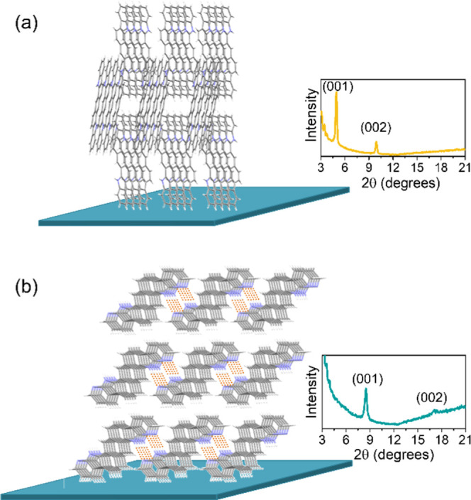
Idealized representation of the molecular arrangement on the OFET substrate surface for (a) ADI and (b) ADAI. The inset shows the XRD diffractograms.
Theoretical Charge Transport Properties of the Crystals
To get a more complete understanding of the charge transport properties of the ADI and ADAI semiconductors, a computational protocol, which combines quantum-chemical calculations (DFT), molecular dynamics (MD) simulations, an analytical Marcus–Levich–Jortner (MLJ) electron-transfer rate expression,62−64 and a master equation approach, was employed to predict hole mobilities assuming an incoherent regime (see the Supporting Information for full details).
Prior to assessing the MLJ electron-transfer rates (kij) and mobilities (μ), it is interesting to discuss the average transfer integrals (⟨tij⟩) and their fluctuations (σtij) due to thermal motions for the different molecular crystal pairs. Note that electronic coupling fluctuations have turned out to be crucial to accurately describe charge and energy transport phenomena in molecular aggregates or crystals.65−67 For the ADI crystal, only four molecular pairs with short intermolecular contacts hold different ⟨tij⟩ values (Figure S4 and Table S1). As expected, ⟨tij⟩ calculated for the parallelly displaced π-stacking dimers (⟨t1,10⟩) with face-to-face π–π interactions is found to present the highest average value (37.7 meV) with a standard deviation (σt1,10) of 14.5 meV. The edge-to-face molecular dimers display ⟨t1,2⟩ ± σt1,2 and ⟨t1,6⟩ ± σt1,6 values of −6.8 ± 16.9 meV and −8.1 ± 10.6 meV, respectively. The relatively large transfer integral fluctuations with respect to the average values are in line with those of other organic semiconducting compounds.68
Compared to ADI, ADAI exhibits more molecular crystal pairs with different and non-negligible ⟨tij⟩ and σtij values (Figure S5 and Table S1). These molecular pairs are mainly governed by edge-to-edge (hydrogen bonding) and face-to-face (π–π) interactions without edge-to-face contacts. It should be stressed that the edge-to-edge interactions commonly result in nonexistent overlap, but in this case, the hydrogen bond-directed self-assembly strengthens these interactions and can open up alternative charge transport pathways. For instance, a relatively important average transfer integral and standard deviation of 3.0 ± 2.6 meV (t1,11 = t1,20) are found for the hydrogen-bonded molecular dimers. Slipped face-to-face dimers that connect parallel columns provide the highest ⟨tij⟩ values (⟨t1,8⟩ = ⟨t1,17⟩ = −12.3 meV) and (⟨t1,12⟩ = ⟨t1,19⟩ = −13.3 meV) with significant fluctuation σtij values (σt1,8 = σt1,17 = 6.5 meV and σt1,12 = σt1,19 = 10.0 meV) close to the average values. For the eclipsed face-to-face π-stacking dimer, a ⟨t1,2⟩ value of 0.0 meV is calculated, whereas an important fluctuation of the transfer integral is obtained (σt1,2 = 57.8 meV). This finding can be easily justified by the periodic oscillation and sensitivity of the transfer integral values with the longitudinal and transversal slippages between molecules (Figure S6).69 Despite the small average transfer integral, a significant charge-transfer rate for this eclipsed face-to-face π-stacking dimer is expected owing to the significant transfer integral fluctuation.
Besides transfer integrals and fluctuations between the different molecular crystal pairs, the calculation of the reorganization energies (internal and external) and the site energy difference (ΔEij) is needed to evaluate the MLJ electron-transfer rate constant and, consequently, the hole mobilities within the crystal structure for ADI and ADAI. Regarding the internal reorganization energy (λint), DFT calculations predict λint values in the same range for both systems, being smaller for ADI (159 meV) than for ADAI (183 meV). External reorganization energies (λext) in organic semiconducting crystals are expected to be lower than λint.70 For both ADI and ADAI, λext is set to be 50 meV according to values reported for other similar systems in the literature.71 Regarding the site energy difference in the crystals, ΔEij deviates from zero due to its dependence on an external electric field (see the Supporting Information). The introduction of an external electric field (F) is necessary to evaluate the mobilities by means of the master equation from the charge drift velocity. The selected F (1 × 10⁵ V cm–1) is set according to values reported in the literature.72
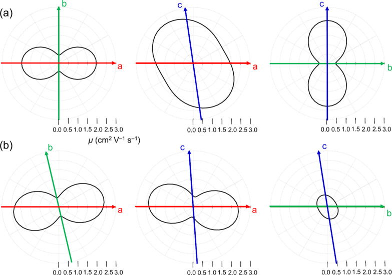
Once all of the parameters involved in the MLJ rate expression are determined, the corresponding rates and, consequently, hole mobilities for the ADI and ADAI semiconductors can be estimated. To do so, a computational protocol based on analytic numerical methods was utilized (see the Supporting Information for further details).72Figure 5 shows the anisotropic hole mobilities calculated for the different crystallographic planes of the ADI and ADAI compounds. The predicted mobilities (∼0.5 to 2.5 cm2 V–1 s–1) are significantly overestimated with respect to the experimental measurements in line with other theoretical studies.71 Note that the calculations are performed using the crystal structures of ADI and ADAI with no defects and, thus, these values can be only used as an upper bound. In the thin films, the morphologies are expected to exhibit different crystalline domains and defects, which are not taken into account in the theoretical estimations. Nonetheless, the theoretical analysis offers insights into the intrinsic charge transport features of the ADI and ADAI crystals. Interestingly, both systems display significant mobilities in the three ab, ac, and bc crystallographic planes. Nevertheless, there are relevant differences: while ADAI exhibits an optimal charge transport direction along the a axis (π-stacked dimers), ADI displays a more isotropic transport in the ab plane in line with the presence of face-to-face and edge-to-face molecular pairs with significant tij values (Figure S4 and Table S1). Despite the difference in the charge transport anisotropy, both ADI and ADAI crystals have μ values in the same range for their optimal directions (∼2.5 cm2 V–1 s–1). The similarity in μ predicted for the ADI and ADAI crystals is seemingly in contrast to the experimental μ values estimated from the OFET devices, where ADAI showed higher mobilities than ADI. This experimental–theoretical discrepancy can be from morphological defects present in the thin films deposited for OFET fabrication. The hydrogen-bonded network present in ADAI produces more robust film morphologies (less disordered) and may explain the higher experimental mobilities observed for ADAI compared to ADI. This is further studied in the annealing experiments discussed below. Additionally, small relative differences in the orientation of neighboring molecules in the thin films compared to the single crystal, especially for π-stacked dimers in ADAI, can cause an enhancement in the charge transport owing to a more efficient orbital overlap (Figure S6).
Figure 5.
Hole mobilities (cm2 V–1 s–1) calculated for the ADI (a) and ADAI (b) crystal structures in the ab (left), ac (middle), and bc (right) crystallographic planes. The parameters used for the calculation were F = 1 × 10⁵ V cm–1 and T = 298 K.
Material and Charge Transport Characterization upon Thermal Treatment
Considering that the stability of the molecular materials is one of the critical issues to be solved in the area of organic electronics, we additionally studied the thermal robustness of the reported materials. The fabricated transistors were annealed at different temperatures following the evolution of their electrical performance and the thin-film morphology. Atomic force microscopy (AFM) images revealed that ADAI thin films showed a granular morphology (Figure 6). This type of microstructure has been previously correlated to good mobilities for similar molecules.57 This contrasts with the morphology observed for the material based on ADI that cannot form hydrogen bonds. Upon heating the substrate, while the ADI thin films experience significant changes in their microstructure, evolving to a granular morphology, the ADAI thin films remain virtually unchanged, with an increase in the grain size being displayed. This evidences the remarkable thermal robustness of the self-assembled material. Interestingly, X-ray diffraction measured on the annealed organic thin films confirmed that the diffractograms were essentially unchanged, although sharper peaks were detected (Figure 6b,c). Therefore, in spite of the morphological transformation observed for ADI, the crystal lattice was the same and it is likely that the crystalline domains grew larger. Although the sharpness of the diffraction peaks also increased in the case of ADAI, the difference is less pronounced.
Figure 6.
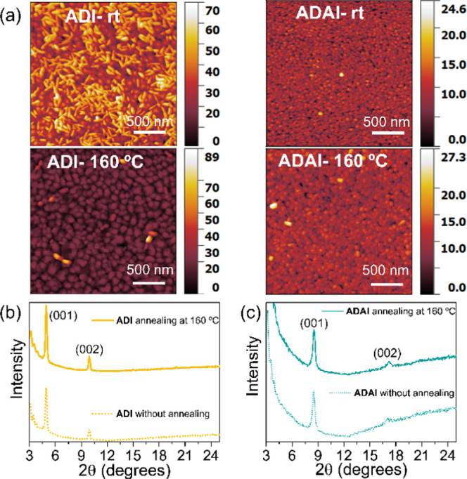
(a) Tapping mode AFM images. (b, c) XRD diffractograms before and after annealing.
The characterization of the transistors during sequential annealing revealed noticeable changes in the ADI transfer characteristics, including a significant reduction of the switch-on voltage and an increase of mobility (Figure 7a). The thermal treatment also confirmed the robustness and high stability of ADAI, whose transfer characteristics displayed a very good reproducibility with a slight decrease in turn-on voltage and an increase in mobility (Figure 7b).
Figure 7.
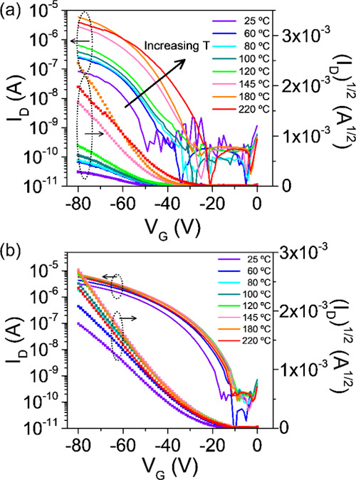
Transfer characteristics at different annealing temperatures for (a) ADI and (b) ADAI.
Table S2 and Figure 8 summarize the OFET parameters for both materials measured at different annealing temperatures. The thermal lability of ADI results in improved mobility that reaches its best value after annealing at 180 °C, presumably due to the previously mentioned increase in the grain size and granular morphology. In contrast, the hydrogen-bonded structure confers stability to ADAI, which also improves its performance but with softer changes, keeping quite consistent higher mobilities throughout most of the annealing process. This would represent a practical advantage for a transistor fabrication process since no thermal treatment would be necessary for the processing of the self-assembled semiconductor. The similar mobilities observed for ADI and ADAI after annealing at more than 150 °C can result from the partial correction of the thin-film defects (especially in the case of the non-hydrogen-bonded ADI) and would be in agreement with the previously discussed similarities in the theoretical mobilities.
Figure 8.
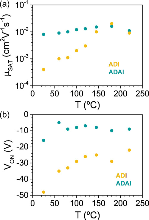
Evolution of (a) the saturated hole mobility (μSAT) and (b) the switch-on voltage (VON) with the annealing temperature.
Finally, it is also interesting to analyze the evolution of the switch-on voltage upon annealing (Figure 8b). Several causes, mainly associated with processes occurring at the hybrid dielectric/organic semiconductor interface (SiO2-OTS/Semiconductor),73 are related to the shift of the switch-on voltage. The dipole orientation and/or dipolar disorder at the interface is correlated to the generation of charge traps. Moreover, charge trapping could also have its origin in the semiconductor itself, either at the interface or in the bulk, and is frequently associated with structural defects or disorder. In this regard, as corroborated by the present comparison, the hydrogen-bonded structure of ADAI can contribute to improving the nanostructural organization, attenuating the disorder in the semiconductor, and improving the transistor performance. Additionally, the semiconductor morphology also has a critical effect on the transistor parameters. For ADI, the thermal treatment causes an improvement in the transistor performance that is clearly associated with the morphological evolution toward a granular structure. This type of morphology is consistently observed for the self-assembled ADAI and results in a better device operation. It is worth noticing that the smaller grains of ADAI (average size 50 nm) enable a more compact packing between grains and better contact with the hybrid dielectric surface enhancing the transistor parameters, which is in line with other previously observed organic semiconductors.74 Conversely, the larger grains formed by ADI (average size 83 nm) and the space between grains seem to reduce the contact between the hybrid dielectric and the semiconductor, requiring a higher voltage to accumulate the charge carriers that lead to the transistor switch-on. Additionally, the lower thin-film roughness of ADAI (roughnessRMS at 160 °C: ADAI = 2.1 nm; ADI = 5.8 nm) is indicative of a less disordered material. In summary, these results reinforce the suitability of hydrogen bond-driven self-assembly for the development of novel organic semiconductors.
Conclusions
We have synthesized two structurally related, pyrrole-based, fused heptacyclic molecules to investigate the effects that hydrogen bond-directed self-assembly has on the structural and electronic parameters governing charge transport. The use of 7-azaindole as a building block for π-conjugated systems has been proved to be a useful synthetic tool for the control of molecular organization through hydrogen bonding. While the non-self-assembled molecule shows a herringbone packing, the self-assembled material displays a slipped columnar packing stabilized by hydrogen bonds. Computational calculations have confirmed that this self-assembled columnar packing efficiently promotes charge transport with mobilities comparable to those for the common herringbone arrangement. Organic field-effect transistors fabricated with the hydrogen-bonded material exhibit better electrical performance in the form of lower switch-on voltages, higher charge carrier mobilities, and a weak dependence of the transfer characteristics on the annealing temperature. In contrast, OFETs made up with the analogous non-self-assembled material require significant thermal treatment to improve their performance. The thermal robustness of the hydrogen-bonded material is also supported by the characterization of the thin-film morphology that presents a granular structure and remains virtually unchanged upon increasing the temperature. In summary, we have demonstrated how molecular organization through hydrogen bonding is an effective strategy for the design of novel organic semiconductors with higher stability and robustness that can contribute to the progress of organic electronics.
Acknowledgments
The authors acknowledge the MCIU of Spain (projects RTI2018-101092-B-I00, PGC2018-099568-B-I00, RED2018-102815-T, and Unidad de Excelencia María de Maeztu CEX2019-000919-M), the Fundación Séneca - Agencia de Ciencia y Tecnología de la Región de Murcia (20959/PI/18), the Generalitat Valenciana (PROMETEO/2020/077 and SEJI/2018/035), and European feder Funds (PGC2018-099568-B-I00) for financial support. M.M.-M. acknowledges Fundación Séneca for a postdoctoral Saavedra Fajardo contract (20406/SF/17). J.C. and J.A. are, respectively, grateful to MCIU for their predoctoral FPI and “Ramón-y-Cajal” Fellowships (RyC-2017-23500).
Supporting Information Available
The Supporting Information is available free of charge at https://pubs.acs.org/doi/10.1021/acsami.0c18928.
Author Contributions
The manuscript was written through the contributions of all authors. All authors have given approval to the final version of the manuscript.
Ministry of Science, Innovation and Universities (MCIU). Fundación Séneca - Agencia de Ciencia y Tecnología de la Región de Murcia. Generalitat Valenciana.
The authors declare no competing financial interest.
Supplementary Material
References
- Hains A. W.; Liang Z.; Woodhouse M. A.; Gregg B. A. Molecular Semiconductors in Organic Photovoltaic Cells. Chem. Rev. 2010, 110, 6689–6735. 10.1021/cr9002984. [DOI] [PubMed] [Google Scholar]
- Ostroverkhova O. Organic Optoelectronic Materials: Mechanisms and Applications. Chem. Rev. 2016, 116, 13279–13412. 10.1021/acs.chemrev.6b00127. [DOI] [PubMed] [Google Scholar]
- Wang C.; Dong H.; Hu W.; Liu Y.; Zhu D. Semiconducting π-Conjugated Systems in Field-Effect Transistors: A Material Odyssey of Organic Electronics. Chem. Rev. 2012, 112, 2208–2267. 10.1021/cr100380z. [DOI] [PubMed] [Google Scholar]
- Xiao L.; Chen Z.; Qu B.; Luo J.; Kong S.; Gong Q.; Kido J. Recent Progresses on Materials for Electrophosphorescent Organic Light-Emitting Devices. Adv. Mater. 2011, 23, 926–952. 10.1002/adma.201003128. [DOI] [PubMed] [Google Scholar]
- Liu Y.-F.; Feng J.; Bi Y.-G.; Yin D.; Sun H.-B. Recent Developments in Flexible Organic Light-Emitting Devices. Adv. Mater. Technol. 2019, 4, 1800371 10.1002/admt.201800371. [DOI] [Google Scholar]
- Lee E. K.; Lee M. Y.; Park C. H.; Lee H. R.; Oh J. H. Toward Environmentally Robust Organic Electronics: Approaches and Applications. Adv. Mater. 2017, 29, 1703638 10.1002/adma.201703638. [DOI] [PubMed] [Google Scholar]
- Baranovskii S. D. Theoretical description of charge transport in disordered organic semiconductors. Phys. Status Solidi (b) 2014, 251, 487–525. 10.1002/pssb.201350339. [DOI] [PubMed] [Google Scholar]
- Novikov S. V.; Vannikov A. V. Hopping Charge Transport in Disordered Organic Materials: Where Is the Disorder?. J. Phys. Chem. C 2009, 113, 2532–2540. 10.1021/jp808578b. [DOI] [Google Scholar]
- Xu X.; Yao Y.; Shan B.; Gu X.; Liu D.; Liu J.; Xu J.; Zhao N.; Hu W.; Miao Q. Electron Mobility Exceeding 10 cm2 V–1 s–1 and Band-Like Charge Transport in Solution-Processed n-Channel Organic Thin-Film Transistors. Adv. Mater. 2016, 28, 5276–5283. 10.1002/adma.201601171. [DOI] [PubMed] [Google Scholar]
- Yavuz I. Dichotomy between the band and hopping transport in organic crystals: insights from experiments. Phys. Chem. Chem. Phys. 2017, 19, 25819–25828. 10.1039/C7CP05297A. [DOI] [PubMed] [Google Scholar]
- Gershenson M. E.; Podzorov V.; Morpurgo A. F. Colloquium: Electronic transport in single-crystal organic transistors. Rev. Mod. Phys. 2006, 78, 973–989. 10.1103/RevModPhys.78.973. [DOI] [Google Scholar]
- Minder N. A.; Ono S.; Chen Z.; Facchetti A.; Morpurgo A. F. Band-Like Electron Transport in Organic Transistors and Implication of the Molecular Structure for Performance Optimization. Adv. Mater. 2012, 24, 503–508. 10.1002/adma.201103960. [DOI] [PubMed] [Google Scholar]
- Podzorov V.; Menard E.; Rogers J. A.; Gershenson M. E. Hall Effect in the Accumulation Layers on the Surface of Organic Semiconductors. Phys. Rev. Lett. 2005, 95, 226601 10.1103/PhysRevLett.95.226601. [DOI] [PubMed] [Google Scholar]
- Tsurumi J.; Matsui H.; Kubo T.; Häusermann R.; Mitsui C.; Okamoto T.; Watanabe S.; Takeya J. Coexistence of ultra-long spin relaxation time and coherent charge transport in organic single-crystal semiconductors. Nat. Phys. 2017, 13, 994–998. 10.1038/nphys4217. [DOI] [Google Scholar]
- Schweicher G.; Olivier Y.; Lemaur V.; Geerts Y. H. What Currently Limits Charge Carrier Mobility in Crystals of Molecular Semiconductors?. Isr. J. Chem. 2014, 54, 595–620. 10.1002/ijch.201400047. [DOI] [Google Scholar]
- Fornari R. P.; Blom P. W. M.; Troisi A. How Many Parameters Actually Affect the Mobility of Conjugated Polymers?. Phys. Rev. Lett. 2017, 118, 086601 10.1103/PhysRevLett.118.086601. [DOI] [PubMed] [Google Scholar]
- Bässler H.; Köhler A.. Charge Transport in Organic Semiconductors. In Unimolecular and Supramolecular Electronics I: Chemistry and Physics Meet at Metal-Molecule Interfaces; Metzger R. M., Ed.; Springer Berlin Heidelberg: Berlin, Heidelberg, 2012; pp 1–65. [DOI] [PubMed] [Google Scholar]
- Coropceanu V.; Cornil J.; da Silva Filho D. A.; Olivier Y.; Silbey R.; Brédas J.-L. Charge Transport in Organic Semiconductors. Chem. Rev. 2007, 107, 926–952. 10.1021/cr050140x. [DOI] [PubMed] [Google Scholar]
- Tessler N.; Preezant Y.; Rappaport N.; Roichman Y. Charge Transport in Disordered Organic Materials and Its Relevance to Thin-Film Devices: A Tutorial Review. Adv. Mater. 2009, 21, 2741–2761. 10.1002/adma.200803541. [DOI] [Google Scholar]
- Sutton C.; Risko C.; Brédas J.-L. Noncovalent Intermolecular Interactions in Organic Electronic Materials: Implications for the Molecular Packing vs Electronic Properties of Acenes. Chem. Mater. 2016, 28, 3–16. 10.1021/acs.chemmater.5b03266. [DOI] [Google Scholar]
- Dong H.; Fu X.; Liu J.; Wang Z.; Hu W. Key Points for High-Mobility Organic Field-Effect Transistors. Adv. Mater. 2013, 25, 6158–6183. 10.1002/adma.201302514. [DOI] [PubMed] [Google Scholar]
- Tsutsui Y.; Schweicher G.; Chattopadhyay B.; Sakurai T.; Arlin J.-B.; Ruzié C.; Aliev A.; Ciesielski A.; Colella S.; Kennedy A. R.; Lemaur V.; Olivier Y.; Hadji R.; Sanguinet L.; Castet F.; Osella S.; Dudenko D.; Beljonne D.; Cornil J.; Samorì P.; Seki S.; Geerts Y. H. Unraveling Unprecedented Charge Carrier Mobility through Structure Property Relationship of Four Isomers of Didodecyl[1]benzothieno[3,2-b][1]benzothiophene. Adv. Mater. 2016, 28, 7106–7114. 10.1002/adma.201601285. [DOI] [PubMed] [Google Scholar]
- Hunter C. A.; Sanders J. K. M. The nature of π-π interactions. J. Am. Chem. Soc. 1990, 112, 5525–5534. 10.1021/ja00170a016. [DOI] [Google Scholar]
- Yao Z.-F.; Wang J.-Y.; Pei J. Control of π–π Stacking via Crystal Engineering in Organic Conjugated Small Molecule Crystals. Cryst. Growth Des. 2018, 18, 7–15. 10.1021/acs.cgd.7b01385. [DOI] [Google Scholar]
- Irimia-Vladu M.; Kanbur Y.; Camaioni F.; Coppola M. E.; Yumusak C.; Irimia C. V.; Vlad A.; Operamolla A.; Farinola G. M.; Suranna G. P.; González-Benitez N.; Molina M. C.; Bautista L. F.; Langhals H.; Stadlober B.; Głowacki E. D.; Sariciftci N. S. Stability of Selected Hydrogen Bonded Semiconductors in Organic Electronic Devices. Chem. Mater. 2019, 31, 6315–6346. 10.1021/acs.chemmater.9b01405. [DOI] [PMC free article] [PubMed] [Google Scholar]
- Głowacki E. D.; Irimia-Vladu M.; Bauer S.; Sariciftci N. S. Hydrogen-bonds in molecular solids - from biological systems to organic electronics. J. Mater. Chem. B 2013, 1, 3742–3753. 10.1039/c3tb20193g. [DOI] [PubMed] [Google Scholar]
- Aakeröy C. B.; Seddon K. R. The hydrogen bond and crystal engineering. Chem. Soc. Rev. 1993, 22, 397–407. 10.1039/CS9932200397. [DOI] [Google Scholar]
- Desiraju G. R. Reflections on the Hydrogen Bond in Crystal Engineering. Cryst. Growth Des. 2011, 11, 896–898. 10.1021/cg200100m. [DOI] [Google Scholar]
- Li Z.-T.; Wu L.-Z.. Hydrogen Bonded Supramolecular Structures; Springer-Verlag, 2015. [Google Scholar]
- Steiner T. The Hydrogen Bond in the Solid State. Angew. Chem., Int. Ed. 2002, 41, 48–76. . [DOI] [PubMed] [Google Scholar]
- Jeffrey G. A.; Saenger W.. Hydrogen Bonding in Biological Structures; SpringerVerlag, 1991; p 581. [Google Scholar]
- Adhikari B.; Lin X.; Yamauchi M.; Ouchi H.; Aratsu K.; Yagai S. Hydrogen-bonded rosettes comprising π-conjugated systems as building blocks for functional one-dimensional assemblies. Chem. Commun. 2017, 53, 9663–9683. 10.1039/C7CC04172A. [DOI] [PubMed] [Google Scholar]
- Aida T.; Meijer E. W.; Stupp S. I. Functional Supramolecular Polymers. Science 2012, 335, 813–817. 10.1126/science.1205962. [DOI] [PMC free article] [PubMed] [Google Scholar]
- Głowacki E. D.; Irimia-Vladu M.; Kaltenbrunner M.; Gsiorowski J.; White M. S.; Monkowius U.; Romanazzi G.; Suranna G. P.; Mastrorilli P.; Sekitani T.; Bauer S.; Someya T.; Torsi L.; Sariciftci N. S. Hydrogen-Bonded Semiconducting Pigments for Air-Stable Field-Effect Transistors. Adv. Mater. 2013, 25, 1563–1569. 10.1002/adma.201204039. [DOI] [PubMed] [Google Scholar]
- Dhar J.; Karothu D. P.; Patil S. Herringbone to cofacial solid state packing via H-bonding in diketopyrrolopyrrole (DPP) based molecular crystals: influence on charge transport. Chem. Commun. 2015, 51, 97–100. 10.1039/C4CC06063F. [DOI] [PubMed] [Google Scholar]
- Irimia-Vladu M.; Głowacki E. D.; Troshin P. A.; Schwabegger G.; Leonat L.; Susarova D. K.; Krystal O.; Ullah M.; Kanbur Y.; Bodea M. A.; Razumov V. F.; Sitter H.; Bauer S.; Sariciftci N. S. Indigo - A Natural Pigment for High Performance Ambipolar Organic Field Effect Transistors and Circuits. Adv. Mater. 2012, 24, 375–380. 10.1002/adma.201102619. [DOI] [PubMed] [Google Scholar]
- Mula S.; Han T.; Heiser T.; Lévêque P.; Leclerc N.; Srivastava A. P.; Ruiz-Carretero A.; Ulrich G. Hydrogen Bonding as a Supramolecular Tool for Robust OFET Devices. Chem. - Eur. J. 2019, 25, 8304–8312. 10.1002/chem.201900689. [DOI] [PubMed] [Google Scholar]
- Gsänger M.; Oh J. H.; Könemann M.; Höffken H. W.; Krause A.-M.; Bao Z.; Würthner F. A Crystal-Engineered Hydrogen-Bonded Octachloroperylene Diimide with a Twisted Core: An n-Channel Organic Semiconductor. Angew. Chem., Int. Ed. 2010, 49, 740–743. 10.1002/anie.200904215. [DOI] [PubMed] [Google Scholar]
- Miao Q.; Lefenfeld M.; Nguyen T. Q.; Siegrist T.; Kloc C.; Nuckolls C. Self-Assembly and Electronics of Dipolar Linear Acenes. Adv. Mater. 2005, 17, 407–412. 10.1002/adma.200401251. [DOI] [Google Scholar]
- Wang M.; Li J.; Zhao G.; Wu Q.; Huang Y.; Hu W.; Gao X.; Li H.; Zhu D. High-Performance Organic Field-Effect Transistors Based on Single and Large-Area Aligned Crystalline Microribbons of 6,13-Dichloropentacene. Adv. Mater. 2013, 25, 2229–2233. 10.1002/adma.201204469. [DOI] [PubMed] [Google Scholar]
- He Z.; Liu D.; Mao R.; Tang Q.; Miao Q. Hydrogen-Bonded Dihydrotetraazapentacenes. Org. Lett. 2012, 14, 1050–1053. 10.1021/ol203404q. [DOI] [PubMed] [Google Scholar]
- Wei Z.; Hong W.; Geng H.; Wang C.; Liu Y.; Li R.; Xu W.; Shuai Z.; Hu W.; Wang Q.; Zhu D. Organic Single Crystal Field-effect Transistors Based on 6H-pyrrolo[3,2–b:4,5–b′]bis[1,4]benzothiazine and its Derivatives. Adv. Mater. 2010, 22, 2458–2462. 10.1002/adma.201000088. [DOI] [PubMed] [Google Scholar]
- Gómez P.; Georgakopoulos S.; Cerón J. P.; da Silva I.; Más-Montoya M.; Pérez J.; Tárraga A.; Curiel D. Hydrogen-bonded azaphenacene: a strategy for the organization of π-conjugated materials. J. Mater. Chem. C 2018, 6, 3968–3975. 10.1039/C8TC00840J. [DOI] [Google Scholar]
- Más-Montoya M.; Gómez P.; Curiel D.; da Silva I.; Wang J.; Janssen R. A. J. A Self-Assembled Small-Molecule-Based Hole-Transporting Material for Inverted Perovskite Solar Cells. Chem. - Eur. J. 2020, 26, 10276–10282. 10.1002/chem.202000005. [DOI] [PubMed] [Google Scholar]
- Ito Y.; Virkar A. A.; Mannsfeld S.; Oh J. H.; Toney M.; Locklin J.; Bao Z. Crystalline Ultrasmooth Self-Assembled Monolayers of Alkylsilanes for Organic Field-Effect Transistors. J. Am. Chem. Soc. 2009, 131, 9396–9404. 10.1021/ja9029957. [DOI] [PubMed] [Google Scholar]
- Frisch M. J.; Trucks G. W.; Schlegel H. B.; Scuseria G. E.; Robb M. A.; Cheeseman J. R.; Scalmani G.; Barone V.; Petersson G. A.; Nakatsuji H.; Li X.; Caricato M.; Ma-renich A. V.; Bloino J.; Janesko B. G.; Gomperts R.; Mennucci B.; Hratchian H. P.; Ortiz J. V.; Iz-maylov A. F.; Sonnenberg J. L.; Williams-Young D.; Ding F.; Lipparini F.; Egidi F.; Goings J.; Peng B.; Petrone A.; Henderson T.; Ranasinghe D.; Zakrzewski V. G.; Gao J.; Rega N.; Zheng G.; Liang W.; Hada M.; Ehara M.; Toyota K.; Fukuda R.; Hasegawa J.; Ishida M.; Nakajima T.; Honda Y.; Kitao O.; Nakai H.; Vreven T.; Throssell K.; Montgomery J. A. Jr.; Peralta J. E.; Ogliaro F.; Bear-park M. J.; Heyd J. J.; Brothers E. N.; Kudin K. N.; Staroverov V. N.; Keith T. A.; Kobayashi R.; Normand J.; Raghavachari K.; Rendell A. P.; Burant J. C.; Iyengar S. S.; Tomasi J.; Cossi M.; Mi-llam J. M.; Klene M.; Adamo C.; Cammi R.; Ochterski J. W.; Martin R. L.; Morokuma K.; Farkas O.; Foresman J. B.; Fox D. J.. Gaussian 16, Revision A.03; Gaussian, Inc.: Wallingford CT, 2016.
- Grimme S.; Antony J.; Ehrlich S.; Krieg H. A consistent and accurate ab initio parametrization of density functional dispersion correction (DFT-D) for the 94 elements H-Pu. J. Chem. Phys. 2010, 132, 154104 10.1063/1.3382344. [DOI] [PubMed] [Google Scholar]
- Grimme S.; Ehrlich S.; Goerigk L. Effect of the damping function in dispersion corrected density functional theory. J. Comput. Chem. 2011, 32, 1456–1465. 10.1002/jcc.21759. [DOI] [PubMed] [Google Scholar]
- Lee C.; Yang W.; Parr R. G. Development of the Colle-Salvetti correlation-energy formula into a functional of the electron density. Phys. Rev. B 1988, 37, 785–789. 10.1103/PhysRevB.37.785. [DOI] [PubMed] [Google Scholar]
- Francl M. M.; Pietro W. J.; Hehre W. J.; Binkley J. S.; Gordon M. S.; DeFrees D. J.; Pople J. A. Self-consistent molecular orbital methods. XXIII. A polarization-type basis set for second-row elements. J. Chem. Phys. 1982, 77, 3654–3665. 10.1063/1.444267. [DOI] [Google Scholar]
- Tomasi J.; Mennucci B.; Cammi R. Quantum Mechanical Continuum Solvation Models. Chem. Rev. 2005, 105, 2999–3094. 10.1021/cr9904009. [DOI] [PubMed] [Google Scholar]
- Baumeier B.; Kirkpatrick J.; Andrienko D. Density-functional based determination of intermolecular charge transfer properties for large-scale morphologies. Phys. Chem. Chem. Phys. 2010, 12, 11103–11113. 10.1039/c002337j. [DOI] [PubMed] [Google Scholar]
- Kuster S.; Geiger T. Coupled π-conjugated chromophores: Squaraine dye dimers as two connected pendulums. Dyes Pigm. 2015, 113, 110–116. 10.1016/j.dyepig.2014.08.001. [DOI] [Google Scholar]
- Dorel R.; Grugel C. P.; Haydl A. M. The Buchwald–Hartwig Amination After 25 Years. Angew. Chem., Int. Ed. 2019, 58, 17118–17129. 10.1002/anie.201904795. [DOI] [PubMed] [Google Scholar]
- Clar E.Polycyclic Hydrocarbons; Springer-Verlag Berlin Heidelberg: 1964; p 1. [Google Scholar]
- Boudreault P.-L. T.; Wakim S.; Blouin N.; Simard M.; Tessier C.; Tao Y.; Leclerc M. Synthesis, Characterization, and Application of Indolo[3,2-b]carbazole Semiconductors. J. Am. Chem. Soc. 2007, 129, 9125–9136. 10.1021/ja071923y. [DOI] [PubMed] [Google Scholar]
- Más-Montoya M.; Georgakopoulos S.; Cerón-Carrasco J. P.; Pérez J.; Tárraga A.; Curiel D. Structure–Property Correlation behind the High Mobility of Carbazolocarbazole. J. Phys. Chem. C 2018, 122, 11736–11746. 10.1021/acs.jpcc.8b03878. [DOI] [Google Scholar]
- Curtis M. D.; Cao J.; Kampf J. W. Solid-State Packing of Conjugated Oligomers: From π-Stacks to the Herringbone Structure. J. Am. Chem. Soc. 2004, 126, 4318–4328. 10.1021/ja0397916. [DOI] [PubMed] [Google Scholar]
- Meyer J.; Hamwi S.; Kröger M.; Kowalsky W.; Riedl T.; Kahn A. Transition Metal Oxides for Organic Electronics: Energetics, Device Physics and Applications. Adv. Mater. 2012, 24, 5408–5427. 10.1002/adma.201201630. [DOI] [PubMed] [Google Scholar]
- Martínez Hardigree J. F.; Katz H. E. Through Thick and Thin: Tuning the Threshold Voltage in Organic Field-Effect Transistors. Acc. Chem. Res. 2014, 47, 1369–1377. 10.1021/ar5000049. [DOI] [PubMed] [Google Scholar]
- Bai X.; Zong K.; Ly J.; Mehta J. S.; Hand M.; Molnar K.; Lee S.; Kahr B.; Mativetsky J. M.; Briseno A.; Lee S. S. Orientation Control of Solution-Processed Organic Semiconductor Crystals To Improve Out-of-Plane Charge Mobility. Chem. Mater. 2017, 29, 7571–7578. 10.1021/acs.chemmater.7b02771. [DOI] [Google Scholar]
- Fornari R. P.; Aragó J.; Troisi A. A very general rate expression for charge hopping in semiconducting polymers. J. Chem. Phys. 2015, 142, 184105 10.1063/1.4920945. [DOI] [PubMed] [Google Scholar]
- Barbara P. F.; Meyer T. J.; Ratner M. A. Contemporary Issues in Electron Transfer Research. J. Phys. Chem. A 1996, 100, 13148–13168. 10.1021/jp9605663. [DOI] [Google Scholar]
- Jortner J. Temperature dependent activation energy for electron transfer between biological molecules. J. Chem. Phys. 1976, 64, 4860–4867. 10.1063/1.432142. [DOI] [Google Scholar]
- Aragó J.; Troisi A. Regimes of Exciton Transport in Molecular Crystals in the Presence of Dynamic Disorder. Adv. Funct. Mater. 2016, 26, 2316–2325. 10.1002/adfm.201503888. [DOI] [Google Scholar]
- Aragó J.; Troisi A. Dynamics of the Excitonic Coupling in Organic Crystals. Phys. Rev. Lett. 2015, 114, 026402 10.1103/PhysRevLett.114.026402. [DOI] [PubMed] [Google Scholar]
- Troisi A.; Orlandi G. Charge-Transport Regime of Crystalline Organic Semiconductors: Diffusion Limited by Thermal Off-Diagonal Electronic Disorder. Phys. Rev. Lett. 2006, 96, 086601 10.1103/PhysRevLett.96.086601. [DOI] [PubMed] [Google Scholar]
- Troisi A.; Orlandi G. Dynamics of the Intermolecular Transfer Integral in Crystalline Organic Semiconductors. J. Phys. Chem. A 2006, 110, 4065–4070. 10.1021/jp055432g. [DOI] [PubMed] [Google Scholar]
- Brédas J. L.; Calbert J. P.; da Silva Filho D. A.; Cornil J. Organic semiconductors: A theoretical characterization of the basic parameters governing charge transport. Proc. Natl. Acad. Sci. U.S.A. 2002, 99, 5804–5809. 10.1073/pnas.092143399. [DOI] [PMC free article] [PubMed] [Google Scholar]
- McMahon D. P.; Troisi A. Evaluation of the External Reorganization Energy of Polyacenes. J. Phys. Chem. Lett. 2010, 1, 941–946. 10.1021/jz1001049. [DOI] [Google Scholar]
- Stehr V.; Fink R. F.; Tafipolski M.; Deibel C.; Engels B. Comparison of different rate constant expressions for the prediction of charge and energy transport in oligoacenes. Wiley Interdiscip. Rev.: Comput. Mol. Sci. 2016, 6, 694–720. 10.1002/wcms.1273. [DOI] [Google Scholar]
- Stehr V.; Pfister J.; Fink R. F.; Engels B.; Deibel C. First-principles calculations of anisotropic charge-carrier mobilities in organic semiconductor crystals. Phys. Rev. B 2011, 83, 155208 10.1103/PhysRevB.83.155208. [DOI] [Google Scholar]
- Dhar B. M.; Özgün R.; Dawidczyk T.; Andreou A.; Katz H. E. Threshold voltage shifting for memory and tuning in printed transistor circuits. Mater. Sci. Eng., R 2011, 72, 49–80. 10.1016/j.mser.2010.11.001. [DOI] [Google Scholar]
- Yang S. Y.; Shin K.; Park C. E. The Effect of Gate-Dielectric Surface Energy on Pentacene Morphology and Organic Field-Effect Transistor Characteristics. Adv. Funct. Mater. 2005, 15, 1806–1814. 10.1002/adfm.200400486. [DOI] [Google Scholar]
Associated Data
This section collects any data citations, data availability statements, or supplementary materials included in this article.


