Abstract
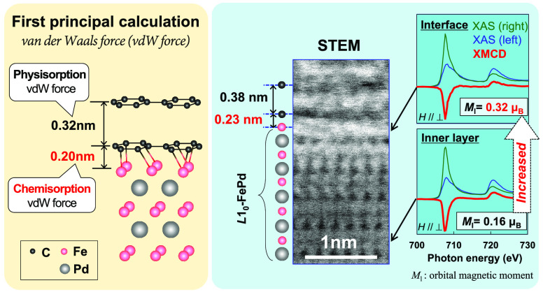
A crystallographically heterogeneous interface was fabricated by growing hexagonal graphene (Gr) using chemical vapor deposition (CVD) on a tetragonal FePd epitaxial film grown by magnetron sputtering. FePd was alternately arranged with Fe and Pd in the vertical direction, and the outermost surface atom was identified primarily as Fe rather than Pd. This means that FePd has a high degree of L10-ordering, and the outermost Fe bonds to the carbon of Gr at the interface. When Gr is grown by CVD, the crystal orientation of hexagonal Gr toward tetragonal L10-FePd selects an energetically stable structure based on the van der Waals (vdW) force. The atomic relationship of Gr/L10-FePd, which is an energetically stable interface, was unveiled theoretically and experimentally. The Gr armchair axis was parallel to FePd [100]L10, where Gr was under a small strain by chemical bonding. Focusing on the interatomic distance between the Gr and FePd layers, the distance was theoretically and experimentally determined to be approximately 0.2 nm. This shorter distance (≈0.2 nm) can be explained by the chemisorption-type vdW force of strong orbital hybridization, rather than the longer distance (≈0.38 nm) of the physisorption-type vdW force. Notably, depth-resolved X-ray magnetic circular dichroism analyses revealed that the orbital magnetic moment (Ml) of Fe in FePd emerged at the Gr/FePd interface (@inner FePd: Ml = 0.16 μB → @Gr/FePd interface: Ml = 0.32 μB). This interfacially enhanced Ml showed obvious anisotropy in the perpendicular direction, which contributed to interfacial perpendicular magnetic anisotropy (IPMA). Moreover, the interfacially enhanced Ml and interfacially enhanced electron density exhibited robustness. It is considered that the shortening of the interatomic distance produces a robust high electron density at the interface, resulting in a chemisorption-type vdW force and orbital hybridization. Eventually, the robust interfacial anisotropic Ml emerged at the crystallographically heterogeneous Gr/L10-FePd interface. From a practical viewpoint, IPMA is useful because it can be incorporated into the large bulk perpendicular magnetic anisotropy (PMA) of L10-FePd. A micromagnetic simulation assuming both PMA and IPMA predicted that perpendicularly magnetized magnetic tunnel junctions (p-MTJs) using Gr/L10-FePd could realize 10-year data retention in a small recording layer with a circular diameter and thickness of 10 and 2 nm, respectively. We unveiled the energetically stable atomic structure in the crystallographically heterogeneous interface, discovered the emergence of the robust IPMA, and predicted that the Gr/L10-FePd p-MTJ is significant for high-density X nm generation magnetic random-access memory (MRAM) applications.
Keywords: L10 structure, FePd, graphene barrier, 2D, chemisorption interface, van der Waals force, interfacial perpendicular magnetic anisotropy
Introduction
The spin injection/diffusion of two-dimensional (2D) systems in the in-plane direction has received considerable attention1 owing to the long spin diffusion length afforded by π-bound conduction in 2D materials such as graphene (Gr).2 The sources of spin injection into 2D systems are primarily metallic materials, resulting in intensive investigations of 2D/metal magnetic material systems for in-plane spin diffusion/conduction/conversion, which include gating,3 the spin–orbit gap,4 the Dzyaloshinskii–Moria interaction,5 and the Rashba effect,6−8 among others.1,9 In contrast, studies on vertical spin conduction in 2D materials, such as magnetic tunnel junctions (MTJs), are scarce. Vertical spin conduction using 2D materials offers several attractive features. For example, according to theory, a large tunnel magnetoresistance (TMR) ratio was predicted for Co (or Ni)/Gr (or h-BN)/Co (or Ni) MTJs,10−13 where 2D materials are tunneling barriers. Interfacial perpendicular magnetic anisotropy (IPMA) was induced in the Co/Gr (or h-BN)/Co interface via orbital hybridization of Cpz, Codxy, and Codx2–dy2.13,14 Furthermore, the resistance–area (RA) product in the vertical direction in the Co/Gr/Co MTJ was reported to be small.15 Large TMR ratios and IPMAs as well as a low RA product in the vertical direction in 2D materials benefit perpendicularly magnetized MTJs (p-MTJs) in nonvolatile magnetic random-access memory (MRAM). In the current industrial production, MRAM employs CoFeB/MgO p-MTJs16 and their multiple layers; that is, [CoFeB/MgO]n p-MTJs.17,18 [CoFeB/MgO]n p-MTJs afford high data retention by IPMA induced by the orbital hybridization of Opz and Fedz2,19 as well as a high TMR ratio20,21 induced by Δ1 coherent tunneling.22,23 The [CoFeB/MgO]n p-MTJs can be used until 1X nm generation MRAM, where 1X nm is the junction diameter of the p-MTJs. However, when setting a goal for ultra-high-density X-nm-generation MRAM, issues regarding the small RA product of the MgO barrier and the high thermal stability of the recording layer must be further considered. If the large bulk perpendicular magnetocrystalline anisotropy (PMA) of L10-ordered alloys24 is combined with the IPMA and low RA product of 2D materials, the present issues can be mitigated. 2D materials (Gr, h-BN, MoS2, WS2, SnS, etc.) have hexagonal crystal symmetries, which are crystallographically heterogeneous against tetragonal L10-ordered alloys. To exploit tetragonal L10-ordered alloys having a large PMA,24 the interface of “hexagonal 2D materials” and “tetragonal L10-ordered alloys” must be uncovered. Crystallographically heterogeneous hexagonal-2D materials and tetragonal-L10-ordered alloys provide an avenue for the further development of scaling in spintronics research in p-MTJs. However, reports of 2D materials combined with L10-ordered alloys are scarce. Large PMAs have been reported in many L10-ordered alloys.24 Among them, L10-FePd25 and L10-MnGa26 have lower magnetic damping constants (αeff). A small αeff reduces the spin-transfer torque27 switching current, which reduces the energy consumption during operation; hence, L10-FePd was used in this study. The aim of this study is to unveil the detailed interfacial atomic structure and IPMA of the crystallographically heterogeneous Gr/FePd interface using interface-specific analyses and describing a physical picture of a complex interface by comparing the experimental data with a first-principles calculation based on the van der Waals (vdW) force. Finally, the data retention characteristics were calculated by assuming an extremely small Gr/FePd recording dot (10 nm in diameter and 2 nm thickness) for high-density MRAM via micromagnetic simulation.
Results and Discussion
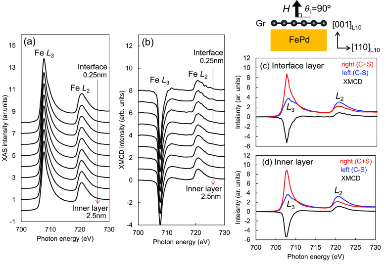
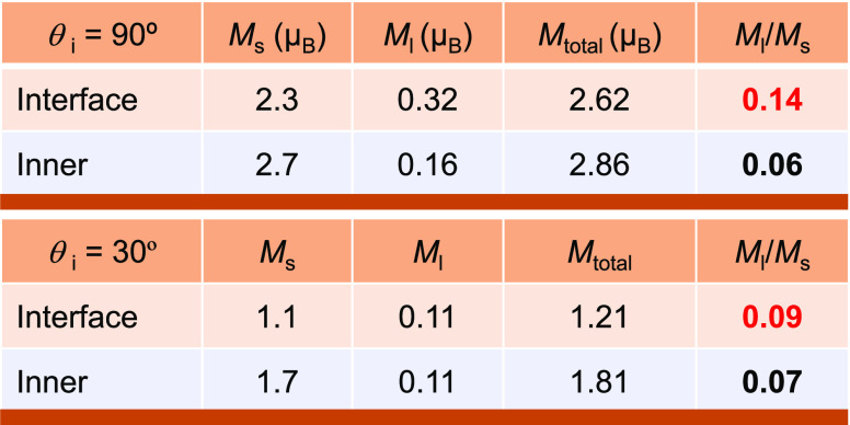
The stacking structure of the sample is Gr/L10-FePd, where Gr is hexagonal and L10-FePd is tetragonal structures. Gr was grown by chemical vapor deposition (CVD), and L10-FePd (31 nm) was grown by radio frequency (r.f.) magnetron sputtering on the SrTiO3(100) substrates.28 The interfacial electric and magnetic properties were evaluated using fluorescence yield depth-resolved soft X-ray absorption spectroscopy (XAS) and soft X-ray magnetic circular dichroism (XMCD) spectroscopy, respectively. The soft X-ray has an advantage for analyzing the interface with a Gr capping layer because a soft X-ray has a shallow penetration depth. Fe L2- and L3-edge XAS and XMCD spectra were measured to characterize the Fe states in the FePd layer. Figure 1 shows the L2,3-edge spectra with different λ ranging from 0.25 to 2.50 nm. A magnetic field (H) was applied at θi = 90°, which is in the perpendicular direction. The details of the measurement setup are explained in the Methods section. The XAS spectra were obtained by averaging the right and left circularly polarized X-rays (Figure 1a). The Gr/FePd bilayer sample was stored under atmospheric pressure and room temperature (RT) for more than one year. No peaks related to Fe oxidation were observed in the XAS, even when measured using high-intensity X-rays of high-energy synchrotron radiation, which is much higher than our previous X-ray photoelectron spectroscopy (XPS) measurements in the lab.28 This result implies that Gr completely prevents the oxidation of FePd. The depth-resolved XMCD spectrum showed that the area ratio of the Fe L2-edge was larger than that of the Fe L3-edge from the inner layer to the surface layer (Figure 1b). The extracted spectra of the right/left circularly polarized XAS spectra and XMCD spectra at the interface and inner layer are shown in Figure 1c and d, respectively. Table 1 lists the spin magnetic moment (Ms), orbital magnetic moment (Ml), their summation (Mtotal = Ms + Ml), and their ratio (Ml /Ms) for the interface and inner layers. The magnetic parameters in Table 1 were deduced from the sum rule29,30 by fitting the XMCD spectra of the interface and inner layers, respectively. The value of Ms of Fe in FePd, which is in contact with the Gr layer, was smaller than that at the inner layer. The decrease of Ms can be considered as a chemical bonding resulting from an orbital hybridization of Fe d-orbitals and C p-orbitals might have decreased Mtotal. In fact, it has been reported31 that a decrease in Ms was experimentally observed at the interface between a hexagonal-Gr and 3-fold symmetry Ni bilayer. On the contrary, Ml of Fe in FePd was twice as large as that at the interface (@inner: Ml = 0.16 μB → @interface: Ml = 0.32 μB), and consequently, Ml /Ms at the interface was more than twice that at the interface (@inner FePd: Ml/Ms = 0.06 → @Gr/FePd interface: Ml/Ms = 0.14). Depth-resolved XMCD spectral analyses for θi = 90° revealed that Ms decreased and Ml of Fe in FePd was enhanced at the FePd/Gr interface.
Figure 1.
Fe L3- and L2-edge spectra with different λ ranging from 0.25 to 2.5 nm for θi = 90°. A magnetic field was applied in the out-of-plane direction (θi = 90°). (a) Depth profiles for an X-ray absorption (XAS) spectrum obtained by averaging right/left circularly polarized X-rays. (b) Depth profile of an X-ray magnetic circular dichroism (XMCD) spectrum obtained based on differences in circularly polarized XAS. XAS and XMCD spectra at the (c) interface and (d) inner layer.
Table 1. Spin Moment (Ms), Orbital Magnetic Moment (Ml), Their Summation (Mtotal = Ms + Ml), and Their Ratio (Ml/Ms) for Interface and Inner Layer Deduced by Fitting of XMCD Spectra Using Sum Rulesa.
At θi = 90°, the Ml/Ms at the interface was more than double that at the inner layer. Ml/Ms at θi = 90° was higher than that at 30°, indicating that there was anisotropy of the Ml in the perpendicular direction. The relatively small Ms at θi = 30° indicates that the external magnetic field was applied to the hard axis.
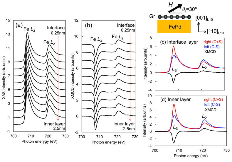
The spin–orbit interaction in Gr was increased owing to the proximity effect upon contact with magnetic materials.32−34 This spin–orbital coupling at the interface is expected to result in uniaxial magnetic anisotropy. Then, to clarify the emergence or not of IPMA, the anisotropic property of Ml was investigated by rotating H. Figure 2 shows the depth-resolved XAS and XMCD for θi = 30°. θi = 30° represents H rotated by 30° from the in-plane direction. The geometry of θi can be confirmed in the Methods section. As shown in Table 1, Ms at the interface was smaller than that in the inner layer, which can be explained as same as that at θi = 90°. It is noteworthy that Ml/Ms at the interface for θi = 90° is obviously larger than that at θi = 30° (@Gr/FePd interface, 90°: Ml/Ms = 0.14 → 30°: Ml/Ms = 0.09). Classically, anisotropic Ml contributes to the uniaxial magnetocrystalline anisotropy energy (MAE). The uniaxial MAE can be described as E(x) – E(z), where E(x) and E(z) are the MAEs to x- and y-axes, respectively. The relation between uniaxial MAE and anisotropic Ml is roughly described using the spin–orbit constant (ξ) as E(x) – E(z) ≅ ξ(Ml(z) – Ml(x))/4 μB, where Ml(x) and Ml(z) are Ml for the x- and z-axes, respectively.35 Thus, depth-resolved XMCD analyses from two directions (θi = 30° and 90°) uncovered that the IPMA emerged by perpendicularly anisotropic Ml at the FePd/Gr interface. A detailed discussion of the contribution ratio of Ml to IPMA by considering exchange splitting at the Fermi level36 will be discussed separately.37
Figure 2.
Depth-resolved (a) X-ray absorption (XAS) and (b) X-ray magnetic circular dichroism (XMCD) and typical spectra at the (c) interface and (d) inner layer. The magnetic field was rotated 30° from the in-plane direction (θi = 30°).
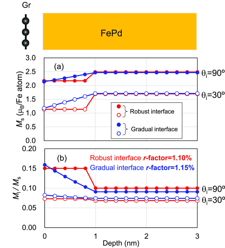
Figure 3 shows the fitting results of the depth dependence of Ms and Ml/Ms in Gr/FePd. To investigate the trends in Ms and Ml/Ms at the Gr/FePd interface, fitting was performed by assuming robust and gradual interfaces for θi = 90° and 30°, respectively. A gradual interface implies that the magnetic properties (Ms and Ml/Ms) at the interface change monotonically, whereas a robust interface implies that the magnetic properties change abruptly. The r-factor was calculated using the following formula:
| 1 |
where “exp” and “sim” are the experimental and simulated values, respectively. The r-factor reflects fitting accuracy, and a smaller r-factor indicates a better fit. The robust and gradual r-factors were 1.10% and 1.15%, respectively. From this fitting, either a robust or gradual interface can be interpreted; however, a robust interface makes the matching rate better.
Figure 3.
Fitting by the sum rule for depth-resolved X-ray magnetic circular dichroism (XMCD) spectra. (a) Ms and (b) Ml/Ms of Gr/FePd. The fitting was performed for the robust and gradual interfaces for θi = 90° and 30°.
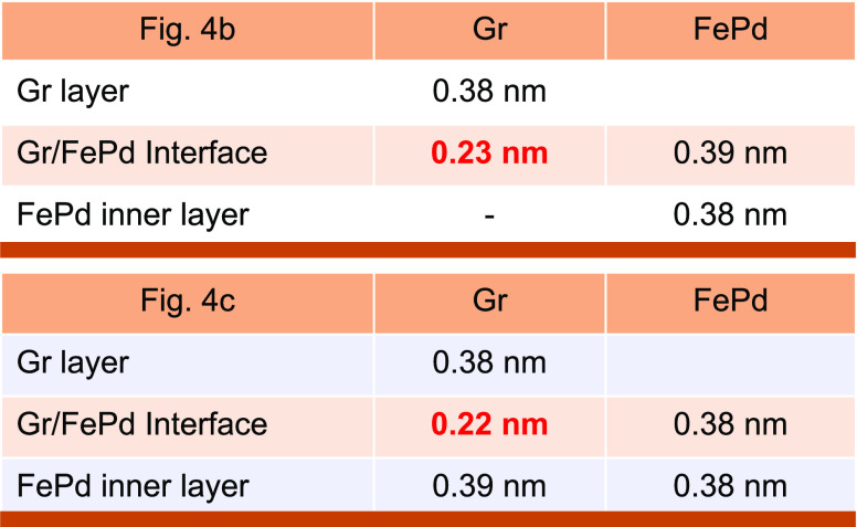
To understand the perpendicularly anisotropic Ml that emerges at the interface, the interfacial structure in atomic resolution was investigated using cross-sectional scanning transmission electron microscopy (STEM) observations. In STEM observations, three different detectors were used to obtain the bright-field (BF), annular bright-field (ABF), and high-angle annular dark-field (HAADF) images; their acceptance angles were 0–10.1, 10.1–79.5, and 79.5–200.0 mrad, respectively (Figure 4a). It is advantageous to use various detectors simultaneously because the Gr/FePd bilayer is composed of “light” and “heavy” elements. Figure 4a shows a schematic illustration of the detector setup with the STEM diffraction patterns. The BF detector can most effectively visualize light elements owing to the low acceptance angle. However, the BF detector also includes unnecessary information such as lattice fringes and Fresnel fringes caused by the interference between the transmitted and diffracted waves. In addition, the contrast in the BF-STEM image was frequently inverted owing to the dynamic diffraction effect and phase-contrast transmission characteristics. Although annular detectors remove unnecessary information, the brightness of the images slightly decreases. The BF detector effectively visualizes light elements, and the annular detector effectively visualizes light and heavy elements; both detectors are necessary for observing the Gr/FePd bilayer. In the case of the annular detector, the ABF-STEM can accurately visualize carbon in Gr and HAADF-STEM can accurately visualize the position of heavy elements of Fe and Pd in FePd. Optimal observation parameters such as focusing/acceleration-voltage/astigmatism exist in each detector; here, the observation conditions are in between. STEM images for the electron incident direction of [110]L10 are shown in Figure 4b and c. In the ABF-STEM images shown in Figure 4b and c, dark dots exist as indicated by the dashed orange arrows. These dots disappeared in the HAADF-STEM images, indicating that the dark dots in the ABF-STEM image represent carbon in Gr. The HAADF-STEM image of heavy elements confirmed the presence of Fe and Pd atoms in the FePd layer, which were arranged alternately in the perpendicular direction (Figure 4b and c). This highly alternating arrangement of Fe and Pd atoms results in a high degree of L10-ordering, which induces the high bulk PMA. The surface layer of FePd was obscure in the HAADF-STEM image, as shown in Figure 4b and c; hence, the contrast was adjusted to visualize the interface on the FePd side (Figure 4d). As a result, it was discovered that the outermost surface atom of FePd was identified primarily as Fe rather than Pd. Fe termination is beneficial because, in an Fe-based L10-ordered alloy, it was observed that the TMR ratio was higher when Fe, instead of a precious metal, was terminated at the interface.38 The interatomic distances of the Gr and FePd layers were evaluated by line profiles in the out-of-plane direction. Figure 4e shows the line profiles from the dashed square area marked in Figure 4b. The distance between the outermost Fe layer in FePd and the first layer of Gr was approximately 0.23 nm. The interatomic distance in the out-of-plane direction of the FePd unit cell was approximately 0.38 nm in the HAADF-STEM images. The out-of-plane distances estimated from the STEM images are listed in Table 2. The bright contrast ⟨A⟩ at FePd in the ABF-STEM image is attributed to the strain from Gr and/or overlapping of heavy and light atoms due to the thickness of the STEM samples (Figure 4f). Figure 4c shows another region of the STEM sample. It was confirmed that this region contained three Gr layers on the FePd layer, and the interatomic distance between the Fe in FePd and carbon of Gr was 0.22 nm, which is consistent with the observation in Figure 4b. The interatomic distance between the second and third Gr layers was approximately 0.38 nm, which was larger than that of the interatomic distance between first Gr layer and Fe layer in FePd.
Figure 4.
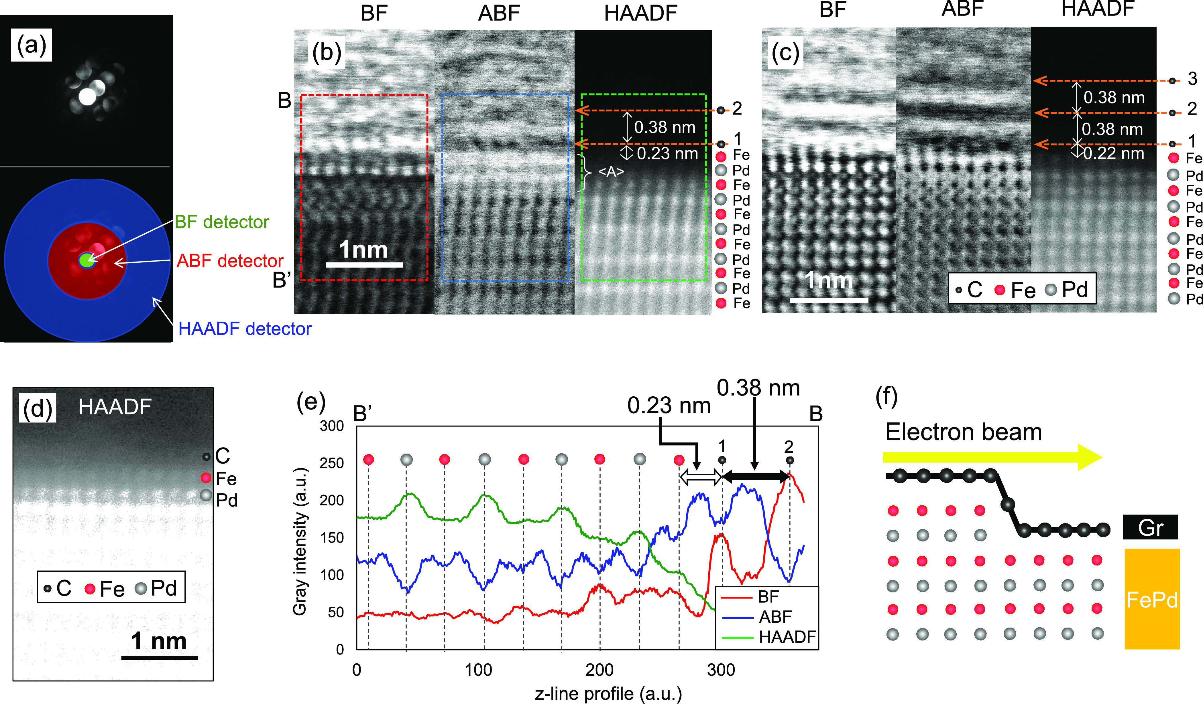
Cross-sectional scanning tunnel electron microscopy (STEM) observations using three different detectors: bright-field (BF), annular bright-field (ABF), and high-angle annular dark-field (HAADF). The incidence of the electron beam is [110]L10. (a) Acceptance angles for BF, ABF, and HAADF were 0–10.1, 10.1–79.5, and 79.5–200 mrad, respectively. STEM observation for (b) single or bilayer graphene and (c) trilayer graphene. (d) Visualization of the interface of the FePd-side HAADF-STEM image by contrast adjustment. The outermost surface atom of FePd was identified primarily as Fe rather than Pd. (e) z-line profiles of the out-of-plane direction obtained from STEM images in (b). z-line profile averaged from the x-direction in the dashed square area. (f) Schematic illustration of electron beam incident direction to the step–terrace interface formed at the Gr/FePd layer.
Table 2. Interatomic Distance to the Out-of-Plane Direction Deduced from Scanning Tunnel Electron Microscopy (STEM) Images of Bilayer and Trilayer Gr in Figure 4b and c, Respectivelya.
The interatomic distance of Gr and FePd layers was approximately 0.2 nm. The shorter interatomic distance compared with graphite (0.355 nm) indicates that the chemisorption-type van der Waals (vdW) force was bonded Gr and FePd. The lattice distance to the perpendicular direction of FePd is almost constant (approximately 0.38 nm).
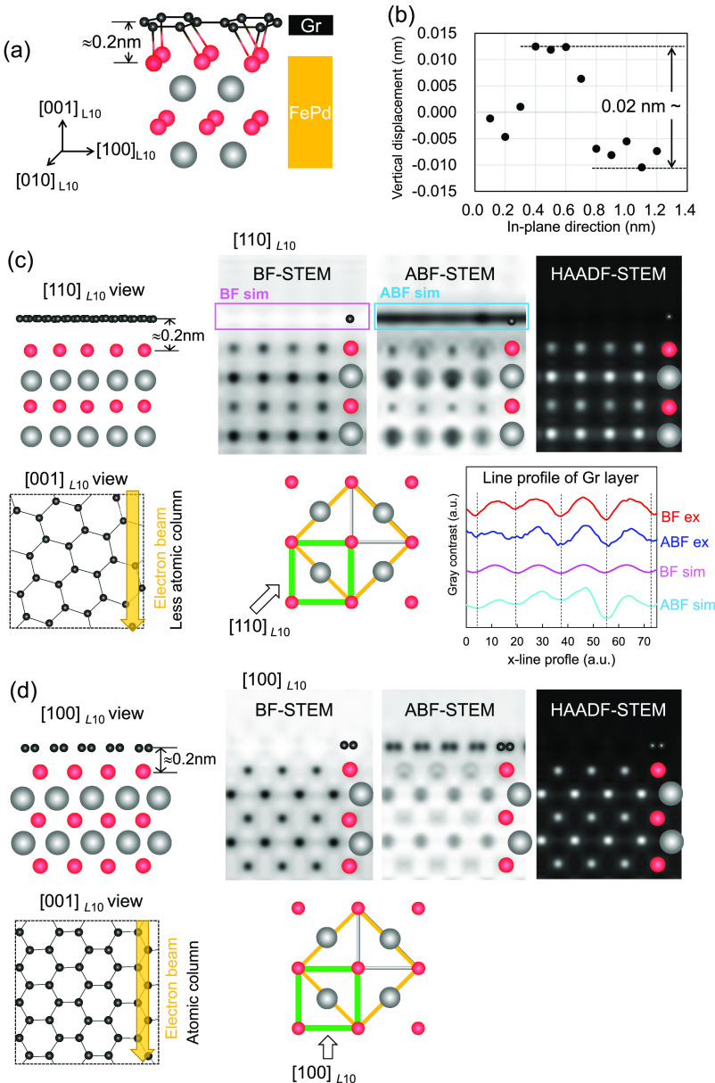
To understand the experimentally observed STEM images, the atomic positions and interatomic distances at the Gr/FePd interface were computationally predicted using first-principles calculations. First-principles structural optimization using the VASP code with PBE39 for exchange–correlation was performed, and Grimme’s DFT-D2 method40 for the vdW interaction was used. The HAADF-STEM image (Figure 4d) reveals that the outermost surface atom of FePd was primarily Fe. Then, the possible supercells of Fe atoms, covered periodically by hexagonal Gr, were investigated. The calculations were performed using three layers of FePd and mono- and bilayer Gr. During the calculation, the atomic positions of the lower end of the three layers of FePd were fixed, and those at upper FePd and Gr layers were relaxed. The energy at each atomic position was calculated by rotating tetragonal L10-FePd toward hexagonal Gr. Consequently, an energetically stable atomic configuration of the crystallographically heterogeneous Gr/L10-FePd interface was proposed. A schematic illustration of the three-dimensional view of the atomic positions is shown in Figure 5a. The atomic relationship between carbon and Fe has been determined theoretically. The Gr armchair axis is parallel to FePd [100]L10, where Gr has a small strain by influence of chemical bonding.37 The interatomic distance in the first layer of Gr and the Fe layer of FePd was determined to be approximately 0.2 nm, which is consistent with the experimentally observed interatomic distances in the BF- and ABF-STEM images (Figure 4b and c). The interatomic distance in the first and second Gr upper layers becomes larger (≈0.32 nm), which roughly agrees with the experimentally confirmed interatomic distance of 0.38 nm (Figure 4b and c). The interatomic distance in the Gr/FePd layer was shorter than that in the upper Gr layers. The interatomic distance in the Gr upper layers (≈0.32 nm) is close to that in graphite (0.355 nm),41 which indicates that the upper Gr layers have physisorption-type vdW forces. In the case of 3-fold symmetric crystal interfaces such as h-BN or Gr/Co,12,13 the interatomic distance was short, and a chemisorption-type vdW force with strong orbital hybridization was observed. Therefore, shortening the interatomic distance at the Gr/FePd interface resulted in a chemisorption-type vdW force with strong orbital hybridization. Figure 5b shows the calculated local vertical displacement of each carbon at the first Gr layer as a function of the in-plane direction. The average displacement of the vertical direction was set to zero (Figure 5b). The maximum displacement in the vertical direction was approximately 0.02 nm. There are many carbons coordinated with respect to Fe atoms in L10-FePd owing to the crystallographically heterogeneous interface, and the strength of the orbital hybridization is dependent on the bonding length. Note that vertical displacement is observed only in the first layer of Gr and almost no influence on the upper second layer of Gr. The influence of FePd on the upper Gr layers is low, and as a result, orbital hybridization weakens. The influence of orbital hybridization from FePd is localized to an extremely short distance, which is evidence of robustness. In the calculation, it was indicated that shortening the interatomic distance induces robust orbital hybridization only at the interface between FePd and first layer of Gr, which is consistent with the experimental XMCD and STEM results.
Figure 5.
Atomic positions calculated via first-principles calculation based on van der Waals (vdW) force. (a) Stable structure of a crystallographically heterogeneous Gr/FePd interface of the 3D image. The armchair axis of Gr is parallel to the FePd [100]L10. (b) Calculated vertical displacement versus in-plane direction for the first layer of Gr taking into consideration the many coordinations of Fe and C atoms at the interface. (c) Simulated BF, ABF, and HAADF-STEM images from electron beam incident [110]L10. The atomic model of the cross-sectional image [110]L10 view of Gr/FePd and in-plane image [001]L10 view for only carbon atoms. In the [001]L10 view, the carbon atoms had less of an atomic column arrangement with respect to the incident electron beam. The line profiles to the in-plane direction of the Gr layer are shown. The line profiles were estimated from BF and ABF-STEM images in the experiment (4b), which is described as BFex (red line) and ABFex (blue line), respectively. The line profiles deduced from simulated BF and ABF-STEM images are described as BFsim (pink line) and ABFsim (light blue line), respectively. The crystal structure of face-centered cubic (fcc) and L10-ordered FePd alloy and relation to the incident direction of the electron beam are indicated. Here, the L10-ordered structure was used and described as [100]L10 and [110]L10. (d) Simulation of STEM images from [100]L10. The two pairs of atomic columns were confirmed from electron beam incident [100]L10.
To determine the atomic position, the experimentally observed STEM images were reproduced by simulation using Win HREM software (HREM Research).42 The atomic coordination deduced from first-principles calculation was used for the STEM image simulation. The STEM simulation was carried out from the electron beam incident on [110]L10 (Figure 5c) and [100]L10 (Figure 5d). The unit cells of L10 and face-centered cubic (fcc) are denoted by the green and orange squares, respectively. From the [110]L10 view (Figure 5c), the first Gr layer in the BF- and ABF-STEM simulated images would be seen as connected contrast among dots. This continuous contrast is roughly consistent with the experimentally observed BF- and ABF-STEM images. The continuity of the Gr layer from the [110]L10 view can be explained by the lower atomic column arrangement against the incident electron beam. The line profile for the in-plane direction was obtained around the first Gr layer in both simulated STEM images and experimentally observed STEM images. The in-plane line profiles from the BF- and ABF-SETM image simulations are denoted BFsim and ABFsim, respectively (Figure 5c). The pink and light blue squares respectively indicate the area of the line profiles for BFsim and ABFsim. The in-plane line profiles deduced from the experimentally observed BF- and ABF-STEM images in Figure 4b are denoted BFex and ABFex, respectively. Line profiles of BFex and ABFex were obtained from the first Gr layer. The gray contrast of the in-plane line profiles corresponds to the sum of the overlapping carbon atoms. For example, when the gray contrast was small, a small number of carbon atoms were aligned in the direction of the electron beam. The line profiles are related to the extent to which the carbon atoms were overlapped; therefore, the line profiles can be used to ensure consistency in structural similarity. The periodicity of gray contrast of in-plane line profiles of carbon in BFex, ABFex, BFsim, and ABFsim was the same. This consistency indicates that the theoretical prediction is in good agreement with the experimentally observed STEM results. Thus, from the interfacial atomic position of Gr grown by CVD on the epitaxial L10-FePd, it is confirmed theoretically and experimentally that the armchair axis of Gr is parallel to that of FePd [100]L10. Hence, it was confirmed that the crystal orientation of hexagonal Gr toward the tetragonal L10-FePd selects an energetically stable structure based on the vdW force. Figure 5d shows STEM simulation images of the electron beam incident from [100]L10. In [100]L10, the carbon forms an atomic column with respect to the electron beam direction, and thus, two pairs of contrasts were simulated in the BF- and ABF-STEM images. The atomic position in the in-plane direction can be determined from a clearer image from the [100]L10 incident.
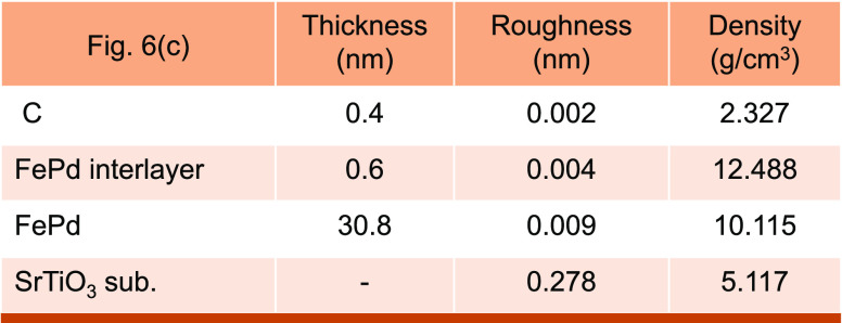
STEM observations reveal the details of the interfacial structure in the local area. The wider areas of the surface and interface were confirmed by atomic force microscopy (AFM), optical microscopy, Raman spectroscopy, and X-ray reflectivity (XRR) analysis. The evaluation of surface morphology by AFM, optical microscopy, and Raman observations was described in the Supporting Information. Here, the content of surface characteristics was briefly explained. AFM was used to evaluate the surface morphology of the L10-FePd film without Gr. The L10-FePd surface was atomically flat, and the average roughness was below 0.4 nm (see the Supporting Information) To evaluate the quality of the Gr layer on the L10-FePd, optical microscopy and Raman spectroscopy observations were carried out (see the Supporting Information). The optical microscopy indicated that the Gr layer showed homogeneous contrast, and a pinhole-like defect was not observed. Raman spectroscopy using the G peak signature showed a homogeneous contrast, indicating that the Gr on L10-FePd was homogeneously covered in a wide area. To evaluate the average number of Gr layers and the density at the Gr/L10-FePd interface, XRR measurements were performed (Figure 6). The XRR can be used to estimate the thickness, roughness, and density of each layer. Not all parameters can be obtained by fitting. Some fixed parameters used for the fitting are required in advance to perform an XRR fitting with accuracy. The thickness of the FePd layer was approximately 31 nm, as measured from cross-sectional HAADF-STEM images. The density of the FePd inner layer was calculated using HAADF-STEM images, which is almost the same as the bulk value. AFM and microscopy observations confirmed that the FePd and Gr layers were flat. These parameters can then be used as fixed values. Thereby, the density at the interface and thickness of the Gr layer were chosen as primary fitting parameters. XRR was measured from 0.5° to 10° in the 2-theta. An angle of more than 6° is caused by graphene, so the fitting was performed by emphasizing the high-angle side. Using the criteria mentioned above, three typical interfacial structures focusing on the interface are presented in Figure 6: (i) the FePd has a continuous density in the vertical direction (Figure 6a); (ii) a gradient high density at the interface (Figure 6b); (iii) a constant robust high density at the interface (Figure 6c). The constant density (Figure 6a) indicates that the fitting curve is under the experimental XRR data. The high-density gradient at the interface (Figure 6b) approached the experimental XRR data. However, beyond 6°, the high-density gradient was slightly mismatched (inset of Figure 6b). As mentioned above, the XRR at a higher angle exceeding 6° was affected by Gr, because Gr is a lightweight element, which causes a density contrast against FePd. Better fitting in whole angle was realized by the constant robust high density at the interface (Figure 6c). The layer information used in the fitting, as shown in Figure 6c, is summarized in Table 3. The thickness of Gr was investigated by changing monolayer to trilayer with fixing the fitting parameters. As a result, the average thickness of the Gr layer was 0.4 nm (Table 3). In other words, Gr was approximately bilayered. This means that the average picture of our sample is described in Figure 4b, which shows the bilayer Gr. In this section, we are going to discuss the meaning of density in XRR. According to the STEM observations (Figures 4b and c), the mass density at the interface of FePd is not high. This was because there was almost no change in the lattice spacing in the out-of-plane and in-plane directions. The density (ρ) can be expressed as
| 2 |
where ρ0, A, λ, NA, Z, and f’ + if’’ are the electron density, atomic weight, wavelength, Avogadro’s number, atomic number, and anomalous scattering factor of the atomic scattering factor, respectively. In eq 2, ρ is proportional to the electron density (ρ0). Therefore, it can be considered that the shortening of the interatomic distance in FePd and the first Gr layers increases ρ0 at the interface. The robustness of ρ0 at the interface (Figure 6c) coincides with that of robust Ml at the interface, which was determined by depth-resolved XMCD analyses (Figure 3b). From these multifaceted analyses, it was revealed that shortening of the interatomic distance produces a robust high ρ0 and chemisorption-type vdW force and that eventually the robust interfacial anisotropic Ml emerges as a consequence of strong orbital hybridization at the Gr/L10-FePd interface.
Figure 6.
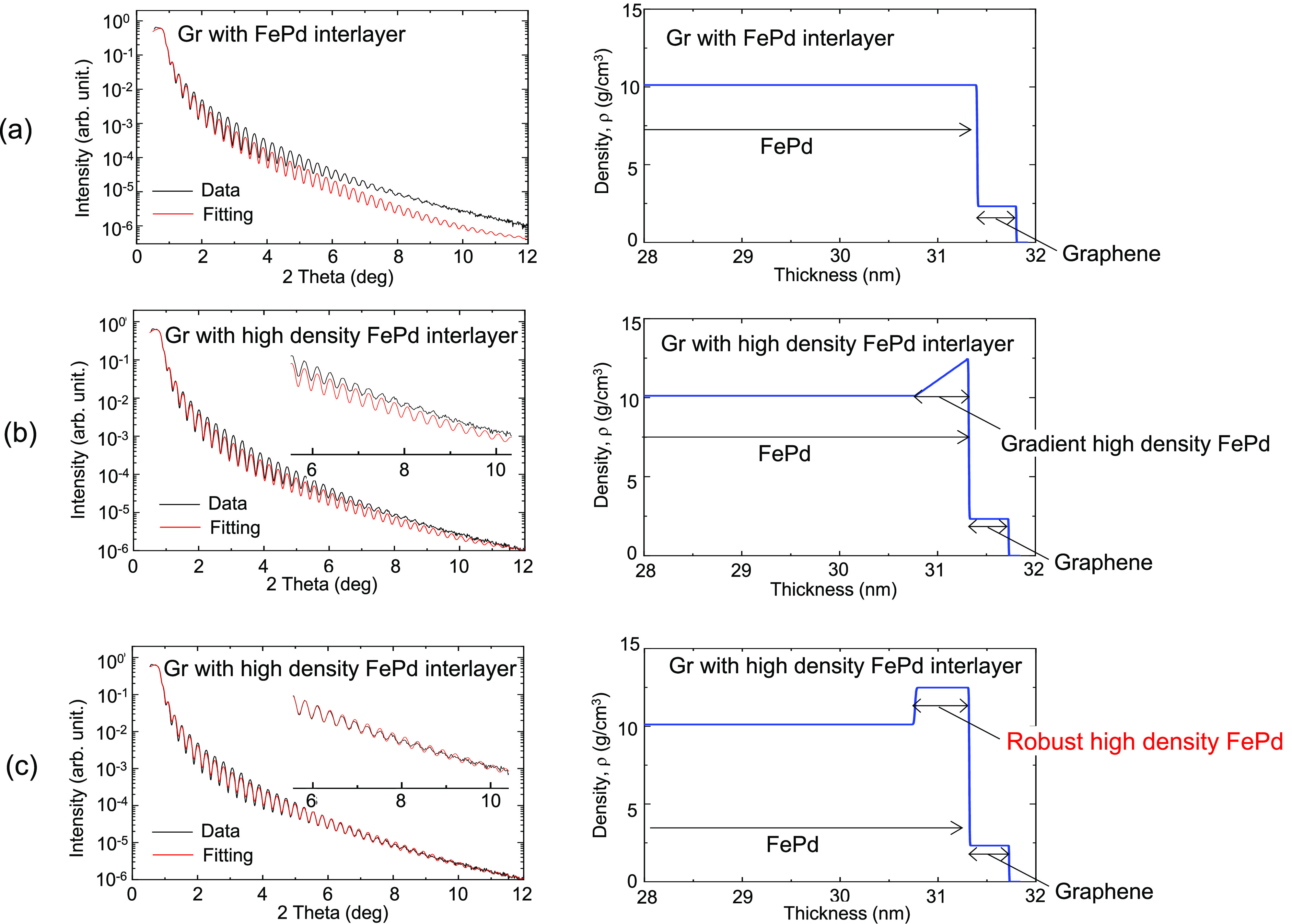
X-ray reflectivity (XRR) measurement of Gr/FePd and three typical fitting results for describing different interfacial structures: (a) continuous mass density, (b) higher mass density gradient, (c) robust high mass density at the FePd side of the interface. The mass density in the vertical axis is proportional to the electron density in XRR fitting equation. At 2 theta above 6 degrees, the XRR data are strongly related to the Gr layer. Fitting in (c) matched well with the experimental data in the whole angle.
Table 3. Thickness, Roughness, and Mass Density (ρ) of Each Layer Deduced by X-ray Reflectivity (XRR) Fitting for the Interfacial Layer with High Robust Mass Density (Figure 6(c))a.
In the XRR measurement, the ρ
of the fitting parameter is proportional to electron density (ρ0).  , where ρ0, A,
λ, NA, Z, and f’ + if’’ are electron density,
atomic weight, wavelength, Avogadro’s number, atomic number,
and anomalous scattering factor of the atomic scattering factor.
Discussion on Gr/L10-FePd Hybrid MTJs for X nm Generation MRAM
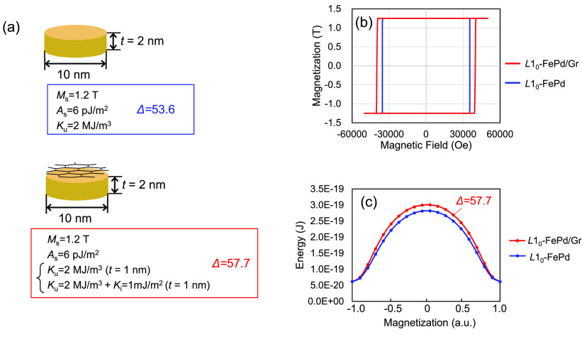
L10-FePd has the advantage of data retention in high-density p-MTJs owing to its high uniaxial MAE. In our previous study,25L10-FePd combined with MgO tunnel barriers required 001 epitaxial growth for Δ1 coherent tunneling. However, the MgO/L10-FePd interface deteriorated due to a large epitaxial lattice mismatch of approximately 10%, which decreased the TMR ratio because of the reduced efficiency of Δ1 coherent tunneling. Consequently, p-MTJs with L10-FePd and a MgO barrier required insertion layers between L10-FePd and MgO to reduce the lattice misfit in a step-by-step manner for the TMR ratio.25 However, the step-by-step technique was limited by large lattice misfit between the L10-FePd and MgO layers. In contrast, our research revealed that, owing to the highly flexible bonding of the vdW force, a flat interface could be formed. Thus, the TMR ratio will not be degraded by the rough interface in the p-MTJs consisting of an L10-FePd recording layer and a Gr tunneling barrier. Focusing on the relationship between scaling and microfabrication damage, the smaller recording layer increases the volume ratio of damage caused by the formation of an oxidation layer during the microfabrication process. The proportion of the damaged layer becomes significant in the X-nm-generation MRAM, where X nm is the diameter of the recording layer. A damaged layer during the microfabrication process is formed on the sidewall at a thickness of approximately 5 nm in the case of CoFeB/MgO p-MTJs.43 The 3d transition metals of Co and Fe have weak oxidation resistance. Conversely, precious metal ordered alloys such as L10-FePd have better oxidation resistance; therefore, precious metals are preferable for reducing sidewall damage. Consequently, it can be considered that the combination of L10-FePd as a recording layer and Gr as a tunneling barrier has an advantage in the X nm generation from the viewpoint of sidewall as well as interfacial damage. As mentioned above, IPMA appears at the FePd/Gr interface. Then, the total PMA is the summation of not only the high bulk PMA of L10-FePd but also the IPMA. To clarify the usefulness of IPMA with the Gr/FePd interface combined with large bulk PMA using L10-FePd, a micromagnetic simulation was performed using a small recording layer. In the Gr/L10-FePd p-MTJ, the FePd recording layer had a circular diameter of 10 nm and a thickness of 2 nm. The size of the recording layer was on the border of the X nm generation. A saturation magnetization of 1.2 T, exchange stiffness constant of 6 pJ/m2, and bulk PMA value of 2 MJ/m3 were used for calculation; these parameters were magnetic properties at RT.44 The IPMA value was set to be 1 mJ/m2.14 The influence of IPMA was set to 1 nm with robustness. The coercive field and thermal stability (Δ) increased by approximately 8% owing to the addition of the IPMA (Figure 7a). The size on the border of the X nm generation demonstrated that the bulk PMA of L10-FePd contributed to the total PMA more than that of the IPMA. It can be considered that the effect of IPMA becomes more apparent when the size is thinner in the X nm generation. The Δ exceeded 57 in the Gr/FePd small dot (Figure 7b), which means that the data retention is more than 10 years. Such high data retention characteristics are difficult to realize by simply using CoFeB/MgO p-MTJs.17,18 In such a small recording layer, not only IPMA of CoFeB/MgO but also the shape magnetic anisotropy (SMA)43 are necessary. In the case of the CoFeB/MgO p-MTJ with IPMA and SMA, optimization of the combination ratio of IPMA and SMA is necessary to reduce the total volume of the magnetic layer for reduction of the switching current. In addition, it is necessary to establish a highly damage-controlled microfabrication process for the CoFeB/MgO hybrid p-MTJs. We believe that there are many breakthrough technologies for realizing the X nm generation, such as the combination of IPMA and SMA in CoFeB/MgO p-MTJs and Gr/L10-FePd hybrid p-MTJs, and each method is a candidate for bridging the technological progress. The micromagnetic simulation of the Gr/L10-FePd p-MTJ proposed that the flexible bond of the vdW force increased the degree of freedom at the interface and is highly valuable for practical use. We think that large bulk PMA combined with IPMA using Gr/L10-FePd p-MTJs is one of the candidate technologies for high-density X-nm-generation MRAM.
Figure 7.
Micromagnetic simulation assuming a small FePd recording layer (thickness = 2 nm; circular diameter = 10 nm) (a) without Gr and with Gr. Calculation was performed using the string method. (b) The magnetization curves by applying magnetic field to perpendicular direction. (c) The thermal stability factor Δ exceeding 57 implies that an information retention period of more than 10 years can be obtained.
Conclusions
Robust anisotropic interfacial Ml emerged at the crystallographically heterogeneous Gr (averagely bilayer)/L10-FePd (31 nm) bilayer. The interatomic distance between the Gr and FePd layers was confirmed theoretically and experimentally as approximately 0.2 nm, which is shorter than the range of the physisorption-type vdW force (0.355 nm in graphite). This shortening of the interatomic distance is due to chemisorption-type vdW force. The short interatomic distance increases the electron density, resulting in strong orbital hybridization, and, eventually, a robust interfacial Ml emerges at the interface. The in-plane crystal orientation of the Gr formed by CVD, which cannot be artificially determined by, for example, the peeling method, was determined theoretically and experimentally as follows: the Gr armchair axis is aligned parallel to the FePd [100]L10, which is an energetically stable interfacial atomic position. Surprisingly, despite the chemisorption-type vdW force, the Gr tolerated its honeycomb structure. The high degree of L10-ordering maintained until the surface of the L10-FePd layer, which faces Gr, is an advantage over L10-FePd/MgO-type MTJs. By micromagnetic simulation, the robust IPMA of the Gr/FePd interface in cooperation with the large PMA of the L10-FePd has the potential to demonstrate data retention over 10 years in ultrasmall p-MTJs, which can be targeted for X-nm-generation MRAM devices. Our concept in this study is extensible to not only graphene but also many hexagonal 2D-based materials, which are advanced technological building blocks that can combine different materials with a high degree of freedom at crystallographically heterogeneous interfaces.
Methods
Gr was formed via CVD, and L10-FePd was grown via r.f. magnetron sputtering (EIKO Co. Ltd.; EW-100NH). The details of the preparation method and concept of the crystallographically heterogeneous interface are described in ref (28). The FePd layer was deposited onto 10 × 10 mm SrTiO3 (001) substrates at RT using a Fe40Pd60 atomic percent (at. %) sintered target (76 mmφ). The composition of the target was adjusted to 40:60 at. % to obtain a 50:50 at. % film composition. The nominal thickness of the FePd film was approximately 30 nm, and the experimentally observed thickness was 31 nm. The FePd films were annealed at 700 °C for 90 min under vacuum using an infrared heater system and cooled to RT. The background pressure prior to the deposition was 2 × 10 –6 Pa. Once exposed to the atmosphere, the samples were transferred to a CVD chamber. The FePd films were heated to 600 °C in a 100 Pa H2 atmosphere at a rate of 300 °C/min and annealed for 15 min to remove the surface oxidation layer. After H2 was removed and the samples were exposed to a 1 Pa C2H2 atmosphere at 600 °C for 15 min, the Gr was formed on the FePd layer.
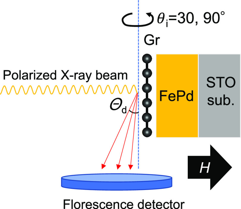
The experimental setup of depth-resolved XAS and XMCD is illustrated in Figure 8. The XAS and XMCD of the Fe L2,3-edges were measured to characterize the Fe states in the FePd layer. The carbon in the Gr layer and Pd in the FePd layer were not measured because of the limitation of the energy region of circularly polarized X-rays at beamline BL-16A. The fluorescence X-rays emitted after XAS were acquired separately at different detection angles (θd) using a 1-megapixel soft X-ray charge-coupled device (BK-501X, BITRAN Corp.). The wavelength (λ) was estimated from the attenuation length (l) and detection angle using the following relation: λ = l sin θd.45 The lowest θd was determined to be ∼0.1°. By analyzing a set of X-ray data recorded at different wavelengths, depth-resolved XAS and XMCD spectra can be obtained. To analyze the magnetic anisotropy, the magnetic field was tilted by θi rotations. θis of 90° and 30° mean that a magnetic field of 0.87 T was applied at 90° and 30° from the in-plane direction, respectively. All experiments were performed in a high-vacuum chamber with a base pressure of 1 × 10⁻⁷ Pa at beamline BL-16A in a photon factory.46 STEM observations were performed using a Thermo Fisher Scientific Titan G2 60-300 Cubed Themis equipped with a Cs corrector for the STEM probe. Epoxy resin was coated on the Gr/FePd/STO and solidified by baking at 100 °C for 30 min in air. After the epoxy resin solidified, a sample for STEM observation was prepared using a focused ion beam (Thermo Fisher Scientific Versa 3D dual beam system). The probe convergence angle, spherical aberration coefficient (Cs), and accelerating voltage were set to 25 mrad, 0 mm, and 300 kV, respectively. The inner and outer angles for the ABF and HAADF detectors were 10.1 and 79.5 mrad and 79.5 and 200 mrad, respectively. These STEM images were computationally reproduced using Win HREM software.41 The atomic positions calculated using first-principles calculations were used for the STEM simulation. The simulated STEM images were compared with the experimentally observed STEM images, and the interfacial atomic positions were determined both experimentally and theoretically. The average Gr thickness and electron density at the interface were investigated by XRR measurements using an X-ray diffractometer (D8 Discover Plus, Bruker AXS GmbH). Line-focused X-rays, which were generated by a 5.4 kW rotating anode generator with a 0.3 mm × 3.0 mm filament, were converged and monochromated using a Göbel multilayer mirror. The mirror reduced the angular spreads to δθ < 2.8 × 10⁻²° for the incidence angle direction of Cu Kα radiation, and the axial divergence was suppressed using Soller slits with angles of 4.0° on both the primary and secondary sides. The incident X-ray beam was formed by the slits and measured 0.05 mm wide and 8.0 mm long. The sample was mounted on an open cradle, and the reflected X-rays were acquired using a multimode detector (EIGER2 R 500 K, DECTRIS AG) after passing through a 0.1-mm-wide antiscattering slit. This multimode detector encompasses an area measuring 77.1 mm × 38.4 mm and controls the active area, similar to the slits. In this experiment, the active area was set to be 0.075 mm wide and 20 mm long. The XRR profile obtained was evaluated via simulation fitting using the DIFFRAC.LEPTOS software package (Bruker AXS GmbH). To demonstrate the practical usefulness of Gr/FePd p-MTJs, the magnetic hysteresis (M – H) loops, energy barrier (E), and thermal stability (Δ) were calculated via micromagnetic simulation,47,48via the string method.49,50 The string method is effective in identifying the minimum energy path between the parallel (P) and antiparallel (AP) states of MTJs. Δ was calculated by taking into consideration the magnetic energy states of the demagnetization energy, Ed, anisotropy energy, Eani, exchange energy, Eexc, and total energy, Eall, for the z-axis (out-of-plane direction). These energy parameters are calculated in 20 points in the free energy landscape between AP, P, and bistable states.
Figure 8.
Experimental setup for fluorescence-yield depth-resolved X-ray absorption (XAS) and X-ray magnetic circular dichroism (XMCD). Fluorescence X-ray emitted after XAS was acquired separately at different detection angles θd with a charge-coupled device. Lowest θd was determined to be ∼0.1°. Magnetic field was tilted by rotations θi and θis of 90° and 30°, respectively, implying that magnetic field of 0.87 T was applied in the out-of-plane direction and rotated 30° from the in-plane direction.
Acknowledgments
This study was partly supported by Center for Spintronics Integrated Systems (CSIS) in Tohoku University, Japan Society for the Promotion of Science (JSPS) Core-to-Core Program (No. JPJSCCA20160005), and cross-appointment project in CSIS Tohoku University. This work has been performed under the approval of the Photon Factory Program Advisory Committee (K.A.) (No. 2019S2-003), nanotechnology platform in Tohoku University (H.N. and M.N.) (No. A-20-TU-0063), and collaborative Research Project of Laboratory for Materials and Structures, Institute of Innovative Research, Tokyo Institute of Technology (S.Y. and H.N.) (No. 76). H.N. thanks Dr. In-T. Bae, University of New York in Binghamton, and Prof Shiraishi, Tokyo Institute of Technology, for fruitful discussions about STEM. H.N. thanks Prof. T. Ono, Kobe University for discussion about theoretical calculation.
Supporting Information Available
The Supporting Information is available free of charge at https://pubs.acs.org/doi/10.1021/acsnano.1c09843.
Surface morphology and quality of Gr/L10-FePd evaluated by AFM (Figure 1S); optical microscopy and Raman spectroscopy observations (Figure 2S) (PDF)
Author Contributions
H.N. conceived this work, designed the interfacial specific analytical experiments, and wrote the first draft. The concept of a crystallographically heterogeneous bilayer structure was proposed by H.N., B.D., and P.S. H.N. grew the L10-FePd, and F.G., M-B.M., B.D., and P.S. fabricated the Gr that was reported previously. The main topic of this work was interfacial analysis, which was assigned as follows. K.A. and H.N. measured and analyzed XMCD and found IPMA. M.N. and H.N. observed cross-sectional STEM, and A.H. simulated the STEM images. H.A., M.U., and H.S. carried out theoretical analysis at interfacial structures by first-principal calculations. S.Y., H.N., and H.M. measured and analyzed XRR. All authors contributed to the discussion of the results and the preparation of the final version of the manuscript.
The authors declare no competing financial interest.
Supplementary Material
References
- Bhimanapati G. R.; Lin Z.; Meunier V.; Jung Y.; Cha J.; Das S.; Xiao D.; Son Y.; Strano S.; Cooper V. R.; Liang L.; Louie S. G.; Ringe E.; Zhou W.; Kim S. S.; Naik R. R.; Sumpter B. G.; Terrones H.; Xia F.; Wang Y.; et al. Recent Advances in Two-Dimensional Materials beyond Graphene. ACS Nano 2015, 9, 11509–11539. 10.1021/acsnano.5b05556. [DOI] [PubMed] [Google Scholar]
- Tombros N.; Jozsa C.; Popinciuc M.; Jonkman H. T.; Wees B. J. v. Electronic spin transport and spin precession in single graphene layers at room temperature. Nature 2007, 448, 571–574. 10.1038/nature06037. [DOI] [PubMed] [Google Scholar]
- Cho S.; Chen Y.-Fu.; Fuhrer M. S. Gate-tunable graphene spin valve. Appl. Phys. Lett. 2007, 91, 123105. 10.1063/1.2784934. [DOI] [Google Scholar]
- Sichau J.; Prada M.; Anlauf T.; Lyon T. J.; Bosnjak B.; Tiemann L.; Blick R. H. Resonance Microwave Measurements of an Intrinsic Spin-Orbit Coupling Gap in Graphene: A Possible Indication of a Topological State. Phys. Rev. Lett. 2019, 122, 04603. 10.1103/PhysRevLett.122.046403. [DOI] [PubMed] [Google Scholar]
- Yang H.; Chen G.; Cotta A. A. C.; N’Diaye A. T.; Nikolaev S. A.; Soares E. A.; Macedo W. A. A.; Liu K.; Schmid A. K.; Fert A.; Chshiev M. Significant Dzyaloshinskii-Moriya interaction at graphene-ferromagnet interfaces due to the Rashba effect. Nat. Mater. 2018, 17, 605–609. 10.1038/s41563-018-0079-4. [DOI] [PubMed] [Google Scholar]
- Gmitra M.; Konschuh S.; Ertler C.; Ambrosch-Draxl C.; Fabian J. Band-structure topologies of graphene: Spin-orbit coupling effects from first principles. Phys. Rev. B 2009, 80, 235431. 10.1103/PhysRevB.80.235431. [DOI] [Google Scholar]
- Li X.; Wu Z.; Liu J. Rashba spin-orbit coupling in graphene monolayer coated by periodic magnetic stripes. Sci. Rep. 2017, 7, 6526. [DOI] [PMC free article] [PubMed] [Google Scholar]
- Gong S. J.; Li Z. Y.; Yang Z. Q.; Gong C.; Duan C.-G.; Chu J. H. Spintronic properties of graphene films grown on Ni(111) substrate. J. Appl. Phys. 2011, 110, 043704. 10.1063/1.3622618. [DOI] [Google Scholar]
- Han W.; Kawakami R. K.; Gmitra M.; Fabian J. Graphene spintronics. Nat. Nanotechnol. 2014, 9, 794–807. 10.1038/nnano.2014.214. [DOI] [PubMed] [Google Scholar]
- Karpan V. M.; Giovannetti G.; Khomyakov P. A.; Talanana M.; Starikov A. A.; Zwierzycki M.; van den Brink J.; Brocks G.; Kelly P. J. Graphite and Graphene as Perfect Spin Filters. Phys. Rev. Lett. 2007, 99, 176602. 10.1103/PhysRevLett.99.176602. [DOI] [PubMed] [Google Scholar]
- Dlubak B.; Martin M.-B.; Weatherup R. S.; Yang H.; Deranlot C.; Blume R.; Shloegl R.; Fert A.; Anane A.; Hofmann S.; Seneor P.; Robertson J. Graphene-Passivated Nickel as an Oxidation-Resistant Electrode for Spintronics. ACS Nano 2012, 6, 10930–10934. 10.1021/nn304424x. [DOI] [PubMed] [Google Scholar]
- Piquemal-Banci M.; Galceran R.; Dubois S. M. -M.; Zatko V.; Galbiati M.; Godel F.; Martin M.-B.; Weatherup R. S.; Petroff F.; Fert A.; Charlier J.-C.; Robertson J.; Hofmann S.; Dlubak B.; Seneor P. Spin filtering by proximity effects at hybridized interfaces in spin-valves with 2D graphene barriers. Nat. Commun. 2020, 11, 5670. 10.1038/s41467-020-19420-6. [DOI] [PMC free article] [PubMed] [Google Scholar]
- Lu H.; Robertson J.; Naganuma H. Comparison of hexagonal boron nitride and MgO tunnel barriers in Fe,Co magnetic tunnel junctions. Appl. Phys. Rev. 2021, 8, 031307. 10.1063/5.0049792. [DOI] [Google Scholar]
- Yang H.; Vu A. D.; Hallal A.; Rougemaille N.; Coraux J.; Chen G.; Schmid A. K.; Chshiev M. Anatomy and Giant Enhancement of the Perpendicular Magnetic Anisotropy of Cobalt-Graphene Heterostructures. Nano Lett. 2016, 16, 145–151. 10.1021/acs.nanolett.5b03392. [DOI] [PubMed] [Google Scholar]
- Li W.; Xue L.; Abruna H. D.; Ralph D. C. Magnetic tunnel junctions with single-layer-graphene tunnel barriers. Phys. Rev. B 2014, 89, 184418. 10.1103/PhysRevB.89.184418. [DOI] [Google Scholar]
- Ikeda S.; Miura K.; Yamamoto H.; Mizunuma K.; Gan H. D.; Endo M.; Kanai S.; Hayakawa J.; Matsukura F.; Ohno H. A perpendicular-anisotropy CoFeB-MgO magnetic tunnel junction. Nat. Mater. 2010, 9, 721–724. 10.1038/nmat2804. [DOI] [PubMed] [Google Scholar]
- Sato H.; Enobio E. C. I.; Yamanouchi M.; Ikeda S.; Fukami S.; Kanai S.; Matsukura F.; Ohno H. Properties of magnetic tunnel junctions with a MgO/CoFeB/Ta/CoFeB/MgO recording structure down to junction diameter of 11 nm. Appl. Phys. Lett. 2014, 105, 062403. 10.1063/1.4892924. [DOI] [Google Scholar]
- Naganuma H.; Miura S.; Honjo H.; Nishioka K.; Watanabe T.; Nasuno T.; Inoue H.; Nguyen T. V. A.; Endo Y.; Noguchi Y.; Yasuhira M.; Ikeda S.; Endoh T. Advanced 18 nm Quad-MTJ technology overcomes dilemma of Retention and Endurance under Scaling beyond 2X nm. VLSI2021 technical digest 2021, T12. [Google Scholar]
- Yang H. X.; Chishiev M.; Dieny B.; Lee J. H.; Manchon A.; Shin K. H. First-principles investigation of the very large perpendicular magnetic anisotropy at Fe|MgO and Co|MgO interfaces. Phys. Rev. B 2011, 84, 054401. 10.1103/PhysRevB.84.054401. [DOI] [Google Scholar]
- Parkin S. S.; Kaiser C.; Panchula A.; Rice P. M.; Hughes B.; Samant M.; Yang S.-H. Giant tunnelling magnetoresistance at room temperature with MgO (100) tunnel barriers. Nat. Mater. 2004, 3, 862–867. 10.1038/nmat1256. [DOI] [PubMed] [Google Scholar]
- Yuasa S.; Nagahama T.; Fukushima A.; Suzuki Y.; Ando K. Giant room-temperature magnetoresistance in single-crystal Fe/MgO/Fe magnetic tunnel junctions. Nat. Mater. 2004, 3, 868–871. 10.1038/nmat1257. [DOI] [PubMed] [Google Scholar]
- Butler W. H.; Zhang X.-G.; Schulthess T. C. Spin-dependent tunneling conductance of Fe|MgO|Fe sandwiches. Phys. Rev. B 2001, 63, 054416. 10.1103/PhysRevB.63.054416. [DOI] [Google Scholar]
- Mathon J.; Umerski A. Theory of tunneling magnetoresistance of an epitaxial Fe/MgO/Fe(001) junction. Phys. Rev. B 2001, 63, 220403R 10.1103/PhysRevB.63.220403. [DOI] [Google Scholar]
- Daalderop G. H. O.; Kelly P. J.; Schuurmans M. F. H. Magnetocrystalline anisotropy and orbital moments in transition-metal compounds. Phys. Rev. B 1991, 44, 12054–12057. 10.1103/PhysRevB.44.12054. [DOI] [PubMed] [Google Scholar]
- Naganuma H.; Kim G.; Kawada Y.; Inami N.; Hatakeyama K.; Iihama S.; Islam K. M. N.; Oogane M.; Mizukami S.; Ando Y. Electrical Detection of Millimeter-Waves by Magnetic Tunnel Junctions Using Perpendicular Magnetized L10-FePd Free Layer. Nano Lett. 2015, 15, 623–628. 10.1021/nl504114v. [DOI] [PubMed] [Google Scholar]
- Mizukami S.; Wu F.; Sakuma A.; Walowski J.; Watanabe D.; Kubota T.; Zhang X.; Naganuma H.; Oogane M.; Ando Y.; Miyazaki T. Long-Lived Ultrafast Spin Precession in Manganese Alloys Films with a Large Perpendicular Magnetic Anisotropy. Phys. Rev. Lett. 2011, 106, 117201. 10.1103/PhysRevLett.106.117201. [DOI] [PubMed] [Google Scholar]
- Slonczewski J. C. Current-driven excitation of magnetic multilayers. J. Mag. Mag. Mater. 1996, 159, L1–L7. 10.1016/0304-8853(96)00062-5. [DOI] [Google Scholar]
- Naganuma H.; Zatko V.; Galbiati M.; Godel F.; Sander A.; Carretero C.; Bezencenet O.; Reyren N.; Martin M.-B.; Dlubak B.; Seneor P. A perpendicular graphene/ferromagnet electrode for spintronics. Appl. Phys. Lett. 2020, 116, 173101. 10.1063/1.5143567. [DOI] [Google Scholar]
- Thole B. T.; Carra P.; Sette F.; van der Laan G. X-ray circular dichroism as a probe of orbital magnetization. Phys. Rev. Lett. 1992, 68, 1943–1946. 10.1103/PhysRevLett.68.1943. [DOI] [PubMed] [Google Scholar]
- Carra P.; Thole B. T.; Altarelli M.; Wang X. X-ray circular dichroism and local magnetic fields. Phys. Rev. Lett. 1993, 70, 694–697. 10.1103/PhysRevLett.70.694. [DOI] [PubMed] [Google Scholar]
- Matsumoto Y.; Entani S.; Koide A.; Ohtomo M.; Avramov P. V.; Naramoto H.; Amemiya K.; Fujikawa T.; Sakai S. Spin orientation transition across the single-layer graphene/nickel thin film interface. J. Mater. Chem. C 2013, 1, 5533–5537. 10.1039/c3tc30872c. [DOI] [Google Scholar]
- Dedkov Yu. S.; Sicot M.; Fonin M. X-ray absorption and magnetic circular dichroism of graphene/Ni(111). J. Appl. Phys. 2010, 107, 09E121. 10.1063/1.3360340. [DOI] [Google Scholar]
- Weser M.; Voloshina E. N.; Horn K.; Dedkov Yu. S. Electronic structure and magnetic properties of the graphene/Fe/Ni(111) intercalation-like system. Phys. Chem. Chem. Phys. 2011, 13, 7534–7539. 10.1039/c1cp00014d. [DOI] [PubMed] [Google Scholar]
- Li W.; Zeng Y.; Zhao Z.; Zhang B.; Xu J.; Huang X.; Hou Y. 2D Magnetic Heterostructures and Their Interface Modulated Magnetism. ACS Appl. Mater. Interfaces 2021, 13, 50591–50601. 10.1021/acsami.1c11132. [DOI] [PubMed] [Google Scholar]
- Bruno P. Tight-binding approach to the orbital magnetic moment and magnetocrystalline anisotropy of transition-metal monolayers. Phys. Rev. B 1989, 39, 865–868. 10.1103/PhysRevB.39.865. [DOI] [PubMed] [Google Scholar]
- Tsujikawa M.; Hosokawa A.; Oda T. Magnetic anisotropy of Fe/Pt(001) and Pt/Fe/Pt(001) using a first-principles approach. Phys. Rev. B 2008, 77, 054413. 10.1103/PhysRevB.77.054413. [DOI] [Google Scholar]
- Uemoto M.; Adachi H.; Ono T.; Naganuma H.. Density functional study of atomic and electronic structures of graphene on FePd (001) surface. To be submitted.to be submitted [Google Scholar]
- Taniguchi Y.; Miura Y.; Abe K.; Shirai M. Theoretical Studies on Spin-Dependent Conductance in FePt/MgO/FePt(001) Magnetic Tunnel Junctions. IEEE Trans. Mag. 2008, 44, 2585–2588. 10.1109/TMAG.2008.2002515. [DOI] [Google Scholar]
- Perdew J. P.; Burke K.; Ernzerhof M. Generalized Gradient Approximation Made Simple. Phys. Rev. Lett. 1996, 77, 3865–3868. 10.1103/PhysRevLett.77.3865. [DOI] [PubMed] [Google Scholar]
- Grimme S. Semiempirical GGA-type density functional constructed with a long-range dispersion correction. J. Comput. Chem. 2006, 27, 1787–1799. 10.1002/jcc.20495. [DOI] [PubMed] [Google Scholar]
- Ishizuka K. A practical approach for STEM image simulation based on the FFT multislice method. Ultramicroscopy 2002, 90, 71–83. 10.1016/S0304-3991(01)00145-0. [DOI] [PubMed] [Google Scholar]
- Delhaes P.Graphite and Precursors. CRC Press. Taylor & Francis Group, A Science Publishers Book, 2001, ISBN; 978–90–5699–228–6. [Google Scholar]
- Watanabe K.; Jinnai B.; Fukami S.; Sato H.; Ohno H. Shape anisotropy revisited in single-digit nanometer magnetic tunnel junctions. Nat. Com. 2018, 9, 663. 10.1038/s41467-018-03003-7. [DOI] [PMC free article] [PubMed] [Google Scholar]
- Mulazzi M.; Chainani A.; Takata Y.; Tanaka Y.; Nishino Y.; Tamasaku K.; Ishikawa T.; Takeuchi T.; Ishida Y.; Senba Y.; Ohashi H.; Shin S.. Temperature dependence of the exchange stiffness in FePd(001) thin films: Deviation from the empirical law. Phys. Rev. B 2008, 77, 224425. 10.1103/PhysRevB.77.224425 [DOI] [Google Scholar]
- Sakamaki M.; Amemiya K. Nanometer-resolution depth-resolved measurement of florescence-yield soft x-ray absorption spectroscopy for FeCo thin film. Rev. Sci. Instrum. 2017, 88, 083901. 10.1063/1.4986146. [DOI] [PubMed] [Google Scholar]
- Amemiya K.; Toyoshima A.; Kikuchi T.; Kosuge T.; Nigorikawa K.; Sumii R.; Ito K. Commissioning of a Soft X-ray Beamline PF-BL-16A with a Variable-Included-Angle Varied-Line-Spacing Grating Monochromator. AIP Conf. Proc. 2009, 1234, 295–298. 10.1063/1.3463193. [DOI] [Google Scholar]
- See http://fujitsu.com/global/about/resources/news/press-releases/2015/0324-01.html for Fujitsu Ltd.
- Naganuma H.; Sato H.; Ikeda S.; Endoh T. Micromagnetic simulation of the temperature dependence of the switching energy barrier using string method assuming sidewall damages in perpendicular magnetized magnetic tunnel junctions. AIP Adv. 2020, 10, 075106. 10.1063/5.0007499. [DOI] [Google Scholar]
- Weinan E.; Weiqing R.; Eijnden E. V. String method for the study of rare events. Phys. Rev. B 2002, 66, 052301. 10.1103/PhysRevB.66.052301. [DOI] [Google Scholar]
- Ren W. E. W.; V.-Eijnden E. Energy barriers to magnetization reversal in perpendicularly magnetized thin film nanomagnets. J. Appl. Phys. 2003, 93, 2275. [Google Scholar]
Associated Data
This section collects any data citations, data availability statements, or supplementary materials included in this article.


