Abstract
Two-dimensional (2D) materials have got extensive attention for multifunctional device applications in advanced nanoelectronics and optoelectronics, such as field-effect transistors, photodiodes, and solar cells. In our work, we fabricated MoTe2–MoS2 van der Waals heterostructure photodetectors with great performance using the mechanical exfoliation method and restack technique. It is demonstrated that our MoTe2–MoS2 heterostructure photodetector device can operate without bias voltage, possessing a low dark current (10 pA) and high photocurrent on/off ratio (>104). Importantly, the room temperature photoresponsivity of the MoTe2–MoS2 photodetector can reach 110.6 and 9.2 mA W–1 under λ = 532 and 1064 nm incident laser powers, respectively. Our results indicate that the van der Waals heterostructure based on 2D semiconducting materials is expected to play an important role in nanoscale optoelectronic applications.
Introduction
Photodetectors are the essential part of optoelectronic systems, playing an important role in various fields in real life, such as photoelectric imaging, optical communications, biomedicine, environmental monitoring, security inspection, military, and so on.1−7 Traditional semiconducting materials, such as Si, Ge, and HgCdTe, have dominant applications in photodetection. However, photodetectors based on these semiconducting materials have disadvantages such as large dark current and complexity, which limits their further optoelectronic applications.8,9
Due to the atomic layer thickness, excellent optical and electrical characteristics of 2D materials, photodetectors of 2D materials, and van der Waals heterostructures have aroused research attention recently.10−12 In comparison with conventional semiconductor materials, 2D materials possess many excellent properties.13 The 2D material layers are connected by van der Waals interactions. Any 2D material can flexibly form a heterostructure with other 2D materials without the consideration of lattice mismatch. This kind of heterojunction has the characteristics of atomic-level thickness, no dangling bonds, and a high-quality interface. The photogeneration and transportation characteristics of carriers are controllable, and the advantages of different 2D materials can be combined.11 The built-in electric field of the 2D p–n junction can effectively suppress the diffusion current; thereby, it can reduce the dark current to a certain extent. Besides, the built-in electric field in the type-II band structure can effectively facilitate the separation of photogenerated electron–hole pairs at the interface, extending the lifetime of the carriers, which is beneficial to the promotion of optical gain and photoresponsivity.14 As the existence of interlayer transitions in type-II band structure, the wavelength of photodetection can be broadened.15 In short, the advantages of the van der Waals heterojunction have led to the rapid development of photodetectors in recent years, and its optoelectronic properties need to be further studied.
In this work, we fabricated MoTe2–MoS2 heterostructure devices based on the type II band structure, where MoTe2 displays p-type characteristics and MoS2 displays n-type characteristics. These two materials have stable and excellent electrical and optoelectrical properties.16−18 The heterojunction formed by MoTe2–MoS2 has rectification characteristics, indicating good formation of the p–n junction. With the existence of the interlayer built-in electric field between these two materials, the dark current maintains in a low level (10 pA). The photocurrent switch-on/off ratio is high (>104) when Vg = 0 V and Vds = 0 V, so it can realize photovoltaic self-driving photodetection. Besides, the room temperature photoresponsivity can reach 110.6 and 9.2 mA W–1 under λ = 532 and 1064 nm incident laser powers, respectively. These performances have reached the advanced level of 2D semiconductor heterostructure devices. Considering the advantages of 2D materials in atomically thickness and flexibility, the photodetectors based on the vertical 2D semiconductor heterostructures have great potential in particular applications, such as wearable optoelectronic devices and integrated photonics.1,13
Results and Discussion
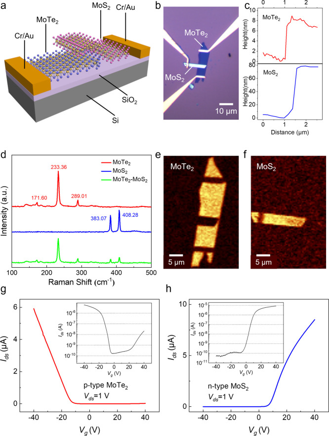
The schematic structure of the MoTe2–MoS2 device is depicted in Figure 1a, and the optical image is depicted in Figure 1b. The height profile of the heterostructure device is depicted in Figure 1c. According to the atomic force microscopy (AFM) measurements, the corresponding thickness of MoTe2 and MoS2 is identified to be 6.7 and 74.4 nm, respectively. Please also see the AFM morphology in Figure S1 in the Supporting Information. We use a Raman spectrometer to characterize the prepared MoTe2–MoS2 heterostructure device. The Raman single-point spectrum is demonstrated in Figure 1d, with the laser wavelength λ = 532 nm and the laser power P = 350 μW. There are three characteristic peaks of MoTe2 measured: the A1g peak (out-of-plane mode) at 171.60 cm–1, the E2g1 peak (in-plane vibration mode) at 233.36 cm–1, and the B2g peak (bulk in-active phonon mode) at 289.01 cm–1. Since B2g does not exist in the monolayer and bulk, MoTe2 is obtained as a few-layer flake.19 There are two characteristic peaks of MoS2: the E2g1 peak at 383.07 cm–1 and the A1g peak at 408.28 cm–1. The Raman shift difference between the two peaks is about 25.21 cm–1, indicating the bulk nature of as-exfoliated MoS2.20 Both MoTe2 and MoS2 can be measured in the overlapped heterostructure area with all characteristic peaks, and the corresponding Raman scanning area mapping is shown in the Figure 1e,f, where the integral center position corresponding to MoTe2 is 233 cm–1, and the integral width is 5 cm–1, the integral center position corresponding to MoS2 is 408 cm–1, and the integral width is 5 cm–1. Figure 1 indicates the good morphology of the van der Waals heterostructure.
Figure 1.
Characterizations of the MoTe2–MoS2 heterostructure device. (a) Schematic structure of the device. (b) Optical microscopy image of the device. (c) Height profile of MoTe2 and MoS2. (d) Raman spectrum of the heterostructure device. (e,f) Raman mapping of integrated intensity of MoTe2 (233 cm–1) and MoS2 (408 cm–1), respectively. (g,h) Transfer curves of the 16.7 nm-thick MoTe2 and 17.3 nm-thick MoS2 field-effect transistor, respectively.
In order to show the carrier polarity of exfoliated MoTe2 and MoS2, we demonstrate transfer curves of the 16.7 nm-thick MoTe2 and 17.3 nm-thick MoS2 field-effect transistors (FETs, Figure S2) in Figure 1g,h, respectively. It is clear that the drain–source current Ids of the MoTe2 device increases with increasing value of negative gate voltage Vg, while the Ids of the MoS2 FET increases with the positive Vg. The result indicates that MoTe2 displays p-type properties and MoS2 displays n-type characteristics. Therefore, a vertical p–n junction is expected to form in the MoTe2–MoS2 heterostructure.
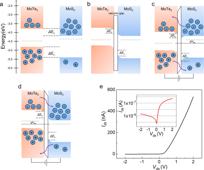
The energy band diagrams of MoTe2 and MoS2 before and after contact are presented in Figure 2a,b, respectively. For MoTe2, the top of the valence band and the bottom of the conduction band are about −4.8 and −3.8 eV, respectively. For MoS2, the top of the valence band and the bottom of the conduction band are about −5.4 and −4.2 eV, respectively.21 The offset of the valence band and conduction band is calculated to be ΔEv = 0.6 eV and ΔEc = 0.4 eV, respectively. Therefore, a type II energy band heterostructure is developed, as depicted in the band diagrams. After the contact between MoTe2 and MoS2, an equilibrium is achieved, which represents that the diffusion and drift currents are in equality but in reversed directions. In order to improve the device quality, we annealed the exfoliated flakes under the protection of an Ar atmosphere (200 °C, 4 h) to remove the polymer residue as much as possible before assembling the heterostructures. The on-state current of the annealed device is significantly increased from 4.5 to 530 nA. The I–V curve of nonannealed device is presented in Figure S3. The I–V characteristic of the MoTe2–MoS2 device under dark conditions is presented in Figure 2e. The Ids and Vds represent the drain–source current and voltage, respectively. It indicates rectification characteristics in Figure 2e at gate voltage Vg = 0. The formula of rectification factor (RF) can be expressed as RF = |Iforward/Ireverse|, and RF is obtained to be 2.5×10² at |Vds| = 2 V. When Vds = 0 V, the Ids is obtained to be −6.7 × 10⁻¹¹ A, which is in a low level. To explain these results, the schematic diagram of the carriers is shown in Figure 2c,d. Under the forward bias voltage, the potential barrier reduces, and the built-in electrical field gets weakened, as the bias voltage is in reverse of the built-in electrical field. Therefore, the p–n junction is disabled to keep in the equilibrium state. Due to the existence of concentration difference, the majority carriers in MoTe2/MoS2 diffuse to the other side and overcome the potential barrier easily. Ultimately large diffusion current is attained. Conversely, under the reverse bias voltage, the potential barrier increases, and the built-in electrical field gets enhanced, as the bias voltage is in the same direction of the built-in electrical field, which promotes transportation of minority carriers to the other side and generation of drift current. The drift current in reverse bias is lower than the diffusion current in forward bias, as the concentration of minority carriers is lower than majority carriers. Therefore, the MoTe2–MoS2 heterostructure device exhibits rectification characteristics of the p–n junction.22
Figure 2.
Energy band diagrams and electrical figures of the MoTe2–MoS2 device. (a) Band diagrams before contact. (b) Band diagrams after contact. (c) Carrier transport band diagrams under forward bias. (d) Carrier transport band diagrams under reverse bias. (e) I–V curves of the MoTe2–MoS2 device; the inset picture represents the I–V characteristics in the logarithmic coordinate. The characterization of this device can be found in Figure S2 in the Supporting Infromation.
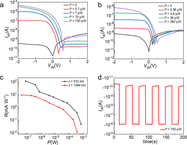
We performed photodetection experiments at different drain-source voltages and incident laser powers to investigate photodetection of the MoTe2–MoS2 device, with the laser wavelengths λ = 532 nm and λ = 1064 nm. The results are shown in Figure 3. Under the illumination of the laser, the carriers are generated and separated at the p–n interface region. Photoresponsivity can be calculated as R = Iph/P, where Iph is photocurrent and P is incident laser power on the MoTe2–MoS2 device. The relationship between the photocurrent and laser power can be expressed as Iph = Pα. By exponential fitting, α is calculated to be 0.394 and 0.338 under the laser wavelengths λ = 532 nm and λ = 1064 nm, respectively. The parameter α indicates the influence of defects or traps in electron–hole pair generation and recombination.21,23 The photoresponsivity of the photodetector can be expressed as R = Iph/P = Pα–1. Photoresponsivity reduces with the increasing incident laser power. The MoTe2–MoS2 heterostructure absorbs photons and generates photocurrent. In addition to the photogeneration, there are recombination processes, photogating effect as the existence of defects or traps, reducing the amount of photogenerated electron–hole pairs obviously with the increase in laser power. The responsivity of the MoTe2–MoS2 device is obtained to be 110.6 mA·W–1 when λ = 532 nm, P = 0.07 μW, and 9.2 mA·W–1 when λ = 1064 nm and P = 0.036 μW. From the formula λ = hc/Eg, where λ is the cutoff wavelength, h is the Planck constant, c is the speed of light in vacuum, Eg is the band gap, we can calculate the cutoff wavelength λ = 1.24 μm and λ = 1.03 μm, corresponding to MoTe2 and MoS2, respectively. Therefore, when the laser of λ = 532 nm irradiates the MoTe2–MoS2 heterostructure device, both MoTe2 and MoS2 can absorb photons, but when the laser of λ = 1064 nm irradiates the MoTe2–MoS2 heterostructure device, only MoTe2 can absorb photons. Therefore, Iph and R when λ = 1064 nm are less than Iph and R when λ = 532 nm.
Figure 3.
Photoelectric characteristics of the MoTe2–MoS2 heterostructure device. (a) I–V curves under λ = 532 nm. (b) I–V curves under λ = 1064 nm. (c) Photoresponsivity under λ = 532 nm and λ = 1064 nm. (d) On–off characteristics under λ = 532 nm and P = 700 μW.
For our MoTe2–MoS2 heterostructure devices, there are 1/f noise, shot noise, and thermal noise determining the detectivity of the photodetector.23−25 The shot noise and thermal noise are affected by the applied voltage bias. When we assume that the shot noise and thermal noise are main noise sources, D* can be calculated from the equation.23
when λ = 532 nm, Vds = −0.08 V, and Pin = 0.07 μW, Idark = −3.31 × 10⁻¹¹ A, Iillu = −1.06 × 10⁻⁸ A, and Iph = −1.06 × 10⁻⁸ A. kB is the Boltzmann constant, T = 298 K is operation temperature, R′ is the resistance at Vds = −0.08 V, and R′ is calculated to be 7.55 × 10⁶ Ω. A is the effective area of the device, as the diameter of the laser is 0.5 μm, A is calculated to be 0.196 μm2, and e is the charge element. Therefore, D* is calculated to be 1.4 × 10⁸ Jones in Vds = −0.08 V. When λ = 532 nm, Vds = −2 V, and Pin = 0.07 μW, Idark = −3.77 × 10⁻¹⁰ A and Iillu = −1.46 × 10⁻⁸ A. D* is calculated to be 5.8 × 10⁸ Jones in Vds = −2 V.
The MoTe2–MoS2 heterostructure device has the photovoltaic mode (Vds = 0 V) and photoconductive mode (Vds< 0 V) under the illumination of the laser. In the photovoltaic mode, it has a low dark current and great sensitivity in photodetection. In the photoconductive mode, the direction of the applied external electric field is the same direction as the built-in electric field, which facilitates the separation of photogenerated electron–hole pairs and the improvement of transport efficiency, reducing the transition time and extending the lifetime of carriers. Optical gain G is determined by the formula G = τlifetime/τtransit, where τlifetime represents the minority carrier lifetime and τtransit represents the majority carrier transition time. Therefore, the photodetector has a high optical gain and photoresponsivity under the photoconductive mode.26
As illustrated in Figure 3d, when Vds = 0 V and Vg = 0 V, the current is about 10–11 A (10 pA) under dark conditions, while the current is about 10–6 A (1 μA) when a laser of λ = 532 nm irradiates the MoTe2–MoS2 heterostructure device, so the photocurrent on/off ratio can reach 104 approximately. Therefore, the MoTe2–MoS2 heterostructure device exhibits excellent properties at zero voltage, which implies that it is a self-powered photodetector.
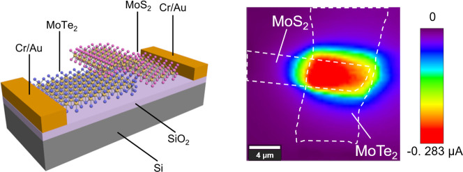
To identify the spatial distribution of the photocurrent generation, photocurrent mapping was performed, as shown in Figure 4. The laser beam scans the device with a uniform velocity in the designated area, and the photocurrent is recorded using a Raman Witec 300R system. Photocurrent mapping of the device was performed under λ = 532 nm (P = 350 μW, Vds = 0 V) and λ = 1064 nm (P = 180 μW, Vds = 0 V) illumination, and the diameter of the laser spot is estimated to be 0.5 μm. The red part in Figure 4, which represents a large photocurrent, is the area where MoTe2 and MoS2 overlapped, corresponding to the optical image of the MoTe2–MoS2 device. However, the photocurrent is not uniformly distributed in the heterojunction. This can be explained by the nonuniform contacts between the MoTe2 and MoS2. The maximum illumination current Iillum is detected to be −0.283 and −0.055 μA with the laser wavelength λ = 532 and λ = 1064 nm, respectively. When Vds < 0 V, similar photocurrent distribution was observed in the same device (See in Figure S4). The p–n junction formed by MoTe2 and MoS2 exhibits good characteristics. Obviously, the separation of photogenerated carriers and the dominant part of photocurrent occur in the overlapped area.
Figure 4.
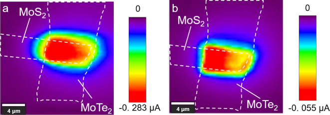
Spatial distribution of the photocurrent at Vds = 0 V. (a) λ = 532 nm. (b) λ = 1064 nm.
The comparison of MoTe2–MoS2 photodetector parameters is given in Table 1, including the thickness of the material, wavelength of illumination, bias voltage, and photoresponsivity. It is evident that the device we produced possesses comparable photodetection responsivity.
Table 1. Comparison of the Photodetector Parameters Based on MoTe2–MoS2 Heterostructure Devices.
Conclusions
In summary, we demonstrated a MoTe2–MoS2 heterostructure device with excellent characteristics. The heterostructure device exhibited rectification characteristics, indicating good formation of the p–n junction, and the I–V characteristics under the illumination of different laser (λ = 532 nm and 1064 nm) powers were measured. The heterostructure device achieved high-performance photodetection under Vds ≤ 0 V, and the photocurrent was generated at the overlapped area. These excellent performances illustrate that 2D van der Waals heterojunctions have prospective potentials in nanoscale optoelectronics.
Experimental Section
Device Fabrication
The MoTe2–MoS2 device was fabricated using the mechanical exfoliation method and restack technique. MoTe2 flakes were exfoliated using Scotch tape and transferred onto 290 nm SiO2/Si substrates. The MoS2 flakes were exfoliated using Scotch tape and transferred onto polydimethylsiloxane (PDMS). Then, we used the two-dimensional material transfer platform (Onway Technology) to accurately transfer MoS2 (on the PDMS substrate) to MoTe2 (on the Si/SiO2 substrate). The optical image was obtained using an optical microscope. The electrodes were patterned using a UV lithography system (TuoTuo Technology) or electron beam lithography (Raith Eline Plus). The electrode preparation of MoTe2 and MoS2 was completed by magneto-controlled sputtering. The corresponding electrode is 5 nm Cr/50 nm Au. Then, we put the sample in 60 °C acetone for lift-off, and we used an ultrasonic wire bonding machine to complete the device bonding.
Electrical and Photoelectrical Measurements
The Raman single-point spectrum and Raman scanning area mapping were characterized using a Raman Witec 300R system with an excitation laser of λ = 532 nm. Electrical and photoelectrical characteristic measurements of the MoTe2–MoS2 device were conducted using a source meter (Keithley 2636B). The diameter of the laser spot is about 0.5 μm, and photocurrent mapping was characterized using a Raman Witec 300R system in the Raman photocurrent mode.
Acknowledgments
This work is financially supported by the National Key R&D Program of China (no. 2018YFA0306900) and the Natural Science Foundation of Hunan Province (no. 2020JJ3039, 2020JJ4659, and 2020RC3032).
Supporting Information Available
The Supporting Information is available free of charge at https://pubs.acs.org/doi/10.1021/acsomega.1c06009.
AFM morphology image of the MoTe2–MoS2 heterostructure, characterizations of the MoTe2–MoS2 heterostructures device, I–V curve of the MoTe2–MoS2 heterostructures device before annealing, and spatial distribution of the photocurrent (PDF)
Author Contributions
X.J. fabricated all the devices and performed all the characterizations and measurements; Z.B. helped to build the van der Waals heterostructures; F.L. helped to fabricate the devices; Z.Z. built a home-built optics system and opto-electronic system. C.G., M.Z., and S.Q. supervised this project. X.J. and M.Z. wrote the article with the help of all authors. All authors have given approval to the final version of the article.
The authors declare no competing financial interest.
Supplementary Material
References
- Wang J.; Fang H.; Wang X.; Chen X.; Lu W.; Hu W. Recent Progress on Localized Field Enhanced Two-dimensional Material Photodetectors from Ultraviolet-Visible to Infrared. Small 2017, 13, 1700894. 10.1002/smll.201700894. [DOI] [PubMed] [Google Scholar]
- Wang P.; Xia H.; Li Q.; Wang F.; Zhang L.; Li T.; Martyniuk P.; Rogalski A.; Hu W. Sensing Infrared Photons at Room Temperature: From Bulk Materials to Atomic Layers. Small 2019, 15, 1904396. 10.1002/smll.201904396. [DOI] [PubMed] [Google Scholar]
- Wang F.; Zhang Y.; Gao Y.; Luo P.; Su J.; Han W.; Liu K.; Li H.; Zhai T. 2D Metal Chalcogenides for IR Photodetection. Small 2019, 15, 1901347. 10.1002/smll.201901347. [DOI] [PubMed] [Google Scholar]
- Chen H.; Liu H.; Zhang Z.; Hu K.; Fang X. Nanostructured Photodetectors: From Ultraviolet to Terahertz. Adv. Mater. 2016, 28, 403–433. 10.1002/adma.201503534. [DOI] [PubMed] [Google Scholar]
- Lussani F. C.; Vescovi R. F. d. C.; Souza T. D. d.; Leite C. A. P.; Giles C. A versatile x-ray microtomography station for biomedical imaging and materials research. Rev. Sci. Instrum. 2015, 86, 063705. 10.1063/1.4922607. [DOI] [PubMed] [Google Scholar]
- Wu J.; Lu Y.; Feng S.; Wu Z.; Lin S.; Hao Z.; Yao T.; Li X.; Zhu H.; Lin S. The Interaction between Quantum Dots and Graphene: The Applications in Graphene-Based Solar Cells and Photodetectors. Adv. Funct. Mater. 2018, 28, 1804712. 10.1002/adfm.201804712. [DOI] [Google Scholar]
- Wang X.; Shen H.; Chen Y.; Wu G.; Wang P.; Xia H.; Lin T.; Zhou P.; Hu W.; Meng X.; Chu J.; Wang J. Multimechanism Synergistic Photodetectors with Ultrabroad Spectrum Response from 375 nm to 10 μm. Adv. Sci. 2019, 6, 1901050. 10.1002/advs.201901050. [DOI] [PMC free article] [PubMed] [Google Scholar]
- Lin C.-H.; Anselm A.; Kuo C.-H.; Delaney A. M.; Brown G. J.; Mahalingam K.; Saxler A. W.; Linville R. J.; Szmulowicz F.; Nathan V. Type II InAs/InGaSb SL photodetectors. Proc. SPIE-Int. Soc. Opt. Eng. 2000, 3948, 133–144. 10.1117/12.382112. [DOI] [Google Scholar]
- Rogalski A. HgCdTe infrared detector material: history, status and outlook. Rep. Prog. Phys. 2005, 68, 2267–2336. 10.1088/0034-4885/68/10/r01. [DOI] [Google Scholar]
- Tan C.; Cao X.; Wu X.-J.; He Q.; Yang J.; Zhang X.; Chen J.; Zhao W.; Han S.; Nam G.-H.; Sindoro M.; Zhang H. Recent Advances in Ultrathin Two-Dimensional Nanomaterials. Chem. Rev. 2017, 117, 6225–6331. 10.1021/acs.chemrev.6b00558. [DOI] [PubMed] [Google Scholar]
- Jariwala D.; Marks T. J.; Hersam M. C. Mixed-dimensional van der Waals heterostructures. Nat. Mater. 2017, 16, 170–181. 10.1038/nmat4703. [DOI] [PubMed] [Google Scholar]
- Miró P.; Audiffred M.; Heine T. An atlas of two-dimensional materials. Chem. Soc. Rev. 2014, 43, 6537–6554. 10.1039/c4cs00102h. [DOI] [PubMed] [Google Scholar]
- Long M.; Wang P.; Fang H.; Hu W. Progress, Challenges, and Opportunities for 2D Material Based Photodetectors. Adv. Funct. Mater. 2019, 29, 1803807. 10.1002/adfm.201803807. [DOI] [Google Scholar]
- Zhang J.; Lyu J.; Ni Z. Highly sensitive infrared detector based on a two-dimensional heterojunction. Chin. Opt. 2021, 14, 87–99. 10.37188/CO.2020-0139. [DOI] [Google Scholar]
- Zhang K.; Zhang T.; Cheng G.; Li T.; Wang S.; Wei W.; Zhou X.; Yu W.; Sun Y.; Wang P.; Zhang D.; Zeng C.; Wang X.; Hu W.; Fan H. J.; Shen G.; Chen X.; Duan X.; Chang K.; Dai N. Interlayer Transition and Infrared Photodetection in Atomically Thin Type-II MoTe2/MoS2 van der Waals Heterostructures. ACS Nano 2016, 10, 3852–3858. 10.1021/acsnano.6b00980. [DOI] [PubMed] [Google Scholar]
- Radisavljevic B.; Radenovic A.; Brivio J.; Giacometti V.; Kis A. Single-layer MoS2 transistors. Nat. Nanotechnol. 2011, 6, 147–150. 10.1038/nnano.2010.279. [DOI] [PubMed] [Google Scholar]
- Huang H.; Wang J.; Hu W.; Liao L.; Wang P.; Wang X.; Gong F.; Chen Y.; Wu G.; Luo W.; Shen H.; Lin T.; Sun J.; Meng X.; Chen X.; Chu J. Highly sensitive visible to infrared MoTe2 photodetectors enhanced by the photogating effect. Nanotechnology 2016, 27, 445201. 10.1088/0957-4484/27/44/445201. [DOI] [PubMed] [Google Scholar]
- Chen Y.; Wang X.; Wang P.; Huang H.; Wu G.; Tian B.; Hong Z.; Wang Y.; Sun S.; Shen H.; Wang J.; Hu W.; Sun J.; Meng X.; Chu J. Optoelectronic Properties of Few-Layer MoS2 FET Gated by Ferroelectric Relaxor Polymer. ACS Appl. Mater. Interfaces 2016, 8, 32083–32088. 10.1021/acsami.6b10206. [DOI] [PubMed] [Google Scholar]
- Ruppert C.; Aslan O. B.; Heinz T. F. Optical properties and band gap of single- and few-layer MoTe2 crystals. Nano Lett. 2014, 14, 6231–6236. 10.1021/nl502557g. [DOI] [PubMed] [Google Scholar]
- Li H.; Zhang Q.; Yap C. C. R.; Tay B. K.; Edwin T. H. T.; Olivier A.; Baillargeat D. From Bulk to Monolayer MoS2: Evolution of Raman Scattering. Adv. Funct. Mater. 2012, 22, 1385–1390. 10.1002/adfm.201102111. [DOI] [Google Scholar]
- Chen Y.; Wang X.; Wu G.; Wang Z.; Fang H.; Lin T.; Sun S.; Shen H.; Hu W.; Wang J.; Sun J.; Meng X.; Chu J. High-Performance Photovoltaic Detector Based on MoTe2/MoS2 van der Waals Heterostructure. Small 2018, 14, 1703293. 10.1002/smll.201703293. [DOI] [PubMed] [Google Scholar]
- Deng Y.; Luo Z.; Conrad N. J.; Liu H.; Gong Y.; Najmaei S.; Ajayan P. M.; Lou J.; Xu X.; Ye P. D. Black phosphorus-monolayer MoS2 van der Waals heterojunction p-n diode. ACS Nano 2014, 8, 8292–8299. 10.1021/nn5027388. [DOI] [PubMed] [Google Scholar]
- Peng M.; Xie R.; Wang Z.; Wang P.; Wang F.; Ge H.; Wang Y.; Zhong F.; Wu P.; Ye J.; Li Q.; Zhang L.; Ge X.; Ye Y.; Lei Y.; Jiang W.; Hu Z.; Wu F.; Zhou X.; Miao J.; Wang J.; Yan H.; Shan C.; Dai J.; Chen C.; Chen X.; Lu W.; Hu W. Blackbody-sensitive room-temperature infrared photodetectors based on low-dimensional tellurium grown by chemical vapor deposition. Sci. Adv. 2021, 7, eabf7358 10.1126/sciadv.abf7358. [DOI] [PMC free article] [PubMed] [Google Scholar]
- Chen Y.; Wang Y.; Wang Z.; Gu Y.; Ye Y.; Chai X.; Ye J.; Chen Y.; Xie R.; Zhou Y.; Hu Z.; Li Q.; Zhang L.; Wang F.; Wang P.; Miao J.; Wang J.; Chen X.; Lu W.; Zhou P.; Hu W. Unipolar barrier photodetectors based on van der Waals heterostructures. Nat. Electron. 2021, 4, 357–363. 10.1038/s41928-021-00586-w. [DOI] [Google Scholar]
- Wu F.; Li Q.; Wang P.; Xia H.; Wang Z.; Wang Y.; Luo M.; Chen L.; Chen F.; Miao J.; Chen X.; Lu W.; Shan C.; Pan A.; Wu X.; Ren W.; Jariwala D.; Hu W. High efficiency and fast van der Waals hetero-photodiodes with a unilateral depletion region. Nat. Commun. 2019, 10, 4663. 10.1038/s41467-019-12707-3. [DOI] [PMC free article] [PubMed] [Google Scholar]
- Hu S.; Tian R.; Gan X. Two-dimensional material photodetector for hybrid silicon photonics. Chin. Opt. 2021, 14, 1039–1055. [Google Scholar]
- Wang F.; Yin L.; Wang Z. X.; Xu K.; Wang F. M.; Shifa T. A.; Huang Y.; Jiang C.; He J. Configuration-Dependent Electrically Tunable van der Waals Heterostructures Based on MoTe2/MoS2. Adv. Funct. Mater. 2016, 26, 5499–5506. 10.1002/adfm.201601349. [DOI] [Google Scholar]
- Wang B.; Yang S.; Wang C.; Wu M.; Huang L.; Liu Q.; Jiang C. Enhanced current rectification and self-powered photoresponse in multilayer p-MoTe2/n-MoS2 van der Waals heterojunctions. Nanoscale 2017, 9, 10733–10740. 10.1039/c7nr03445h. [DOI] [PubMed] [Google Scholar]
- Pezeshki A.; Shokouh S. H. H.; Nazari T.; Oh K.; Im S. Electric and Photovoltaic Behavior of a Few-Layer alpha-MoTe2/MoS2 Dichalcogenide Heterojunction. Adv. Mater. 2016, 28, 3216–3222. 10.1002/adma.201504090. [DOI] [PubMed] [Google Scholar]
Associated Data
This section collects any data citations, data availability statements, or supplementary materials included in this article.


