Abstract
Electronic waste can lead to the accumulation of environmentally and biologically toxic materials and is a growing global concern. Developments in transient electronics—in which devices are designed to disintegrate after use—have focused on increasing the biocompatibility, whereas efforts to develop methods to recapture and reuse materials have focused on conducting materials, while neglecting other electronic materials. Here, we report all-carbon thin-film transistors made using crystalline nanocellulose as a dielectric, carbon nanotubes as a semiconductor, graphene as a conductor and paper as a substrate. A crystalline nanocellulose ink is developed that is compatible with nanotube and graphene inks and can be written onto a paper substrate using room-temperature aerosol jet printing. The addition of mobile sodium ions to the dielectric improves the thin-film transistor on-current (87 μA mm−1) and subthreshold swing (132 mV dec−1), and leads to a faster voltage sweep rate (by around 20 times) than without ions. The devices also exhibit stable performance over six months in ambient conditions and can be controllably decomposed, with the graphene and carbon nanotube inks recaptured for recycling (>95% recapture efficiency) and reprinting of new transistors. We demonstrate the utility of the thin-film transistors by creating a fully printed, paper-based biosensor for lactate sensing.
Electronic waste (e-waste) is one of the fastest growing waste streams in the world1, introducing high levels of toxic pollutants to the environment. Transient electronics2—where devices are designed to controllably disintegrate after use—have been proposed as a way to decrease the ecological and health impacts of e-waste. However, the approach, which has been largely used in biologically integrated sensors3 and therapeutics4, still leads to the accumulation of silicon-based materials and carbon-nanostructured waste, which are themselves e-waste5. Fully recyclable electronics, in which environmentally and biologically damaging components are recaptured and reused, thus remains the goal.
Efforts to develop recyclable electronics have focused on the recapture of liquid-metal conductive traces6 or the degradation of a single component7. A unified system that considers all components would have a more substantial environmental impact. Furthermore, recyclable electronics that require high temperatures during manufacture can still have elevated energy costs and environmentally damaging processing conditions8, which could be substantially reduced by, for example, printing at room temperature9.
One promising approach for printable, recyclable electronics is to use all-carbon components10. Both semiconducting carbon nanotubes (CNTs) and conducting graphene have long been explored for printed electronics11,12, and cellulose has previously been used as a substrate13 and dielectric14. (Cellulose is completely biodegradable and the most abundant biopolymer on earth, making it relatively inexpensive15.) However, owing to an absence of solution-processable carbon-based dielectrics, achievements in all-carbon printed electronics remain limited, with previous demonstrations incorporating inorganic components16–18. Cellulose paper has been shown to work as a dielectric in high-power transformers19, but crystalline nanocellulose has typically been used as a binder or in tandem with a high-k dielectric15,20, not as a standalone printable dielectric.
In this Article, we report all-carbon recyclable electronics created using a crystalline nanocellulose dielectric ink that is printable at room temperature and with compatible CNT and graphene inks. The inks can be directly written onto a paper substrate using room-temperature aerosol jet printing. We use the nanocellulose ink to fabricate all-carbon thin-film transistors (TFTs) in which all the constituents can either be recaptured and reused as reclaimed inks (CNTs, graphene), or degrade completely (cellulose). The dielectric performance of the crystalline nanocellulose was improved by the addition of 0.15 mM sodium chloride (NaCl) to the aqueous ink, leading to higher transistor sweep rates (~600 mV s−1), a lowered subthreshold swing (SS, 132 mV dec−1) and higher on-current (87 µA mm−1). The devices also exhibit stable performance over six months in ambient conditions. To illustrate the capabilities of our all-carbon electronics, the TFTs are used to create a fully-printed, paper-based biosensor for lactate sensing, which shows a concentration sensitivity range relevant for diagnosis of septic shock (>2 mM).
Crystalline nanocellulose printing
We first examined the use of crystalline nanocellulose (Fig. 1a) as a standalone printed dielectric. The relationship between dynamic viscosity and nanocellulose concentration in water displayed evidence of shear-thinning behaviour across all concentrations, with viscosities ranging across two orders of magnitude. Furthermore, nanocellulose and graphene inks maintained viscosities orders of magnitude greater than water at low shear rates (Fig. 1b and Extended Data Fig. 1). Aerosol jet printing, which uses ultrasonication of ink to create a suspension of ink constituents in 1–5-µm droplets (Fig. 1c,d), is therefore an ideal direct-write deposition method as it allows for the printing of higher-viscosity fluids21 compared to inkjet printing22. A sufficiently high flow rate and concentration are needed to form monolithic films that can effectively insulate electric charge (Fig. 1e,f). At low concentrations and flow rates, deposited microdroplets will evaporate too rapidly to make a coherent film and hence will form a porous structure. With very few exceptions23, printable dielectrics require elevated post-processing temperatures to exhibit desirable insulating behaviour24. However, the crystalline nanocellulose films were printed at room temperature without observable performance degradation (Supplementary Fig. 1).
Fig. 1 |. Nanocellulose printing.
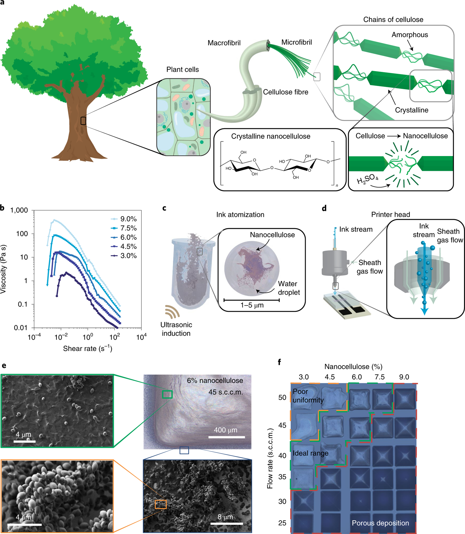
a, Schematic of the hierarchical structure of crystalline nanocellulose. b, Dynamic viscosity plotted versus shear rate for a range of nanocellulose concentrations in water. c, Schematic of the aerosol jet printing ultrasonication process, with a magnified view of an ink droplet. d, Schematic of the printer head with a magnified view of the printer nozzle. e, Scanning electron microscope (SEM) images of a printed nanocellulose film at various magnifications compared to an optical image. f, Grid of printed nanocellulose squares as a function of flow rate (measured in standard cubic centimetres per minute, s.c.c.m.) and nanocellulose concentration.
All-carbon printed transistors
Using this crystalline nanocellulose dielectric ink, all-carbon TFTs were printed on a paper substrate with graphene source/drain/gate electrodes and a CNT channel (Fig. 2a and Extended Data Fig. 2). Briefly, a graphene source and drain were printed on photograph paper, then a CNT channel was printed and rinsed in an 80 °C toluene bath for 10 min. After the substrate was dried, a nanocellulose dielectric was printed to cover the source and drain electrodes, then a graphene top gate was printed on top of the nanocellulose to cover the channel region. Previous reports claiming ‘all-carbon’ electronics in fact incorporate inorganic components, focusing only on a carbonaceous channel and electrodes16–18, whereas the printed nanocellulose gate dielectric in our TFTs yields a fully all-carbon device. The nanocellulose films exhibit frequency-dependent dielectric behaviour consistent with ion-gel or electrolyte dielectrics, facilitated by absorbed water, which mobilizes ions in the film to yield a double-layer capacitance (Extended Data Figs. 3 and 4)25. Ion gels generally provide increased freedom in transistor gate placement, so this part of the design is often overlooked in favour of simple side-gated arrangements to reduce fabrication complexity. However, we discovered a gate position-dependent modulation of the channel charge for the all-carbon TFTs, as shown in a surface map of the transistor’s on-current/off-current ratio (log(Ion/Ioff)) versus gate probe tip position (Fig. 2b,c). Unlike ion-gel dielectrics, almost no switching behaviour is observed far away from the channel, so a top-gated structure is critical in these devices.
Fig. 2 |. All-carbon TFT printing and testing.
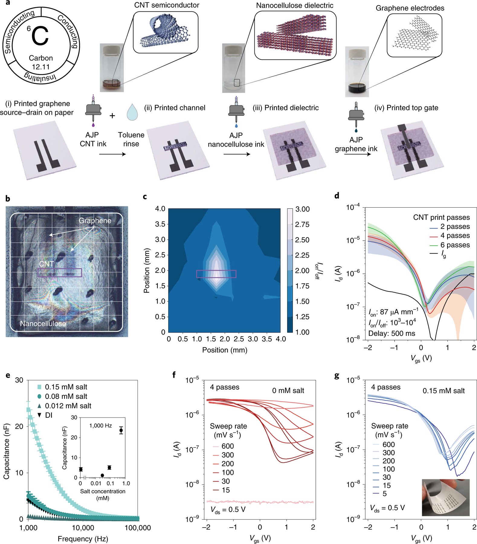
a, printing fabrication schematic with all-carbon inks. AJp, aerosol jet printing. b, Top-view optical image of the all-carbon TFT without a printed top gate. c, Surface map of transistor Ion/Ioff as a function of gating location (determined by probe placement on the nanocellulose thin film) for the TFT in b. d, Subthreshold curves as a function of CNT print passes. The data represent the average value (line) ± standard deviation (shaded region) of 12 devices without added salt at a Vds of −0.5 V. e, Frequency-dependent capacitance versus ink salt concentration (with values at 1,000 Hz shown in the inset). f,g, Subthreshold curves measured with different sweep rates for devices with no added salt (f) and with 0.15 mM NaCl added (g) to the nanocellulose ink, which yields robust switching even with a 600 mV s−1 sweep rate. The inset in g is a photograph of an array of all-carbon transistors. All devices in this report have a channel length of 250 μm and a channel width of 200 μm.
The impact of CNT film density was investigated for the all-carbon TFTs with two, four and six printing passes of CNT ink (Fig. 2d). All processing was performed at room temperature, except for a 10-min toluene soak at 80 °C after nanotube printing. Although previous reports26 indicated promising performance with a lower density of aerosol-jet-printed CNTs, four passes of CNT ink provided transistors with optimal performance, demonstrating an Ion/Ioff ratio of 103–104, Ion of 87.00 ± 18.25 µA mm−1 and SS of 132 ± 70 mV dec−1 (Extended Data Fig. 5). Tolerance to increased CNT density is attributed to the higher roughness of photograph paper compared to a silicon surface.
Because the performance of ionic-based dielectrics depends on the diffusion of ions to establish a double layer of charge (Extended Data Fig. 6), the switching speed is traditionally slower than that of solid-state dielectrics27. This is observed in the frequency-dependent capacitance (Fig. 2e) and the transistor switching dependence on the gate voltage sweep rate (Fig. 2f)—the rate at which voltage is changed (mV s−1) based on adjustment of the hold time for each voltage step. Almost no modulation is observed at a sweep rate of ~600 mV s−1, with an Ion/Ioff ratio of 1.5, whereas the transistor behaves as expected at a sweep rate of ~30 mV s−1, with an Ion/Ioff of 66.1.
This frequency-dependent behaviour indicates limited ionic mobility, which is ultimately determined by the ion source in the dielectric. Nanocellulose is produced by acid hydrolysis of cellulose, a process that sulfonates the cellulose, leaving it charged28. To confirm this, the addition of 0.012 mM salt to the ink solution (Extended Data Fig. 7) was shown to screen the crystalline nanocellulose surface charge and nearly eliminate the frequency-dependent capacitance (Fig. 2e and insert). Given that the surface charge is bonded to the crystalline nanocellulose backbone, ion mobility is minimal and the device requires slow sweep rates to operate. Once this surface charge is screened, any added salt ions function as highly mobile carriers, improving device responsiveness. The addition of 0.15 mM NaCl almost entirely eliminates the dependence on sweep rate (Fig. 2g). Although the device performance is still dependent on ion mobility, only a 21% decrease in Ion/Ioff is observed when the sweep rate is increased from ~30 mV s−1 to ~600 mV s−1, as opposed to a 98% decrease without the addition of the mobile ions.
Although the off-current of these all-carbon TFTs remains relatively high compared to high-performance TFTs, the on-current and switching behaviour of these printed devices are among the highest for printed transistors (of any material) and especially for printed transistors on paper (Fig. 3; data taken from Supplementary Table 1). In particular, the relatively high on-current at low voltages (87 μA mm−1 at a Vds of −0.5 V), in spite of the high surface roughness of the paper substrate (which impacts thin-film deposition uniformity), makes these TFTs ideal for scenarios that require portable, moderate-performance devices. To demonstrate the applied sensing utility of this all-carbon, recyclable platform, a fully printed, paper-based biosensor from an extended gate TFT for lactate sensing was fabricated and shown to yield an expanded measurement range (compared to a simple two-electrode device), reaching concentrations relevant for the medical diagnosis of sepsis (>2 mM) (Extended Data Fig. 8).
Fig. 3 |. Benchmarking printed all-carbon TFT performance against other printed transistors.
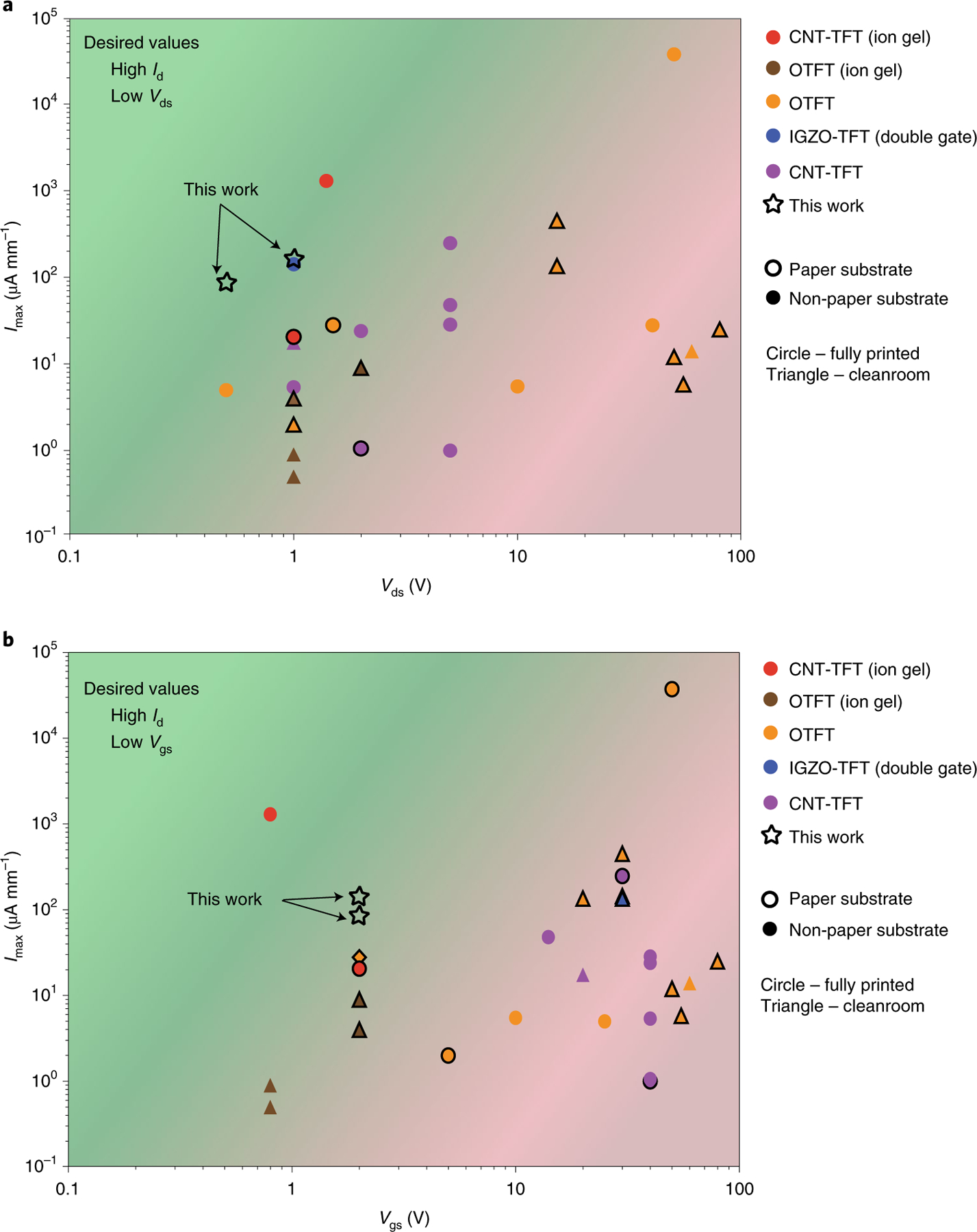
a, Width-normalized on-current plotted against drain–source voltage for different TFTs. b, Width-normalized on-current plotted against gate voltage. Colours represent transistor types (both semiconducting material and gating scheme). CNT-TFTs use a semiconducting CNT channel, organic TFTs (OTFTs) use an organic semiconductor channel and iGZO is indium gallium zinc oxide. ion-gel-based transistors use a solid electrolyte as the dielectric. Shapes represent processing technique, with circles indicating fully printed transistors and triangles representing transistors that utilize cleanroom techniques in at least some of the processing. Finally, data points with a border are transistors on a paper substrate. Data for other TFTs can be found in Supplementary Table 1.
Recycling printed nanomaterials
The all-carbon inks allow for the development of printed all-carbon recyclable electronics (Fig. 4a). Whereas many physically transient devices degrade over the course of use2, the all-carbon, recyclable transistors presented here exhibit high stability when stored in ambient conditions over the course of six months (Fig. 4b). Once their utility is exhausted (for example, after use in biosensing), the components can be controllably broken down and the inks recycled for later reuse. Previously reported components show notable performance alterations upon recycling29, or recycle only the conductive trace4 or substrate30. Ultrasonic recycling of our all-carbon TFTs produced inks nearly indistinguishable from the original CNT ink (Fig. 4c–e) and functional, although less conductive, graphene ink (Fig. 3f). Five iterations of CNT and graphene ink recycling demonstrated average recovery yields of 95 ± 6% and 98 ± 5%, respectively (Extended Data Fig. 9). Furthermore, we reprinted the recycled CNTs into transistors that showed nearly identical performance to the TFTs created from new ink (Fig. 4f). The slight decrease in on-current is attributed to the decreased CNT ink concentration and thus lower printed CNT density (Extended Data Fig. 10) and is commensurate with batch-to-batch variations observed even with new inks. Fully recycled TFTs (printed with recycled CNT and graphene inks) showed only a minimal decrease in on-current, attributed to the lower conductivity of the recycled graphene that may stem from increased bundling in the graphene ink and might be improved through reformulation of the recycled ink.
Fig. 4 |. All-carbon TFTs with demonstration of controlled recycling.
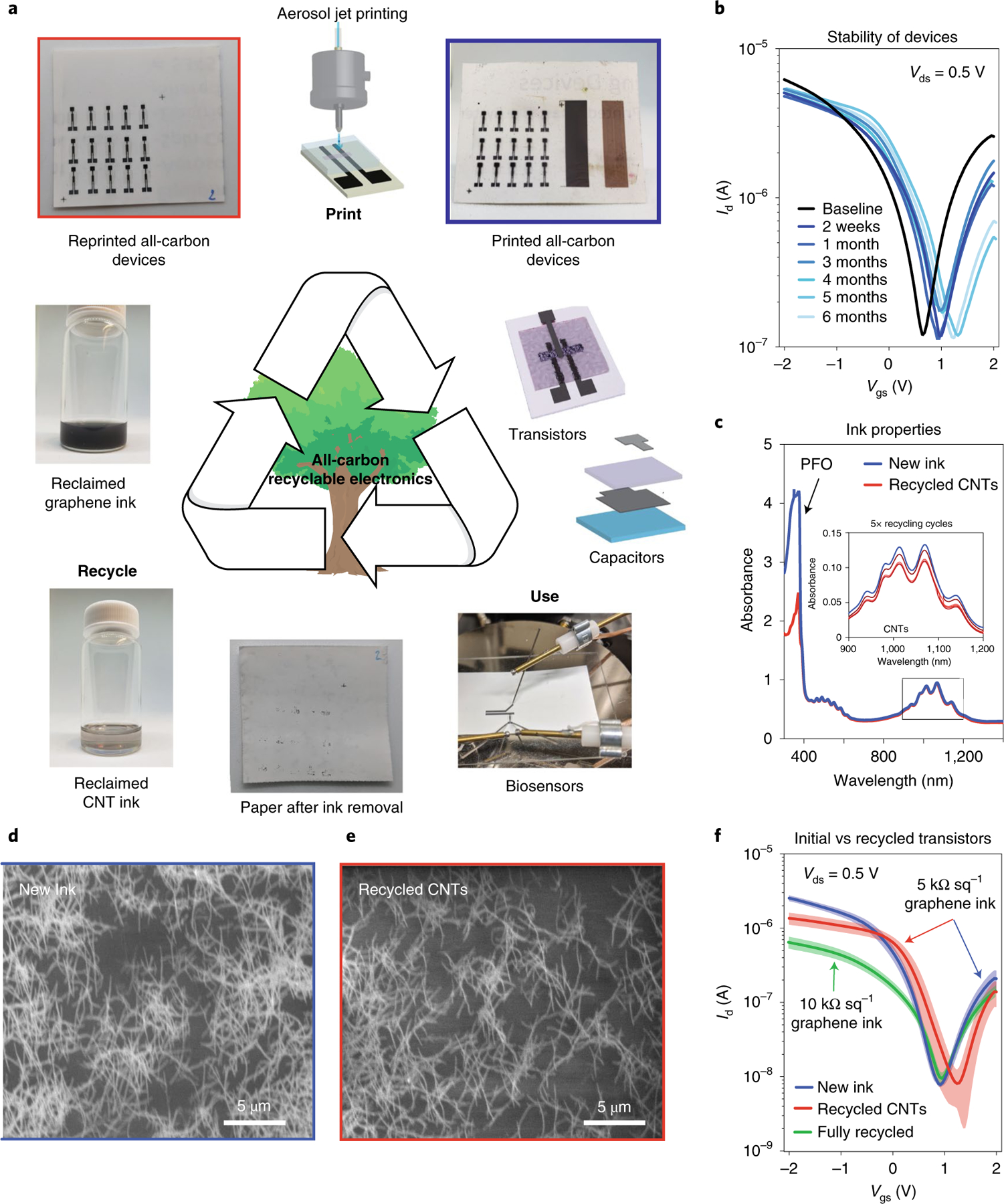
a, Schematic of the all-carbon recyclable electronics system, demonstrating printing, use (see Extended Data Fig. 8 for a biosensing demonstration) and recycling, then reprinting, reuse and so on. The top right inset shows an array of all-carbon recyclable electronic TFTs with excess graphene (left) and CNTs (right) printed to the side. b, Stable TFT characteristics over six months of storage in air. The transistor was fabricated without salt and run with a sweep rate of ~30 mV s−1. c, UV–vis–Nir spectra of new ink and five iterations of CNT ink recycling, showing minimal loss in ink concentration over the five recycling cycles. d,e, SEM images of printed new (d) and recycled (e) CNT inks. f, Subthreshold curves of transistors from new and recycled inks, with nominally consistent performance using recycled CNTs and slight reduction with recycled CNTs and graphene due to the increased graphene sheet resistance (attributed to increased bundling in the recycled ink). The data represent average ± standard deviation of four devices with a salt concentration of 0.15 mM in the nanocellulose and a sweep rate of ~600 mV s−1.
Conclusions
We have reported the development of a crystalline nanocellulose ink that can form films with frequency-independent dielectric behaviour for use as a gate dielectric that is printable at room temperature. Together with CNT and graphene inks, the nanocellulose ink was used to create fully printed and recyclable all-carbon TFTs on paper. The resulting transistors exhibit on/off-current ratios of 104, SS of 130 mV dec−1 and on-current of 87 μA mm−1. The all-carbon devices are air-stable, and their constituent materials can be recycled for further use, mitigating the potential environmental impact over the device life cycle. We also showed that the transistors can be used to create a lactate biosensor. Our platform offers an environmentally friendly approach to printing custom electronic devices for use in the expanding internet-of-everything.
Methods
Materials.
Crystalline nanocellulose (CNC-Slurry) was purchased from Cellulose Lab at a concentration of 12% solids. To prepare the ink for printing, crystalline nanocellulose was diluted in water to concentrations ranging from 3 to 9% (wt/wt) crystalline nanocellulose. Sodium chloride (>99.0% ACS reagent grade) was purchased from Sigma-Aldrich. Semiconducting CNTs (IsoSol-S100 polymer-wrapped nanotubes) were purchased from NanoIntegris. To prepare the ink for printing, the vial of as-purchased ink was ultrasonicated for 30 min to redisperse the CNTs. The ink was diluted to a concentration of 0.05 mg ml−1 in toluene for printing. Graphene ink (805556–10ML) was purchased from Sigma-Aldrich. The ink was diluted to one-third the initial concentration in deionized (DI) water for printing. Paper (gloss white) was purchased from FedEx and used as is. Phosphate buffered saline (1×PBS) was purchased from Sigma-Aldrich and used as is. Lactate oxidase (LOx) powder (L9795) was purchased from Sigma-Aldrich. The powder was mixed with 1×PBS to achieve a concentration of 200 U ml−1 and vortexed for 5 min to dissolve. A 50-µl volume of the protein was distributed into Eppendorf flasks and flash-frozen in liquid nitrogen. The protein was thawed by placing one Eppendorf flask in an ice water bath, as a slower thaw reduces the risk of LOx denaturization. Sodium l-lactate was purchased from Sigma-Aldrich and concentrated to 10 mM in 1×PBS. Silver nanowires (AgNW) of length ~4 μm were synthesized using the method described in a previous publication31, and suspended in DI water at a concentration of 10 mg ml−1 with the addition of 0.01% (wt/wt) hydroxypropyl methyl cellulose as a viscosity enhancer to enable printing of high-fidelity conductive traces at room temperature.
Aerosol jet printing.
All printing was performed on an AJ-300 printer (Optomec) with the platen temperature at room temperature and the ink held at a constant 20 °C throughout printing.
Graphene printing.
A 150-µm-diameter nozzle was used to print all graphene traces and films with a print speed of 2 mm s−1. A sheath flow rate of 25 s.c.c.m., an atomizer flow rate of 40–50 s.c.c.m. and an ultrasonic inducer current of 340–350 mA were used. One pass of graphene ink was used in all prints with new ink and four print passes were used for the recycled graphene ink due to modifications such as concentration and polymer fraction that resulted in higher resistance of the resulting ink (note: these should be addressable through reformulation of the recycled ink to match that of the new ink). As soon as a coherent line was observed, printing was initiated.
Semiconducting CNT printing.
A 150-µm-diameter nozzle was used to print all CNT films with a print speed of 2 mm s−1. A sheath flow rate of 40 s.c.c.m., an atomizer flow rate of 23 s.c.c.m. and an ultrasonic inducer current of 340–350 mA were used. Two to six passes of CNT ink were used for all prints. The ink temperature was allowed to equilibrate in the printer under ultrasonication for 30 min before the atomizer flow was initiated to ensure that all components of the atomizer impactor reached thermal equilibrium, which increases print uniformity, as described in a previous publication32. CNT flow was allowed to stabilize for 10 min before initial printing commenced. Subsequent printing passes proceeded without any additional requirements for stabilization periods.
Crystalline nanocellulose printing.
A 300-µm-diameter nozzle was used to print all crystalline nanocellulose films with a print speed of 5 mm s−1. A sheath flow rate of 23 s.c.c.m., an atomizer flow rate of 45 s.c.c.m. and an ultrasonic inducer current of 340–350 mA were used. One pass of crystalline nanocellulose ink was used for all prints. As soon as a coherent line without excessive overspray was observed, printing was initiated.
AgNW printing.
A 150-µm-diameter nozzle was used to print the AgNW films with a print speed of 1 mm s−1. A sheath flow rate of 23 s.c.c.m., an atomizer flow rate of 45 s.c.c.m. and an ultrasonic inducer current of 340–350 mA were used. Three total passes were used to enhance the conductivity.
Capacitor fabrication.
The capacitors were fabricated on glass substrates. To prepare the substrate, the glass slide was first ultrasonicated in isopropyl alcohol (IPA) for 10 min, rinsed with DI water, and dried with nitrogen (N2), then ultrasonicated in acetone for 10 min, rinsed with DI water, and dried with N2. A 30-nm layer of gold was evaporated using a CHA Industries Solution E-Beam evaporator for the bottom electrode. Nanocellulose was then printed as the dielectric using the above parameters. Finally, AgNWs were printed as the top electrode using the above parameters.
Transistor fabrication.
To print the all-carbon transistors, a piece of photograph paper was placed onto the aerosol jet printer platen. Source and drain electrodes were printed using graphene ink using the above parameters, then, without removal of the substrate from the platen, the CNT channel was printed using the above parameters. After CNT printing, the substrate was soaked in a toluene bath for 10 min at 80 °C to remove excess polydioctylfluorene. This process is required to achieve a sufficiently conductive transistor channel. (Note that other reports have demonstrated that this polymer-removal process is also feasible using a toluene rinse without removing the substrate from the printer platen, as long as the platen is held at an elevated temperature (80 °C).) The substrate was then placed back on the printer platen and the crystalline nanocellulose ionic dielectric was printed using the above parameters. Finally, without further removal of the substrate from the printer platen, a graphene gate was printed on top of the nanocellulose. All devices in this report have a channel length of 250 μm and a channel width of 200 μm.
Lactate sensor fabrication.
To print the all-carbon lactate sensor, a piece of photograph paper was placed onto the aerosol jet printer platen. For the two-electrode sensor, graphene working and common electrodes were printed using the above parameters. For the transistor-based sensor, source and drain electrodes were first printed using graphene ink using the above parameters, then, without removal of the substrate from the platen, the CNT channel was printed using the above parameters. After CNT printing, the substrate was soaked in a toluene bath for 10 min at 80 °C. The substrate was then placed back on the printer platen and the crystalline nanocellulose dielectric was printed using the above parameters. Without further removal of the substrate from the printer platen, a graphene working and common electrode were printed to the side of the device. Finally, a gate connected to the working electrode was printed on top of the channel.
Lactate concentration testing.
All testing was performed on a Signatone H150W manual analytical probe station connected to an Agilent (Keysight Technologies) B-1500 semiconductor parameter analyser. For each test, 100 μl of 1×PBS was pipetted onto the paper substrate directly above the working and common electrodes. A 1-μl volume of LOx was pipetted into the PBS droplet and mixed 10 times with a pipette. A baseline measurement was taken. For the two-electrode measurement, the voltage across the working and common electrode was swept from –1 to 1 V and then back from 1 to –1 V. For the transistor measurement, the gate electrode was attached to the common electrode while the working electrode that was connected to the gate was allowed to float (Extended Data Fig. 8). During testing, the gate voltage was held at −0.5 V and the source–drain voltage was swept from −2 to 2 V. Varying concentrations of lactate were dosed into the PBS–LOx solution and mixed 10 times with a pipette. After lactate dosing and mixing, the solution was allowed to stabilize for 2 min before a voltage sweep was initiated for both the two-electrode and the transistor-based sensors.
Capacitor heat testing.
A baseline frequency sweep was performed on a Signatone H150W manual analytical probe station connected to an Agilent (Keysight Technologies) B-1500 semiconductor parameter analyser. The capacitors were then heated to a temperature of 80 °C on a hot plate for 1 h. After an hour, the capacitor was removed from the hot plate and a frequency–capacitance sweep was performed every 30 s for 30 min.
Capacitor vacuum testing.
Vacuum testing was performed using a cryogenic probe station (Lakeshore CRX-6.5K) in tandem with an Agilent (Keysight Technologies) B-1500 semiconductor parameter analyser. The capacitor was placed into the chamber and placed under a vacuum of 10−5 torr. The system was allowed 10 min to achieve a vacuum. At this point, the test was initiated. A frequency–capacitance sweep was performed every 30 s for the duration of the testing. After 12 min, the vacuum was purged and the top to the vacuum chamber was removed, exposing the capacitor to air. After 12 min in air, the top was replaced and the system was pumped down to a vacuum. Then, to test whether the increase in capacitance was due to pressure or atmosphere, the system was brought up to atmospheric pressure in nitrogen and held for 12 min, following by a 12-min hold in air with the vacuum chamber top removed. This was followed by a pump down, purge and pump down cycle, each 12-min long.
CNT printed density determination.
New and recycled inks were diluted to the same concentration (0.05 mg ml−1, assuming that 100% of all deposited ink was recaptured) and aerosol-jet-printed onto a silicon wafer with a 300-nm-thick thermally grown silicon dioxide insulator. The printing parameters for each were identical, with an atomizer flow rate of 40 s.c.c.m., a sheath flow rate of 23 s.c.c.m., an ultrasonic inducer current of 340–350 mA and a printer speed of 2 mm s−1. As with all CNT printing, the ink temperature was held at 20 °C to increase printing stability and each vial was allowed to reach thermal equilibrium with the ultrasonic bath for 30 min before the atomizer flow was initiated. An additional 10-min settling time ensured that the print had stabilized after the atomizer and sheath flows were activated. Given that the surface roughness of silicon is substantially lower than that of paper, only one pass of CNTs was used for characterization (Extended Data Fig. 10a,b). A scanning electron microscope (SEM) was used to take images of each print and the image processing software ImageJ was used to determine CNT density.
Once the images were loaded into the image processing software, the image was set to binary (Extended Data Fig. 10c,d). An additional image using colour thresholds is displayed in Extended Data Fig. 10e,f. Once this procedure was finalized, the area fraction was measured using the built-in ImageJ procedure. The ~10% decrease in printed CNT density provides some explanation for the slightly lower on-current from the recycled ink. This decrease in concentration may be due to a slight error in the measurement of ink volume usage during printing, an error in ink dilution after recycling, incomplete removal of the CNTs from the substrate or some combination the above.
Instrumentation and characterization.
SEM images were taken at the Shared Materials Instrumentation Facility (SMIF) at Duke University. Vacuum testing was performed using a cryogenic probe station (Lakeshore CRX-6.5 K) in tandem with an Agilent (Keysight Technologies) B-1500 semiconductor parameter analyser. Viscosity was measured using an AR-G2 magnetic bearing rheometer and a 20-mm steel cone geometry with a 1.59° angle.
CNT recovery and purification.
Recovery procedure for spectra analysis.
The total volume of ink deposited was measured and this volume was used as a guide to determine the total amount of CNTs and graphene dropcast and the volume to which to dilute the recovered ink, post recycling. CNTs dropcast on gloss white paper were bath sonicated in 5 ml of toluene. After removal of the paper, the resulting mixture was concentrated by centrifuging at 4,000g for 15 min in an Amicon Ultracel 10k filter. A minimal amount of toluene was used to collect the CNTs from the filter, then they were transferred to a clean vial. Toluene was added to match the initial printing volume (to achieve similar ink concentrations before and after recycling) before batch sonicating for 15 min. Electronic absorption spectra were collected using a 2-mm-path quartz cell using a Varian 5000 spectrometer to evaluate the concentration. This process was repeated for a total of five recycling iterations to determine the recycling yield (by averaging all five recycling iterations). Graphene ink dropcast on gloss white paper was bath sonicated in 5 ml of DI water. After removal of the paper, the top of the mixture was skimmed with a nylon brush to remove small particulates of paper. The resulting mixture was concentrated in vacuo. DI water was added to match the initial printing volume (to achieve similar ink concentrations before and after recycling) before bath sonicating for 10 min. Electronic absorption spectra were collected using a 2-mm-path quartz cell using a Varian 5000 spectrometer to evaluate the concentration. This process was repeated for a total of five recycling iterations to determine recycling yield (by averaging all five recycling iterations).
Recovery procedure for recycled CNT-TFTs.
All-carbon transistors printed on gloss white paper were tip horn sonicated for 15 min (20 kHz, 12-W total power) at 0 °C in toluene. After removal of the paper, the resulting mixture was centrifuged at 4,000g for 15 min in an Amicon Ultracel 50k filter. This step was used to recover and concentrate the printed CNTs while removing other materials. A minimal amount of toluene was used to collect the CNTs from the filter, which were subsequently transferred to a clean vial. Toluene was added to match the initial printing volume before batch sonicating for 15 min.
Recovery procedure for fully recycled TFTs.
All-carbon transistors printed on gloss white paper were bath sonicated in 5 ml of toluene to remove CNTs. The paper was removed and rinsed with 1 ml of toluene and allowed to dry. The resulting CNT mixture was concentrated by centrifuging at 4,000g for 15 min in an Amicon Ultracel 10k filter. A minimal amount of toluene was used to collect the CNTs from the filter, then transferred to a clean vial. Toluene was added to match the initial printing volume before batch sonicating for 15 min. The dry gloss white paper was then subjected to bath sonication in 5 ml of water to remove the graphene electrodes. The paper was removed and rinsed with an additional 1 ml of water. The resulting mixture was passed through a cotton filter and then concentrated in vacuo. The recovered graphene was transferred to a clean vial and diluted with water to match the initial printing volume and then bath sonicated for 15 min.
Mobile ion calculation.
Nanocellulose is formed by acid hydrolysis, which is a process where amorphous regions of cellulose are chemically hydrolysed by sulfuric acid (H2SO4), leaving only the nanoscale crystalline region33. Recent reports indicate that the hydrolysis reaction used to synthesize nanocellulose from cellulose leaves the nanocellulose with a sulfate surface charge that is dependent on the hydrolysis conditions34. We hypothesize that this, along with a very small addition of dissolved ions in the DI water used in the acid hydrolysis, is the intrinsic ion source that facilitates ionic dielectric behaviour in the nanocellulose films. To test this hypothesis, we fabricated inks consisting of desulfonated crystalline nanocellulose (nanocellulose solutions derived from removal of the sulfate surface charges) along with inks prepared utilizing ultrapure water, and the capacitances of these samples were tested (Extended Data Fig. 4). Both the desulfonation of the nanocellulose and the removal of the small concentration of ions in the DI water decreased the resulting capacitance. With the removal of both, nearly all frequency dependence was eliminated, leaving a poor dielectric.
To further understand the correlation between ionic charge and capacitance, mobile ions at varying concentrations were added to the nanocellulose ink prior to deposition to screen the intrinsic charge. The addition of a small concentration of mobile ions (less than the remnant charge concentration from the synthesis) will decrease the observed capacitance because the added ionic charge screens the sulfate charge on the nanocellulose, negating the charge in the system and eliminating the ionic dielectric behaviour35. After the sulfate charge is overwhelmed by the added ionic charge, a dramatic increase in the dielectric capacitance should be observed. To test this hypothesis, the concentration of sulfate charge must first be calculated.
A recent report determined that the sulfonation of nanocellulose during acid hydrolysis produces a sulfur concentration (a direct corollary to surface charge) of between 3 and 10 mg per g nanocellulose28. In this work, the nanocellulose was concentrated to 6% (wt/wt) for the purposes of printability, so the sulfur concentration would be 180–600 mg g−1, which equates to an average charge molarity of 0.012 mM. To completely screen the nanocellulose surface charge, 0.012 mM NaCl must therefore be added to the 6% (wt/wt) nanocellulose in DI water solution (all further additions of salt to the aqueous ink would increase the total mobile charge in the solution).
Extended Data
Extended Data Fig. 1 |. Viscometric properties of inks.
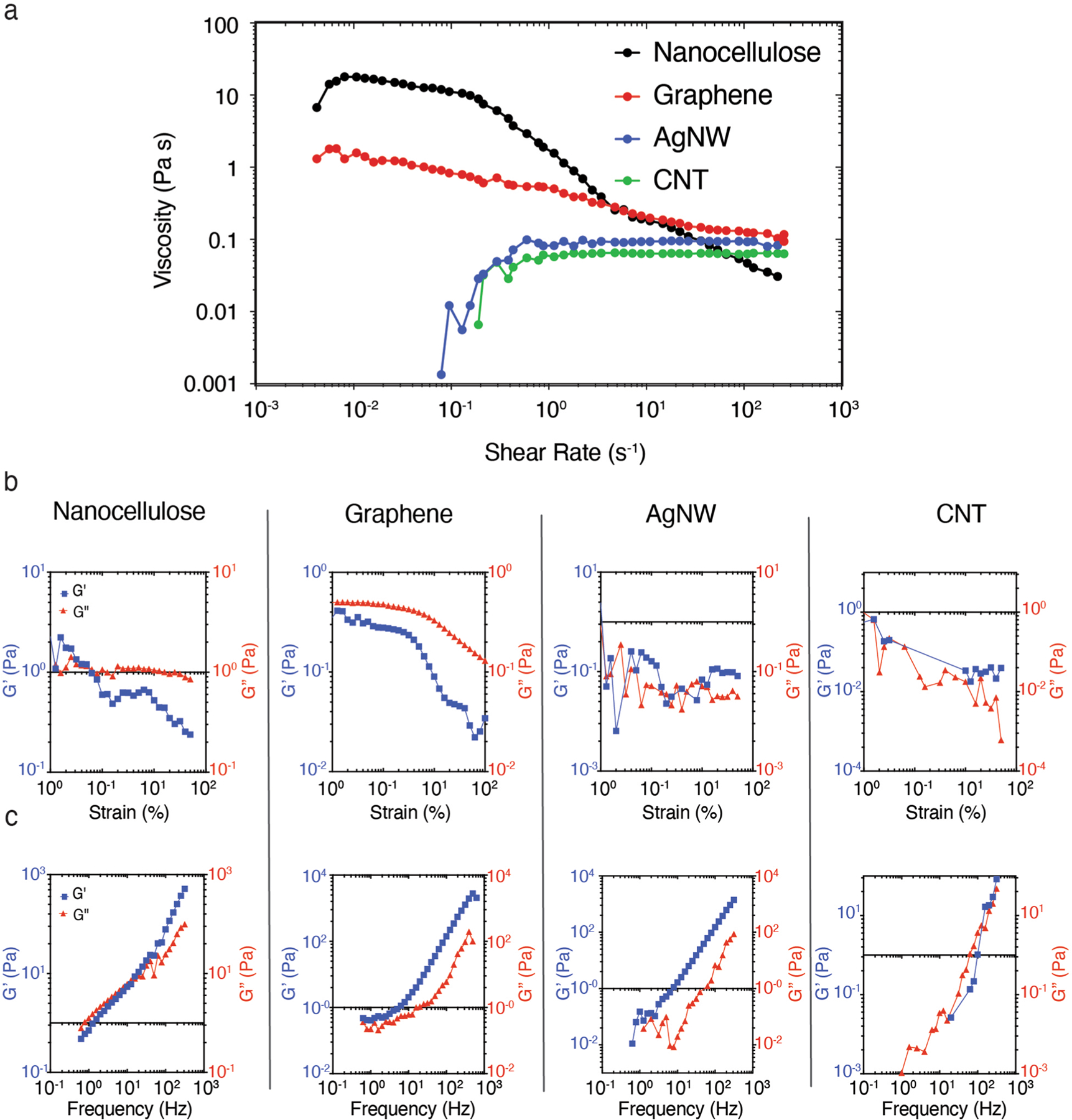
a, Dynamic Viscosities of all inks as a function of shear rates. b, Strain dependent storage (G’, blue line) and loss (G”, red) moduli, measured at a frequency of 1 Hz, for nanocellulose ink (first column), graphene ink (second column), silver nanowire ink (third column) and carbon nanotube ink (fourth column). c, Frequency dependent storage (G’, blue line) and loss (G”, red) moduli. it should be noted that the viscosities of the AgNW and the CNT inks are approaching the measurement limits of the rheometer.
Extended Data Fig. 2 |. Characterization of printed inks.
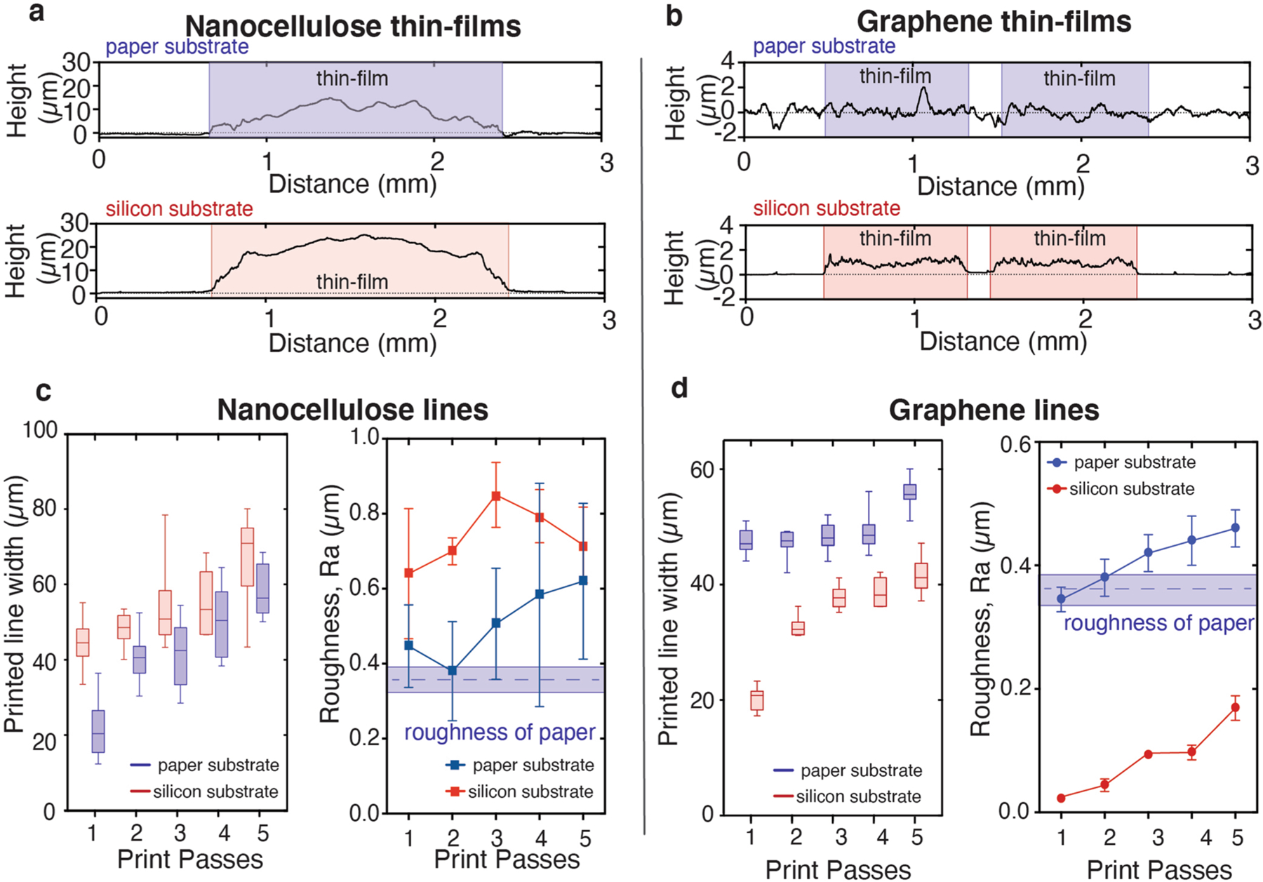
a, Heights of single pass nanocellulose thin-films printed onto a paper substrate (top) and silicon substrate (bottom). Boxed region represents printed thin-film area. The height of the CNC thin-film is most likely lower on the paper substrate due to impregnation of the nanocellulose film into the fibrous paper. b, Heights of graphene thin-films printed onto a paper substrate (top) and silicon substrate (bottom). Boxed region represents printed thin-film area. No graphene height can be observed on the paper substrate due to wicking of the ink into the paper substrate. c, printed line widths (left) for nanocellulose lines printed onto paper substrates (blue) and silicon substrates (red) as a function of print passes. Box represents lower and upper quartile range, line represents median, and whiskers represent lowest and highest value. Line widths represent 10 width measurements from 1 print. printed line roughness values (right) for nanocellulose lines. Datapoints represent average and standard deviation of 5 profilometry measurements taken from 1 print. d, Graphene line widths (left) and roughness values (right) for printed lines on paper substrates (blue) and silicon substrates (red).
Extended Data Fig. 3 |. Crystalline Nanocellulose dielectric characterization.
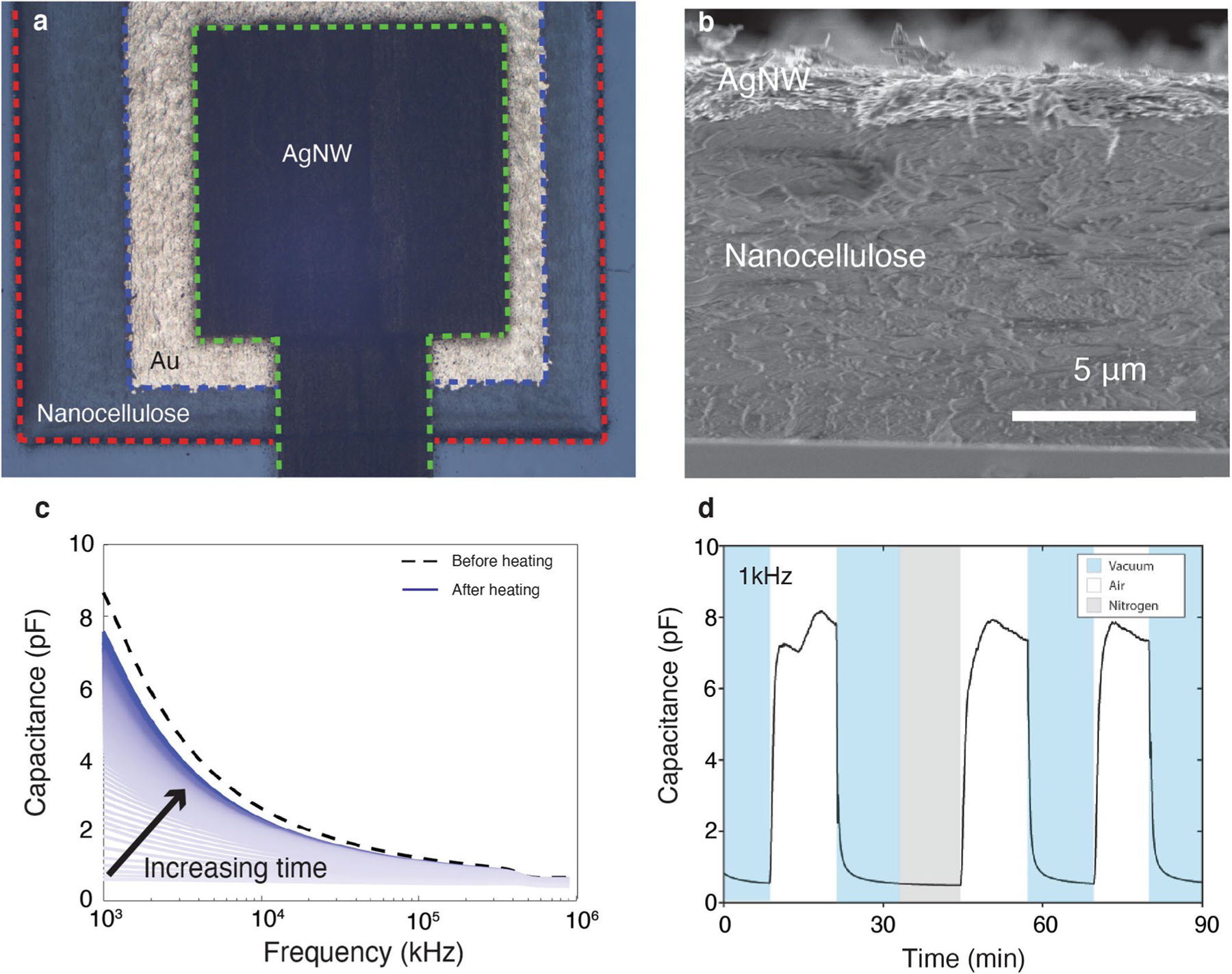
a, Top-view optical image and (b) SEM cross-sectional image of nanocellulose parallel plate capacitor. c, Capacitance as a function of frequency for nanocellulose capacitor before heating (dashed line) and after heating to 80 °C for 1 hour (solid blue lines) measured every 30 seconds for 30 minutes (light to dark blue), indicating strong frequency dependence of capacitance and a recoverable decay of low-frequency capacitance after heating. d, Capacitance response to atmosphere conditions in vacuum (blue), air (white), and nitrogen (grey). Both tests demonstrate hydration dependence on capacitance with a decrease in low-frequency capacitance after water evaporation due to heat and vacuum, respectively. The nitrogen atmosphere demonstrates that the capacitance decrease is caused by a hydration decrease as opposed to an environmental pressure change.
Extended Data Fig. 4 |. Crystalline nanocellulose capacitance-charge relationship.
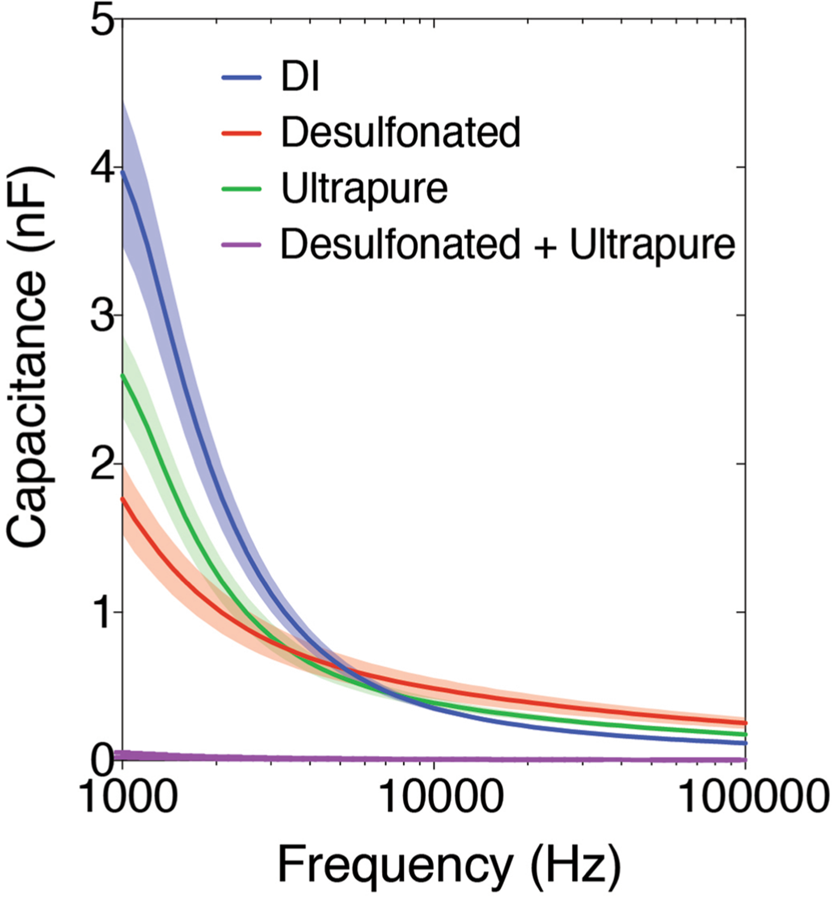
Nanocellulose capacitance as a function of frequency measured on parallel plate capacitors for nanocellulose dielectric films printed with 6% w/w crystalline nanocellulose in Di water (blue), 6% desulfonated crystalline nanocellulose in Di water (red), 6% crystalline nanocellulose in ultrapure water (green), and 6% desulfonated crystalline nanocellulose in ultrapure water (purple). This illustrates that the intrinsic ionic nature of the nanocellulose dielectric is derived from the dissolved salts in addition to the sulfonation from the hydrolysis of cellulose. Data represent average ± standard deviation of 4 devices.
Extended Data Fig. 5 |. Nanocellulose-based all-carbon TFT electrical characterization.
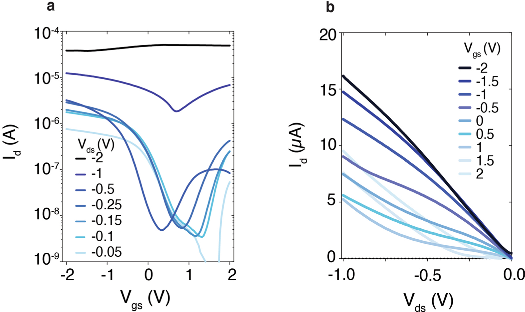
a, Subthreshold curves at varying drain-sourcevoltages (Vds) demonstrating the optimization of on/off-current ratio at a Vds of −0.5 V. b) Output curves at varying gate voltages. A clear shift in conduction pathway can be seen at increasingly positive Vgs where carriers are now tunneling through the Schottky barrier into the conduction band rather than the lower-barrier injection of carriers into the valence band at negative gate bias. The transistors were fabricated with a 0.15 mM salt concentration in crystalline nanocellulose and tested with a sweep frequency of 10 ms.
Extended Data Fig. 6 |. All-carbon TFT back-to-back cycling without added salt in nanocellulose dielectric.
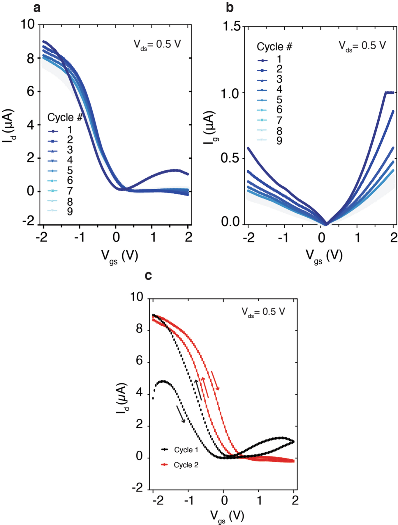
a, Transfer curves (drain current plotted on a linear scale against gate voltage) and (b) corresponding gate leakage currents demonstrating a 15% decrease in on-current and a 77% decrease in leakage current over 9 cycles, attributed to limitations in ion mobility and a time delay in the development of a double layer in the nanocellulose dielectric. c, Transfer curves for two back-to-back cycles showing a marked decrease in hysteresis between the (black) first and (red) second cycles and a significant (~2x) increase in on-current, attributed to the slow formation of the double layer charge that guides the decrease in gate leakage. Without the addition of salt, the transistor behavior is highly dependent on device history, both in terms of cycle duration (hold time) and in terms of cycle number. The transistor was fabricated without added salt and tested with a sweep rate of ~mV s−1.
Extended Data Fig. 7 |. Viscosity of crystalline nanocellulose ink with added mobile ions.
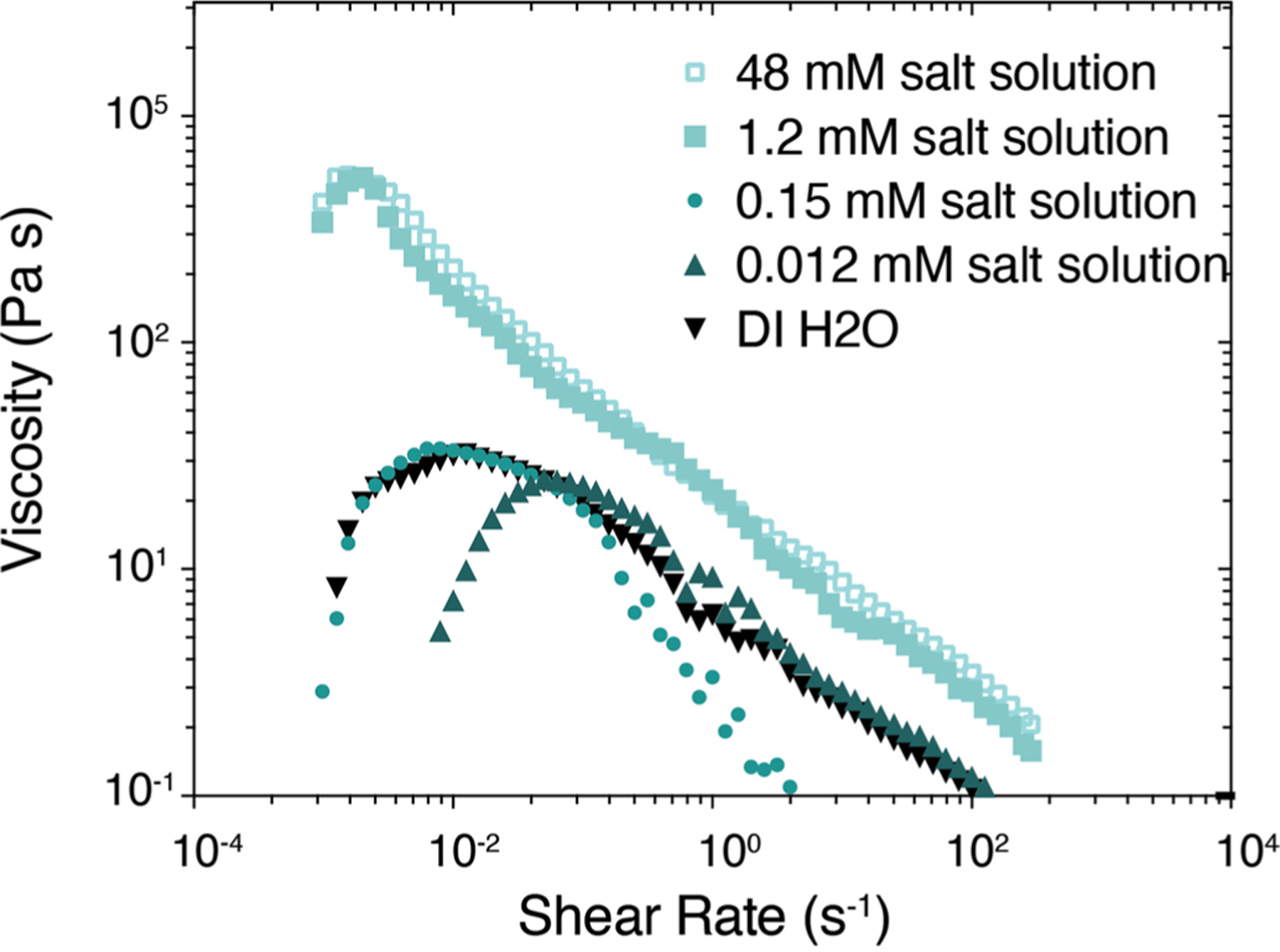
Dynamic viscosity of 6% crystalline nanocellulose solutions with increasing salt concentrations demonstrating the electroviscous effect.
Extended Data Fig. 8 |. lactate biosensing from fully printed all-carbon devices on paper.
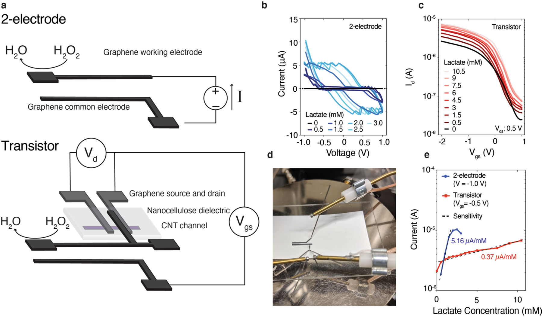
a, Schematic of (top) 2-electrode and (bottom) transistor-based, all-carbon lactate sensors. Electronic lactate concentration testing using (b) the 2-electrode sensor and (c) the transistor-based sensor. d, Transistor-based testing setup. e, Current dependence on lactate concentration showing a more pronounced current response to increases in lactate concentration with the 2-electrode device; however, a current maximum is reached at a concentration that is too small for medical relevance whereas the transistor-based device extends the sensing window by at least 5x, allowing for medically relevant lactate sensing. Lactate concentrations greater than 2 mM in human blood are indicative of septic shock. Furthermore, recent research indicates that mortality rates for patients presenting with elevated lactate concentrations was highly dependent on the duration of sepsis. Mortality sharply declined when lactate levels stabilized to a value of 2.2 mM as opposed to those that maintained a concentration of 3.3 mM after 4 hours. Hence, the 2-electrode sensor, which has a higher sensitivity than the transistor-based sensor (5.16 μA mM−1 vs 0.37 μA mM−1, respectively) has a sensing window that is too narrow for complete medical relevance. Working electrode area is 5 mm2 for all measurements).
Extended Data Fig. 9 |. Nanomaterial ink recycling yield.
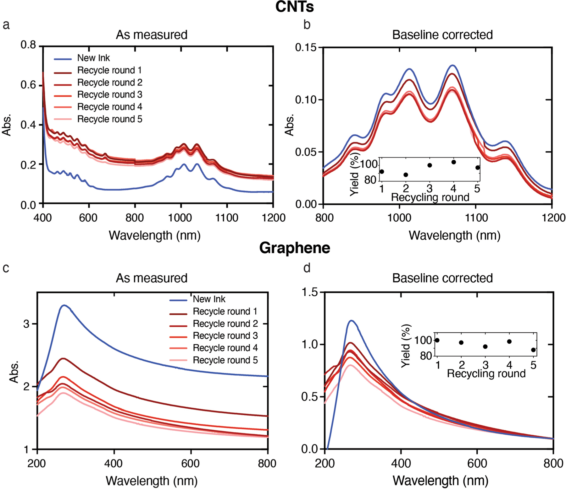
a, New CNT ink (blue) and 5x recycling iterations of CNT ink (red—dark→light; recycling cycles 1→5). The difference in baseline absorbance (away from the CNT peaks) between inks at ostensibly the same concentration may be due to some particulate matter left in the ink. b, To allow for CNT concentration measurement, the baselines were aligned and plotted and the area under the curve from a wavelength of 800–1200 nm was measured. The percent yield (insert) was measured by subtracting the integrands (that is recycling round 1: ). c, New (blue) and 5x recycling iterations of graphene ink (red—dark→light; recycling cycles 1→5). With the graphene ink the baseline absorbance (away from the graphene peak) is markedly higher for the new ink, potentially due to the added viscosifiers. b, baseline corrected graphene ink absorbance with recycling yield (insert). Graphene ink integration was measured from 200—800 nm.
Extended Data Fig. 10 |. CNT printing density.
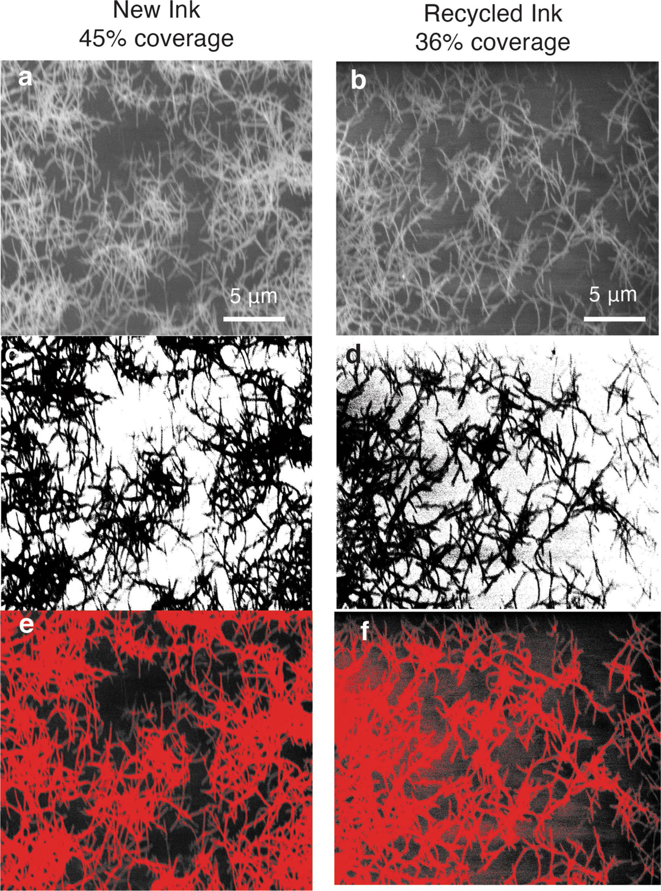
SEM images of CNT thin films printed on silicon using (a) pristine and (b) recycled CNT ink for purposes of determining printed density (45% and 36% coverage for new and recycled inks, respectively). c,d, For analysis, each image was set to binary using imageJ, and in addition, in e,f, the color threshold was modified to help guide the eye. The decrease in printed ink density may help explain the slightly lower on-current with the recycled CNT ink.
Supplementary Material
Acknowledgements
This work was performed in part at the Duke University Shared Materials Instrumentation Facility (SMIF), a member of the North Carolina Research Triangle Nanotechnology Network (RTNN), which is supported by the National Science Foundation (grant no. ECCS-1542015) as part of the National Nanotechnology Coordinated Infrastructure (NNCI). This work was supported by the Department of Defense Congressionally Directed Medical Research Program (CDMRP) under award no. W81XWH-17–2-0045 and by the National Institutes of Health (NIH) under award no. 1R01HL146849. G.B. and M.J.T. are grateful to the Air Force Office of Scientific Research for research support under award no. FA9550–18-1–0222.
Footnotes
Competing interests
The authors declare no competing interests.
Additional information
Extended data is available for this paper at https://doi.org/10.1038/s41928-021-00574-0.
Supplementary information The online version contains supplementary material available at https://doi.org/10.1038/s41928-021-00574-0.
Peer review information Nature Electronics thanks Seungjun Chung and Kamrul Hassan for their contribution to the peer review of this work.
Reprints and permissions information is available at www.nature.com/reprints.
Data availability
The data that support the plots within this paper and other findings of this study are available from the corresponding author upon reasonable request.
References
- 1.Jambeck J et al. Plastic waste inputs from land into the ocean. Science 347, 768–771 (2015). [DOI] [PubMed] [Google Scholar]
- 2.Hwang S-W et al. A physically transient form of silicon electronics. Science 337, 1640–1644 (2012). [DOI] [PMC free article] [PubMed] [Google Scholar]
- 3.Boutry CM et al. Biodegradable and flexible arterial-pulse sensor for the wireless monitoring of blood flow. Nat. Biomed. Eng 3, 47–57 (2019). [DOI] [PubMed] [Google Scholar]
- 4.Rüegg M, Blum R, Boero G & Brugger J Biodegradable frequency-selective magnesium radio-frequency microresonators for transient biomedical implants. Adv. Funct. Mater 29, 1903051 (2019). [Google Scholar]
- 5.Tan MJ et al. Biodegradable electronics: cornerstone for sustainable electronics and transient applications. J. Mater. Chem C 4, 5531–5558 (2016). [Google Scholar]
- 6.Teng L et al. Liquid metal-based transient circuits for flexible and recyclable electronics. Adv. Funct. Mater 29, 1808739 (2019). [Google Scholar]
- 7.Liu H, Li J & Tan R Flexible In2O3 nanowire transistors on paper substrates. IEEE J. Electron Devices Soc 5, 141–144 (2017). [Google Scholar]
- 8.Irimia-Vladu M ‘Green’ electronics: biodegradable and biocompatible materials and devices for sustainable future. Chem. Soc. Rev 43, 588–610 (2014). [DOI] [PubMed] [Google Scholar]
- 9.Li Y, Misra M & Gregori S Printing green nanomaterials for organic electronics. IEEE Trans. Compon. Packaging Manuf. Technol 8, 1307–1315 (2018). [Google Scholar]
- 10.Banerjee K et al. Prospects of carbon nanomaterials for next-generation green electronics In Proc. 10th IEEE Conference on Nanotechnology, NANO 2010 56–61 (IEEE, 2010); 10.1109/NANO.2010.5698053 [DOI] [Google Scholar]
- 11.Andrews JB et al. Fully printed and flexible carbon nanotube transistors for pressure sensing in automobile tires. IEEE Sens. J 18, 7875–7880 (2018). [Google Scholar]
- 12.Schroeder V, Savagatrup S, He M, Lin S & Swager TM Carbon nanotube chemical sensors. Chem. Rev 119, 599–663 (2019). [DOI] [PMC free article] [PubMed] [Google Scholar]
- 13.Jesadabundit W, Chaiyo S, Siangproh W & Chailapakul O Simple and cost-effective electrochemical approach for monitoring of vitamin K in green vegetables. ChemElectroChem 7, 155–162 (2020). [Google Scholar]
- 14.Gaspar D et al. Nanocrystalline cellulose applied simultaneously as the gate dielectric and the substrate in flexible field effect transistors. Nanotechnology 25, 094008 (2014). [DOI] [PubMed] [Google Scholar]
- 15.Petritz A et al. Cellulose as biodegradable high-k dielectric layer in organic complementary inverters. Appl. Phys. Lett 103, 153303 (2013). [Google Scholar]
- 16.Xia M, Cheng Z, Han J & Zhang S Extremely stretchable all-carbon-nanotube transistor on flexible and transparent substrates. Appl. Phys. Lett 105, 143504 (2014). [Google Scholar]
- 17.Zhang Z, Zhang M, Du C, Li L & Chang KC Improving performance of all-carbon-nanotube thin-film transistors by low temperature supercritical CO2 fluid activation. IEEE Electron Device Lett 40, 921–924 (2019). [Google Scholar]
- 18.Li B et al. All-carbon electronic devices fabricated by directly grown single-walled carbon nanotubes on reduced graphene oxide electrodes. Adv. Mater 22, 3058–3061 (2010). [DOI] [PubMed] [Google Scholar]
- 19.Abdelmalik AA, Fothergill JC & Dodd SJ Aging of Kraft paper insulation in natural ester dielectric fluid In Proc. 2013 IEEE International Conference on Solid Dielectrics (ICSD) 541–544 (IEEE, 2013); 10.1109/ICSD.2013.6619678 [DOI] [Google Scholar]
- 20.Hamedi MM et al. Highly conducting, strong nanocomposites based on nanocellulose-assisted aqueous dispersions of single-wall carbon nanotubes. ACS Nano 8, 2467–2476 (2014). [DOI] [PubMed] [Google Scholar]
- 21.Parate K et al. Aerosol-jet-printed graphene electrochemical histamine sensors for food safety monitoring. 2D Mater 7, 034002 (2020). [Google Scholar]
- 22.Jettable Fluid Formulation Guidelines (Fujifilm Dimatix, 2013). [Google Scholar]
- 23.McManus D et al. Water-based and biocompatible 2D crystal inks for all-inkjet-printed heterostructures. Nat. Nanotechnol 12, 343–350 (2017). [DOI] [PubMed] [Google Scholar]
- 24.McKerricher G, Perez JG & Shamim A Fully inkjet printed RF inductors and capacitors using polymer dielectric and silver conductive ink with through vias. IEEE Trans. Electron Devices 62, 1002–1009 (2015). [Google Scholar]
- 25.Pu J et al. Highly flexible MoS2 thin-film transistors with ion gel dielectrics. Nano Lett 12, 4013–4017 (2012). [DOI] [PubMed] [Google Scholar]
- 26.Cardenas JA et al. Impact of morphology on printed contact performance in carbon nanotube thin-film transistors. Adv. Funct. Mater 29, 1805727 (2019). [Google Scholar]
- 27.Higgins TM et al. Electrolyte‐gated n‐type transistors produced from aqueous inks of WS2 nanosheets. Adv. Funct. Mater 29, 1804387 (2018). [Google Scholar]
- 28.Chen L et al. Tailoring the yield and characteristics of wood cellulose nanocrystals (CNC) using concentrated acid hydrolysis. Cellulose 22, 1753–1762 (2015). [Google Scholar]
- 29.Zou Z et al. Rehealable, fully recyclable and malleable electronic skin enabled by dynamic covalent thermoset nanocomposite. Sci. Adv 4, eaaq0508 (2018). [DOI] [PMC free article] [PubMed] [Google Scholar]
- 30.Martins RFP et al. Recyclable, flexible, low-power oxide electronics. Adv. Funct. Mater 23, 2153–2161 (2013). [Google Scholar]
- 31.Williams NX et al. Silver nanowire inks for direct-write electronic tattoo applications. Nanoscale 11, 14294–14302 (2019). [DOI] [PMC free article] [PubMed] [Google Scholar]
- 32.Lu S et al. Uniform and stable aerosol jet printing of carbon nanotube thin-film transistors by ink temperature control. ACS Appl. Mater. Interfaces 12, 43083–43089 (2020). [DOI] [PMC free article] [PubMed] [Google Scholar]
- 33.Moberg T et al. Rheological properties of nanocellulose suspensions: effects of fibril/particle dimensions and surface characteristics. Cellulose 24, 2499–2510 (2017). [Google Scholar]
- 34.Phan-Xuan T et al. Aggregation behavior of aqueous cellulose nanocrystals: the effect of inorganic salts. Cellulose 23, 3653–3663 (2016). [Google Scholar]
- 35.Wu Q, Li X, Fu S, Li Q & Wang S Estimation of aspect ratio of cellulose nanocrystals by viscosity measurement: influence of surface charge density and NaCl concentration. Cellulose 24, 3255–3264 (2017). [Google Scholar]
Associated Data
This section collects any data citations, data availability statements, or supplementary materials included in this article.
Supplementary Materials
Data Availability Statement
The data that support the plots within this paper and other findings of this study are available from the corresponding author upon reasonable request.


