Abstract
Low dark current density plays a key role in determining the overall performance of perovskite photodetectors (PPDs). To achieve this goal, a hole transport layer (HTL) on the ITO side and a hole blocking layer (HBL) on the metal electrode side are commonly introduced in PPDs. Unlike traditional approaches, we realized a high-performance solution-processed broadband PPD using metal oxide (MO) nanoparticles (NPs) as the HBL on the ITO electrode and PC61BM as another HBL on the metal electrode side to reduce the device dark current. The PPDs based on TiO2 and SnO2 NP-modified layers show similar device performances at −0.5 V: a greater than 105 on/off ratio; over 100 dB linear dynamic range (LDR) under different visible light illumination; around 0.2 A W−1 responsivity (R); greater than 1012 jones detectivity (D*); and ∼20 μs rise time of the device. The MO NP interfacial layer can significantly suppress charge injection in the dark, while the accumulated photogenerated charges at the interface between the MO layer and the perovskite layer introduce band bending, leading to dramatically increased current under illumination. Therefore, the dark current density of the devices is significantly reduced and the optical gain is drastically enhanced. However, after UV illumination, the dark current of the TiO2 device dramatically increases while the dark current of the SnO2 device can stay the same as before since the UV illumination-induced conductivity and barrier height changes in the TiO2 layer cannot recover after removing the UV irradiation. These results indicate that the TiO2 NP layer is suitable for making a vis-NIR photodetector, while the SnO2 NP layer is a good candidate for UV-vis-NIR photodetectors. The facile solution-processed high-performance perovskite photodetector using MO NP-modified ITO is highly compatible with low cost, flexible, and large-area electronics.
PPDs based on TiO2 and SnO2 NP layers show similar significantly low dark current density. Due to the UV induced conductivity and barrier height changes in the TiO2 device after UV illumination the dark current of the device increases, while the SnO2 device remains the same.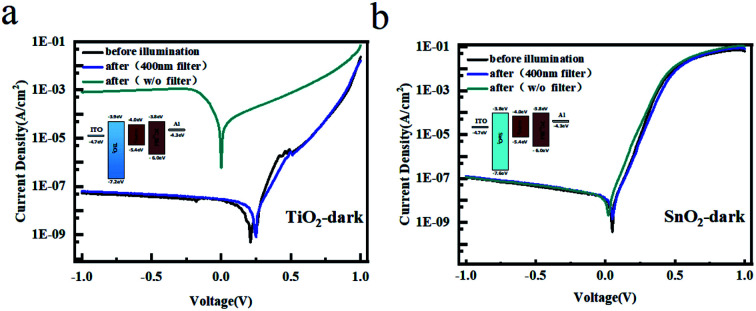
Introduction
Ever since solid organic–inorganic hybrid perovskites have been applied in solar cells, their power conversion efficiency (PCE) has rapidly risen from 3.8% 1 to over 25%.2 In addition to the significant progress seen in solar cells, perovskite materials have made a series of breakthroughs in light-emitting diodes (LEDs),3–5 amplified spontaneous emission (ASE) or lasers6,7 and photodetectors (PDs).8,9 Compared with traditional photodetectors based on Si,10 GaN,11,12 and GaAs,13,14 perovskite-based photodetectors have attracted much attention due to their unique advantages of low temperature solution process, tunable bandgap, high quantum efficiency, broad wavelength response, and large area application. However, the mass surface defects and grain boundaries result in solution-processed perovskite PDs usually suffering from a high dark current due to the trapped charge carrier-induced leakage current or enhanced charge injection under reverse bias.15 The dark current (Jd) plays a crucial role in determining the overall performance of PDs, impacting the signal-to-noise ratio (SNR), detectivity (D*), and linear dynamic range (LDR). Therefore, in common PPDs, a thin phenyl-C61-butyric acid methyl ester (PC61BM) film is usually deposited on top of the perovskites to passivate the defects.16 For superior device performance, various hole-blocking layers (HBL) have been added between the perovskite layer and the metal electrode to suppress the leakage current. Yang et al. introduced PEDOT as a hole transport layer (HTL) and poly[(9,9-bis(30-(N,N-dimethylamino)propyl)-2,7-fluorene)-alt-2,7-(9,9-dioctylfluorene)] (PFN) or 2,9-dimethyl-4,7-diphenyl-1,10-phenanthroline (BCP) as HBL to achieve a high on/off ratio of 105;17 Meredith et al. applied PEDOT and C60 on top of the ITO layer and PC61BM layer, respectively, to achieve low noise;18 Huang et al. coated the C60/BCP bilayer between PC61BM and Al to realize a low noise perovskite photodetector;19 Huang et al. used poly[bis(4-phenyl)(2,4,6-trimethylphenyl)amine] (PTAA) as HTL and IEICO/C60/BCP trilayer on top of the perovskite layer to demonstrate a highly sensitive photodetector;20 Yu et al. used 4,4′-cyclohexylidenebis[N,N-bis(p-tolyl) aniline] (TAPC) as HTL and introduced the PBDB/IHIC bulk heterojunction between the perovskite and PCBM to reduce the undesired high dark current;21 Chen et al. proposed a self-assembled polar monolayer (SAPM) as HTL and used PC61BM/PEI as HBL to achieve high performance; Alshehri et al.,22 Caironi et al.,23 Oh et al.,24 and Ruan et al.25 have demonstrated a series of high-performance perovskite photodetectors by introducing PDPP3T:PC61BM, PC61BM/AZO, PC61BM/TiOx, and PC61BM/PCBM:F4-TCNQ/BCP as the hole-blocking layer in the PEDOT-modified ITO-based perovskite photodetectors, respectively. The abovementioned works show that a typical high-performance PPD typically needs HTL on the ITO side and HBL on the metal electrode side. In these devices, PEDOT is usually used as HTL and the mixed layer or multi-layer containing fullerene is used as HBL. The poly(triaryl amine) (PTAA)-modified atomic layer deposition (ALD) ZnO film has also been explored to make high-performance perovskite photodetectors with a configuration of ITO/ZnO/PTAA/perovskite/PC61BM/Ag.26 It should be mentioned that, unlike TiO2 or SnO2, when the annealing temperature is greater than 100 °C, ZnO can react with perovskite and affect the film formation and stability of the perovskite.27–29 Therefore, in order to get a better perovskite film on ZnO, it is usually necessary to add a modified layer on ZnO or anneal ZnO at high temperature in advance to form a more compact ZnO film. Different from previous studies, we propose and demonstrate a high-performance PPD using MO NP HBL on the ITO side and PCBM HBL on the Al side. Either in-house synthesized TiO2 NPs30 or commercial SnO2 31 were coated on ITO, as in our previously reported method, and both resulting PPDs show comparably low Jd of ∼40 nA cm−2 at −0.5 V, leading to greater than 105 SNR, more than 1012 jones D*, and over 100 dB LDR under different light illuminations. Moreover, the comparison of UV illumination effects on the dark current of the TiO2 and SnO2 devices reveals that the former is suitable for vis-NIR photodetector application, while the latter is good for UV-vis-NIR photodetector application. This novel device structure with the single hole blocking layer on both ITO and Al sides not only significantly reduces the dark current of the device, but also greatly simplifies the device fabrication process, paving a new way for high-performance perovskite photodetector fabrications.
Results and discussion
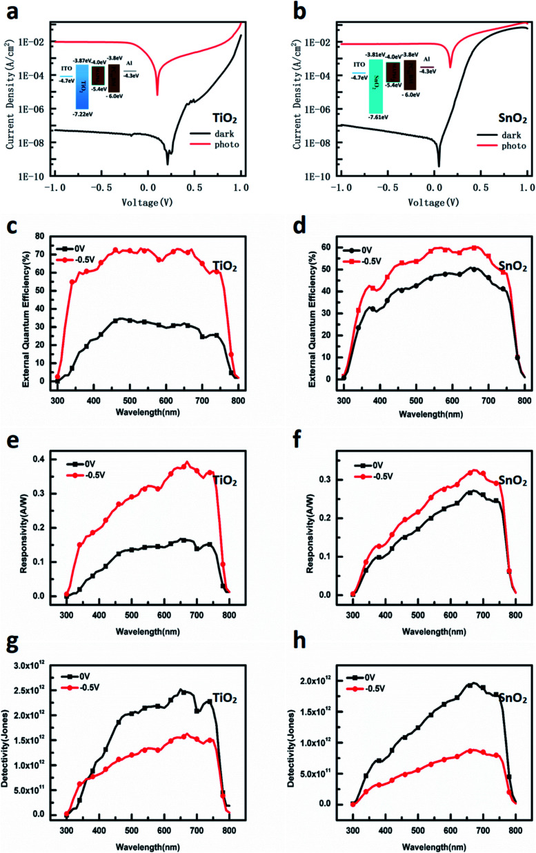
The energy diagrams of the devices are shown in the insets of Fig. 1a and b, respectively. The thin TiO2 or SnO2 NP layer was employed on top of the ITO as HBL. The TiO2 nanoparticles and SnO2 nanoparticles have similar conduction band minimum (CBM) and valence band maximum (VBM), and they are −3.9 eV/−3.8 eV and −7.2 eV/−7.6 eV, respectively. The MAPbI3 layer was used as a light-absorber and the PC61BM film was spin-coated on the top of the perovskite layer as the top HBL. The J–V curves of the TiO2 and SnO2 devices were measured under the bias from 1 V to −1 V, as shown in Fig. 1a and b. In the dark, the low current densities are 3.81 × 10⁻⁸ A cm−2 for the TiO2 device and 4.43 × 10⁻⁸ A cm−2 for the SnO2 device at −0.5 V, respectively, indicating that the charge injection is significantly suppressed at both cathode and anode interfaces. The current rectification implies that the electron injection from the Al electrode through the whole device is obviously easier than that from the ITO electrode because of the higher barrier height between ITO and the TiO2 or SnO2 layer. Meanwhile, under standard AM 1.5 G sunlight illumination, the current density of both devices increase to 10−3 A cm−2 (9.03 × 10⁻³ A cm−2 for the TiO2 device and 7.39 10−3 A cm−2 for the SnO2 device at −0.5 V). Therefore, over 105 on/off ratio (2.36 × 10⁵ at −0.5 V for the TiO2 device, 1.67 × 10⁵ at −0.5 V) can be achieved, comparable to previously reported results.17,20,21,23,24,32
Fig. 1. The J–V characteristics of the devices in the dark or under illumination, and the schematic energy level diagram of the devices: (a) the device based on TiO2 nanoparticles, (b) the device based on SnO2 nanoparticles; the photoresponse of the devices: (c, e and g) the EQE, R, and D* of the TiO2 device, respectively; (d, f and h) the EQE, R, and D* of the SnO2 device, respectively.
The external quantum efficiency (EQE) is an important parameter that characterizes the ratio between the number of photo-induced charge carriers collected by the external circuit and the number of incoming photons. The EQE of the devices was measured at 0 V and −0.5 V, and the results are shown in Fig. 1c, d. The scanning wavelength is from 300 to 850 nm, and the maximum EQE values of the TiO2 device and the SnO2 device at 0 V are 33% and 51%, respectively. At −0.5 V, the maximum EQE values for the TiO2 device and the SnO2 device increase to 73.4% at 530 nm and 60.1% at 670 nm, respectively. Responsivity (R) is the ratio of output current to input optical power, which can be calculated from EQE using the following eqn (1):
| R = EQEq/hυ | 1 |
where hυ is the energy of the incident photon and q is the elementary charge of the electron. The ability to detect the optical signals from the noise is usually measured by detectivity, which can be calculated by the eqn (2):
 |
2 |
where Jdark is the dark current density. The corresponding R and D* of the TiO2 device and the SnO2 device are shown in Fig. 1e and f. The maximum R is around 0.32 A W−1 (−0.5 V) for the TiO2 device, and it is 0.26 A W−1 for the SnO2 device (−0.5 V). The D* of the TiO2 device (Fig. 1g) reaches 2.17 × 10¹² (0 V, 550 nm) while that of the SnO2 device (Fig. 1h) is 1.52 × 10¹² (0 V, 550 nm). It is worth noting that the detectivity decreases when the bias increases from 0 V to −0.5 V, attributed to the increase of the dark current.
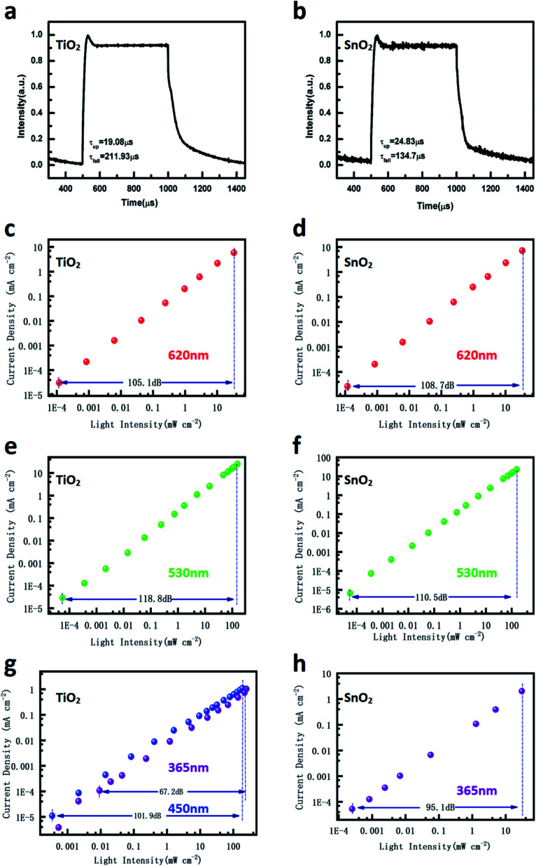
Response time is another critical parameter for the practical application of the photodetector. It includes the rise time and fall time: the former is defined as the time required for the current value to increase from 10% to 90% of the maximum value, and the latter is the current value falling from 90% to 10% of the peak value. Rise time reflects the process of generation, diversion, transportation, and collection of the photo-induced carriers, while fall time is dependent on the release of the trapped carriers by defects when the light source is removed. The response times of the two devices were measured under the illumination of 530 nm light at −0.5 V, and the results are shown in Fig. 2a and b. The rise time for the TiO2 and SnO2 devices are 19.08 μs and 24.83 μs, respectively. The fall time of the SnO2 device is 134.7 μs and the TiO2 device is 211.93 μs, indicating that the trapped charges in the TiO2 NP layer need more release time than those in the SnO2 NP layer. From the practical perspectives, LDR is very crucial for the photodetector. LDR is defined as the range over which the photocurrent is linear with light intensity. Beyond this range, the relationship between the light signal and electrical signal is not linear anymore and the light signal cannot be calculated precisely. The devices were tested under the illuminations of 530 nm and 620 nm LEDs, respectively, and the results are shown in Fig. 2c–f. Both devices show a large linear range under different incident light intensities (power density ranges from 10−1 to 10−7 W cm−2), leading to a LDR of over 100 dB. However, when the devices were tested under the illumination of UV light (Fig. 2g and h), the LDR of TiO2 is significantly dropped to 65 dB while the SnO2 still has 95 dB value. When using 450 nm light, the LDR of the TiO2 device changes back to 100 dB, implying the significantly different sensitivities between the TiO2 and SnO2 NP layer to UV light.
Fig. 2. Response time of (a) the TiO2 device; (b) the SnO2 device; LDRs of the TiO2 and SnO2 devices measured at −0.5 V under various wavelength illuminations (c–h).
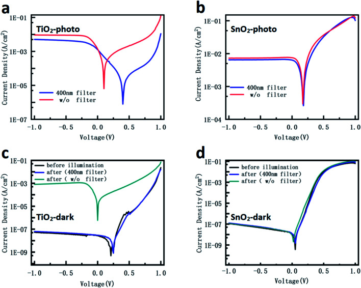
The wavelength (with or without UV)-dependent J–V curves were measured and the results are shown in Fig. 3. As Fig. 3a and b show, compared with the sunlight illumination, when a 400 nm filter is used, the photocurrents under bias for both devices are slightly reduced. In contrast, the open voltage of the SnO2 device does not show obvious changes under different wavelength illuminations, while the open voltage of the TiO2 device increases by about 0.3 V compared with the added UV illumination. Considering the same structure and measurement condition, the result is attributed to the different UV sensitivities to the TiO2 NP layer compared with the SnO2 NP layer. The dark currents of the two devices were measured after different light exposures for 1 min, as shown in Fig. 3c and d. When the TiO2 device was exposed under illumination without UV wavelength, the device dark current was retested and the valve is almost the same as the one before illumination. However, after illumination with the full wavelength, the dark current increases to a high level, which illustrates that the device is highly conductive. The SnO2 device shows consistently low dark current before and after illumination with or without UV wavelength. These behaviors indicate that the short-term UV illumination induces longtime effects in the TiO2 device, but not in the SnO2 device. It has been widely reported that TiO2 has photocatalysis property under UV light and SnO2 is not sensitive to UV light.33,34 Therefore, the results suggest that the UV illumination-induced carriers may store in the TiO2 NP layer, which would influence its conductivity and the energy level, resulting in a high dark current when removing the illumination and the different output property with or without UV light.
Fig. 3. The wavelength-dependent J–V curves of the TiO2 device: (a) under illumination, (c) in the dark; and the SnO2 device: (b) under illumination, (d) in the dark.
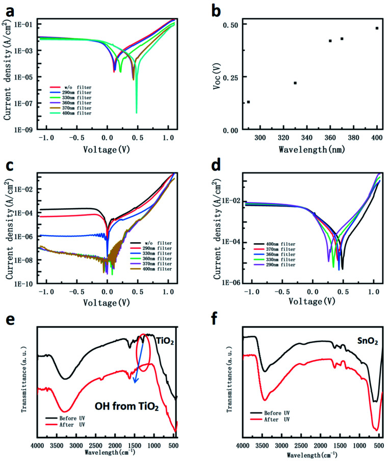
As shown in Fig. 4a and b, different wavelength filters are used to distinguish the influence of various wavelength lights for the TiO2 device. The Voc gradually decreases from 0.48 V to 0.13 V when the filters from 370 nm to 330 nm are used. Compared with the Voc of the device under full wavelength illumination, the value used 290 nm filter does not obviously change. This result suggests that with the shorter wavelength light absorbed by the TiO2 NPs, there is a larger Fermi energy level change in the TiO2 NP layer. Fig. 4c and d show the dark currents and the light currents under illuminations with a 400 nm filter of the devices after different light exposure conditions, as shown in Fig. 4a. Similar to the above observations, shortening the illumination wavelength can significantly increase the dark current of the device. Moreover, the photocurrent (Fig. 4d) shows that the UV illumination-induced Voc change shown in Fig. 4a cannot recover to the maximum value, indicating that the energy level change remained.
Fig. 4. (a and b) The J–V curves and specific Voc value of the TiO2 device under different light conditions; (c) the dark currents of the devices after the different light conditions shown in (a); (d) light currents under illumination with a 400 nm filter of the devices after the different exposure conditions shown in (a); the Fourier transform infrared spectroscopy of (e) TiO2 and (f) SnO2 nanoparticles: red line (black line) is the FTIR spectroscopy of the film after (before) UV illumination for 5 min.
It is well known that the UV absorption of the TiO2 nanoparticle is highly effective.35 Through spectroelectrochemical methods, Donald Fitzmaurice's group has concluded that the surface states of anatase TiO2 are located at about 0.5 eV below the conduction band.36,37 Other works have also shown the existence of a trap state below the conduction band.38–40 Many groups have reported that the UV exposure can positively shift the conduction band of the TiO2 NP film.41–44 It has been demonstrated that the filling of surface states or UV exposure makes the TiO2 NP film more conductive,39,45–47 and reduces the barrier height between ITO and the TiO2 nanoparticle.48–50 Therefore, the variation of the output characteristics and dark current of the TiO2 device after the illumination is most likely caused by the UV exposure/filling surface state-induced change of the energy band and conductivity of the TiO2 NP film.
Fig. 4e and f show the FTIR spectroscopy of the TiO2 and SnO2 NP films before and after 5 min UV exposure, respectively. The vibration absorption peaks between 3000 and 3800 cm−1 and 1200–1800 cm−1 correspond to the hydroxyl in the H2O molecule and hydroxyl on the TiO2 surface, respectively.51 The results show that the peak attributed to the hydroxyl on the TiO2 surface disappears in the TiO2 NP film after UV illumination for 5 min. However, there is no obvious peak change in the SnO2 NP film, indicating that the UV light does not make an obvious change in the SnO2 NP film. The Ti–OH bond plays an important role in the surface states of the TiO2 nanoparticle.52 The oxygen molecule absorbed by hydroxyl and oxygen vacancies are considered as defects, which can trap free electrons from the conduction band of the TiO2 nanoparticle, and the conductivity of the metal oxide film thus decreases.52–54 The decomposition of the hydroxyl group reflects the reduction of the surface state, which has been reported in previous works.55,56 In addition, under UV exposure, the oxygen vacancy-induced surface defects ubiquitous in the metal oxide would trap electrons, leading to the band upshift. Therefore, the hydroxyl on the surface states or oxygen vacancies could influence both energy band and conductivity of TiO2.57–59 After UV treatment, the accumulation of electrons on the surface states or the reduction of defect states enhance the conductivity of TiO2 since the release of charge become less localized.60 In addition, the XPS measurements were conducted to evaluate the stability of the metal oxidation states before and after exposure to UV. The results (not shown here) show that the peak positions of the metal in both TiO2 and SnO2 films do not change significantly. This observation is consistent with the previous report that demonstrated that the oxidation state of titanium does not change significantly before and after UV.61
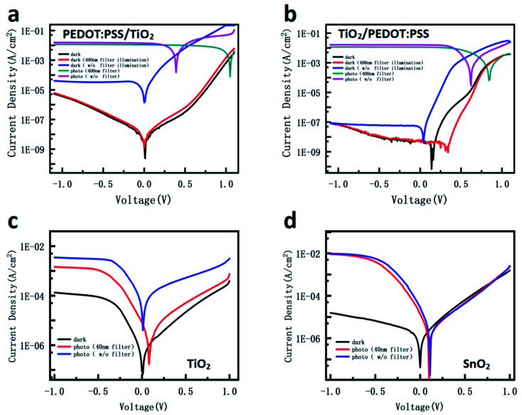
In addition, because the interface between TiO2 and perovskite would influence the dissociation of carriers and the injection of electrons,62 the interface effect on the dark current of the device needs to be clarified. PEDOT:PSS as a common hole transportation material was inserted between ITO/TiO2 or TiO2/perovskite to make various devices. Fig. 5a and b show the dark currents and photocurrents of the ITO/PEDOT:PSS/TiO2/perovskite device and the ITO/TiO2/PEDOT:PSS/perovskite device. The former has an obviously higher dark current compared with the latter, implying that the interface between ITO and TiO2 is another key to keep the low dark current. After the illumination without UV, both device dark currents remain the same as before. However, after the illumination with UV, the dark current of the ITO/TiO2/PEDOT:PSS device slightly increased, while that for the ITO/PEDOT:PSS/TiO2 device significantly increased in comparison with the dark current before illumination. The smaller dark current increase of the former device compared with the latter one is due to the insertion of PEDOT:PSS between TiO2 and perovskite. The most plausible reason is that the filling of the TiO2 trap states in the former is only contributed by the photo-generated charges in TiO2. Meanwhile, in the latter, it is contributed not only by photogenerated charges in TiO2, but also by the transferred photogenerated charges from perovskite since there is no interfacial layer between TiO2 and perovskite. Greater filling of the surface defects leads to a bigger change of energy band and conductivity of TiO2, resulting in a higher dark current. In addition, the function of the difference between the two electrodes was investigated. When the ITO electrode is changed to a transparent Al film, both SnO2 and TiO2 devices show a large increase of the dark current, as shown in Fig. 5c and d. The results further confirm that the Schottky barrier between the electrode and oxide metal contributed to the inhibition of charge injection.
Fig. 5. (a and b) J–V curves of the ITO/PEDOT:PSS/TiO2/perovskite device and the ITO/TiO2/PEDOT:PSS/perovskite device. (c and d) J–V curves for both Al electrode devices: TiO2 device and SnO2 device.
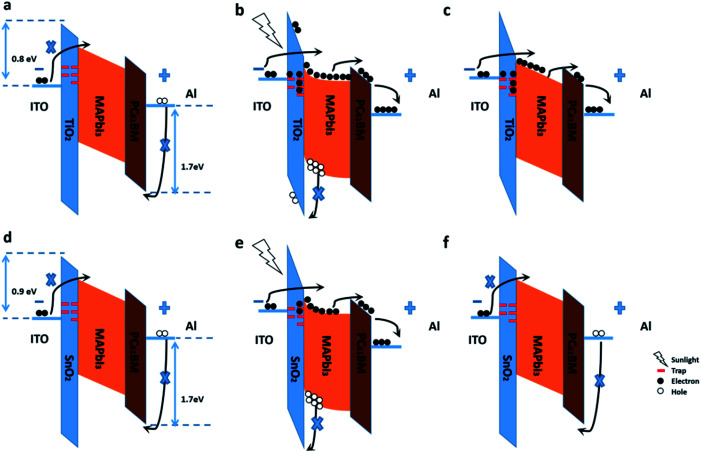
Finally, the mechanism is proposed as shown in Fig. 6. Under dark condition, the hole injection from the Al electrode and the electron injection from the ITO electrode are both significantly suppressed due to the high charge barriers (1.7 eV between Al and the valence band of PC61BM, 0.8/0.9 eV between ITO and the conduction band of TiO2/SnO2). Besides, the surface states of the TiO2/SnO2 NPs make the device remain at low conductivity, resulting in a low device dark current. Under illumination, free charge carriers are generated in the perovskite layer, the photo-generated holes are accumulated at the interface between the metal oxide and perovskite due to the interfacial barrier. The accumulated holes at the interface result in band bending, and the conductivity of the metal oxide NP film increases when the trap states of the nanoparticles are occupied by the photogenerated charge carriers. Therefore, a large number of electrons can be injected into the device from the ITO electrode, leading to a significantly larger photocurrent. In addition, unlike SnO2 NPs, the decrease in the hydroxyl release-induced trap state density and the trapped photogenerated carriers in the TiO2 NPs result in a long-term energy band shift and conductivity increase after UV illumination. Therefore, the dark current of the TiO2 device significantly increases, while the SnO2 is still as low as the one before illumination.
Fig. 6. The working principle schematics: the energy diagram of the TiO2 device: (a) in the dark, (b) under illumination, (c) in the dark after illumination; and the energy diagram of the SnO2: (d) in the dark, (e) under illumination, (f) in the dark after illumination.
Conclusions
In this work, we demonstrate a high-performance PPD using metal oxide nanoparticles as the hole-blocking layer on top of ITO and PC61BM as the hole-blocking layer under the Al electrode. The resulting significantly low dark current leads to a high on/off ratio and good performances for both TiO2 and SnO2 devices. After UV illumination, the dark current of the TiO2 device dramatically increases, while the dark current of the SnO2 device remains the same as before. Therefore, the TiO2 device is suitable for vis-NIR photodetector applications, while the SnO2 device is good for UV-vis-NIR photodetector applications. This novel device structure paves a new way for high-performance perovskite photodetector fabrications.
Experimental section
Materials
TiCl3 (15–20% basis in HCl) and absolute ethanol were purchased from Aladdin. The PbI2 (99.99%), MAI, HPLC water, N-dimethylformamide (DMF, 99.8%), and SnO2 colloid precursor (15% in H2O colloidal dispersion) were purchased from Alfa Aesar. PC61BM (99.5%) was purchased from Nano-C company.
Device fabrication
The ITO-coated glass substrates were pre-cleaned with deionized water and then ethanol in an ultrasonic bath for 30 minutes each time. Titanium trichloride was used as the titanium source to synthesize anatase TiO2 nanoparticles. The mixture of 60 mL ethanol, 2 mL TiCl3 and 1 mL HCl (6 M) was sealed to control the speed of the hydrolysis reaction, and were heated in the oven at 75 °C for around 8–10 h. The deposition was washed by anhydrous ethanol three times and the final products were dispersed into water for device fabrication. PbI2 and MAI were dissolved in DMF as a common mole ratio 1.05 : 1 (the excess PbI2 was used for defect passivation and enhancing crystallization),63,64 with a concentration of 1.25 M and then stirred at 70 °C overnight. 20 mg PC61BM was dissolved in 1 mL chlorobenzene for over 8 h. The ultrasonic treatment of the solution was conducted before the device was fabricated.
The clean indium tin oxide (ITO)-coated glass substrates were treated in UV–ozone for 15 min before deposition of the SnO2 or TiO2 layer. The TiO2 solution (20 mg mL−1) was spin-coated at 2000 rpm for 50 s and the formed film was annealed at 130 °C for 10 minutes. The SnO2 solution (around 200 mg mL−1) was spin-coated at 7000 rpm for 40 s, and no further treatment was needed when the film was formed. The perovskite solution was deposited onto the prepared TiO2 or SnO2 film with a spin-coating speed of 2500 rpm for 10 s. During the spin coating process, 150 mL anti-solvent (chlorobenzene) was poured onto the spinning substrate to accelerate crystallization. The spin coating speed increased to 5000 rpm for 30 s. The formed perovskite films were heated at 100 °C for 10 minutes, resulting in the completion of crystallization. Furthermore, PC61BM (20 mg mL−1, dissolved in chlorobenzene) was spin-coated on the active layer at 1000 rpm for 30 s. Finally, a 100 nm thick aluminum film was deposited as the top electrode by thermal evaporation. In addition, a PEDOT:PSS layer can be fabricated by spin-coating a 60 μL precursor on the ITO substrate at 3000 rpm for 40 s and annealed at 140 °C for 10 min. Each device has an effective area of 4.5 mm2 (3 × 1.5 mm).
Characterization
The current density versus voltage (J–V) characteristic was measured with a Keithley 2450 instrument in a glovebox filled with N2. An Air Mass 1.5 Global (AM 1.5 G) solar simulator was used as the sunlight source with an irradiation intensity of 100 mW cm−2. The external quantum efficiency (EQE) was measured by a Zolix Solar Cell Scan 100 in the air. Different wavelength filters were used in front of the light outlet to cut off the short wavelength components to remove unwanted radiation. The Fourier transform infrared (FTIR) spectrum was measured with a Thermo Scientific Nicolet 6700 and the SnO2 or TiO2 solution was spin-coated onto the KBr substrate. For the transit photocurrent measurement, a square pulse optical excitation of 1 ms using a 530 nm LED driven by a WF 1946B multifunction synthesizer (NF Corporation) was used. In addition, an IT6133B DC power supply was used to provide different voltages and a NOVA II optical power meter was used to measure the light intensity.
Conflicts of interest
The authors declare no conflict of interest.
Supplementary Material
Acknowledgments
The authors acknowledge the financial support of the National Natural Science Foundation of China (No. 61975010, 62075009, 61875009, 61735004).
References
- Kojima A. Teshima K. Shirai Y. Miyasaka T. J. Am. Chem. Soc. 2009;131:6050–6051. doi: 10.1021/ja809598r. [DOI] [PubMed] [Google Scholar]
- Yoo J. J. Seo G. Chua M. R. Park T. G. Lu Y. Rotermund F. Kim Y. K. Moon C. S. Jeon N. J. Correa-Baena J. P. Bulovic V. Shin S. S. Bawendi M. G. Seo J. Nature. 2021;590:587–593. doi: 10.1038/s41586-021-03285-w. [DOI] [PubMed] [Google Scholar]
- Stranks S. D. Snaith H. J. Nat. Nanotechnol. 2015;10:391–402. doi: 10.1038/nnano.2015.90. [DOI] [PubMed] [Google Scholar]
- Tan Z. K. Moghaddam R. S. Lai M. L. Docampo P. Higler R. Deschler F. Price M. Sadhanala A. Pazos L. M. Credgington D. Hanusch F. Bein T. Snaith H. J. Friend R. H. Nat. Nanotechnol. 2014;9:687–692. doi: 10.1038/nnano.2014.149. [DOI] [PubMed] [Google Scholar]
- Cho H. Jeong S. H. Park M. H. Kim Y. H. Wolf C. Lee C. L. Heo J. H. Sadhanala A. Myoung N. Yoo S. Im S. H. Friend R. H. Lee T. W. Science. 2015;350:1222–1225. doi: 10.1126/science.aad1818. [DOI] [PubMed] [Google Scholar]
- Cho C. Palatnik A. Sudzius M. Grodofzig R. Nehm F. Leo K. ACS Appl. Mater. Interfaces. 2020;12:35242–35249. doi: 10.1021/acsami.0c08870. [DOI] [PubMed] [Google Scholar]
- Sutherland B. R. Sargent E. H. Nat. Photonics. 2016;10:295–302. doi: 10.1038/nphoton.2016.62. [DOI] [Google Scholar]
- Wangyang P. Gong C. Rao G. Hu K. Wang X. Yan C. Dai L. Wu C. Xiong J. Adv. Opt. Mater. 2018;6:1701302. doi: 10.1002/adom.201701302. [DOI] [Google Scholar]
- Mei F. Sun D. Mei S. Feng J. Zhou Y. Xu J. Xiao X. Adv. Phys.: X. 2019;4:1592709. [Google Scholar]
- Gruber G. Moses W. Derenzo S. Wang N. Beuville E. Ho H. Trans. Nucl. Sci. 1998;45:1063–1068. [Google Scholar]
- Kung P. Zhang X. Walker D. Saxler A. Piotrowski J. Rogalski A. Razeghi M. Appl. Phys. Lett. 1995;67:3792–3794. doi: 10.1063/1.115385. [DOI] [Google Scholar]
- Binet F. Duboz J. Rosencher E. Scholz F. Härle V. Appl. Phys. Lett. 1996;69:1202–1204. doi: 10.1063/1.117411. [DOI] [PubMed] [Google Scholar]
- Ting D. Z. Soibel A. Khoshakhlagh A. Rafol S. B. Keo S. A. Höglund L. Fisher A. M. Luong E. M. Gunapala S. D. Appl. Phys. Lett. 2018;113:021101. doi: 10.1063/1.5033338. [DOI] [Google Scholar]
- Chevallier R. Haddadi A. Razeghi M. Sci. Rep. 2017;7:12617. doi: 10.1038/s41598-017-13016-9. [DOI] [PMC free article] [PubMed] [Google Scholar]
- Ahmadi M. Wu T. Hu B. Adv. Mater. 2017;29:1605242. doi: 10.1002/adma.201605242. [DOI] [PubMed] [Google Scholar]
- Shao Y. Xiao Z. Bi C. Yuan Y. Huang J. Nat. Commun. 2014;5:1–7. doi: 10.1038/ncomms6784. [DOI] [PubMed] [Google Scholar]
- Dou L. Yang Y. M. You J. Hong Z. Chang W. H. Li G. Yang Y. Nat. Commun. 2014;5:5404. doi: 10.1038/ncomms6404. [DOI] [PubMed] [Google Scholar]
- Lin Q. Armin A. Lyons D. M. Burn P. L. Meredith P. Adv. Mater. 2015;27:2060–2064. doi: 10.1002/adma.201405171. [DOI] [PubMed] [Google Scholar]
- Fang Y. Huang J. Adv. Mater. 2015;27:2804–2810. doi: 10.1002/adma.201500099. [DOI] [PubMed] [Google Scholar]
- Li C. Lu J. Zhao Y. Sun L. Wang G. Ma Y. Zhang S. Zhou J. Shen L. Huang W. Small. 2019;15:e1903599. doi: 10.1002/smll.201903599. [DOI] [PubMed] [Google Scholar]
- Pan B. Wu M. Yang G. Zhao D. Yu J. Opt. Lett. 2020;45:5860–5863. doi: 10.1364/OL.402834. [DOI] [PubMed] [Google Scholar]
- Wang Y. Yang D. Zhou X. Ma D. Vadim A. Ahamad T. Alshehri S. M. Adv. Opt. Mater. 2017;5:1700213. doi: 10.1002/adom.201700213. [DOI] [Google Scholar]
- Perini C. A. Barker A. J. Sala M. Petrozza A. Caironi M. Semicond. Sci. Technol. 2018;33:094004. doi: 10.1088/1361-6641/aad383. [DOI] [Google Scholar]
- Ji C. Kim K. Oh S. RSC Adv. 2018;8:8302–8309. doi: 10.1039/C8RA00730F. [DOI] [PMC free article] [PubMed] [Google Scholar]
- Zhang D. Liu C. Li K. Guo W. Gao F. Zhou J. Zhang X. Ruan S. Adv. Opt. Mater. 2018;6:1701189. doi: 10.1002/adom.201701189. [DOI] [Google Scholar]
- Yu L. Mao L. Li Y. Li X. Zhang J. Opt. Express. 2021;29:7833–7843. doi: 10.1364/OE.417494. [DOI] [PubMed] [Google Scholar]
- Cheng Y. Yang Q. D. Xiao J. Xue Q. Li H. W. Guan Z. Yip H. L. Tsang S. W. ACS Appl. Mater. Interfaces. 2015;7:19986–19993. doi: 10.1021/acsami.5b04695. [DOI] [PubMed] [Google Scholar]
- Yang J. Siempelkamp B. D. Mosconi E. De Angelis F. Kelly T. L. Chem. Mater. 2015;27:4229–4236. doi: 10.1021/acs.chemmater.5b01598. [DOI] [Google Scholar]
- Dong X. Hu H. Lin B. Ding J. Yuan N. Chem. Commun. 2014;50:14405–14408. doi: 10.1039/C4CC04685D. [DOI] [PubMed] [Google Scholar]
- Zhu L. Lu Q. Lv L. Wang Y. Hu Y. Deng Z. Lou Z. Hou Y. Teng F. RSC Adv. 2017;7:20084–20092. doi: 10.1039/C7RA00134G. [DOI] [Google Scholar]
- Deng R. Yan C. Deng Y. Hu Y. Deng Z. Cui Q. Lou Z. Hou Y. Teng F. Phys. Status Solidi RRL. 2019;14:1900531. doi: 10.1002/pssr.201900531. [DOI] [Google Scholar]
- Lin J.-Y. Hsu F.-C. Chang C.-Y. Chen Y.-F. J. Mater. Chem. C. 2021;9:5190–5197. doi: 10.1039/D1TC00433F. [DOI] [Google Scholar]
- Pari B. Chidambaram S. Kasi N. Muthusamy S. Mater. Sci. Forum. 2014:25–38. [Google Scholar]
- Tebby Z. Uddin T. Nicolas Y. Olivier C. Toupance T. Labrugere C. Hirsch L. ACS Appl. Mater. Interfaces. 2011;3:1485–1491. doi: 10.1021/am200049g. [DOI] [PubMed] [Google Scholar]
- Xiang G. Wang Y. G. Wu D. Li T. He J. Li J. Wang X. Chem.–Eur. J. 2012;18:4759–4765. doi: 10.1002/chem.201102593. [DOI] [PubMed] [Google Scholar]
- Boschloo G. Fitzmaurice D. J. Phys. Chem. B. 1999;103:7860–7868. doi: 10.1021/jp983040m. [DOI] [Google Scholar]
- Boschloo G. Fitzmaurice D. J. Phys. Chem. B. 1999;103:2228–2231. doi: 10.1021/jp984414e. [DOI] [Google Scholar]
- Könenkamp R. Henninger R. Appl. Phys. A: Solids Surf. 1994;58:87–90. doi: 10.1007/BF00331523. [DOI] [Google Scholar]
- Boschloo G. Goossens A. Schoonman J. J. Electrochem. Soc. 1997;144:1311. doi: 10.1149/1.1837590. [DOI] [Google Scholar]
- Boschloo G. Goossens A. Schoonman J. J. Electroanal. Chem. 1997;428:25–32. doi: 10.1016/S0022-0728(97)00037-5. [DOI] [Google Scholar]
- Hagfeldt A. Björkstén U. Grätzel M. J. Phys. Chem. 1996;100:8045–8048. doi: 10.1021/jp9518567. [DOI] [Google Scholar]
- Zaban A. Meier A. Gregg B. A. J. Phys. Chem. B. 1997;101:7985–7990. doi: 10.1021/jp971857u. [DOI] [Google Scholar]
- Ferrere S. Gregg B. A. J. Phys. Chem. B. 2001;105:7602–7605. doi: 10.1021/jp011612o. [DOI] [Google Scholar]
- Stevanovic A. Buttner M. Zhang Z. Yates Jr J. T. J. Am. Chem. Soc. 2012;134:324–332. doi: 10.1021/ja2072737. [DOI] [PubMed] [Google Scholar]
- Fabregat-Santiago F. Bisquert J. Cevey L. Chen P. Wang M. Zakeeruddin S. M. Gratzel M. J. Am. Chem. Soc. 2009;131:558–562. doi: 10.1021/ja805850q. [DOI] [PubMed] [Google Scholar]
- Eppler A. M. Ballard I. M. Nelson J. Phys. E. 2002;14:197–202. doi: 10.1016/S1386-9477(02)00383-1. [DOI] [Google Scholar]
- Leijtens T. Lim J. Teuscher J. Park T. Snaith H. J. Adv. Mater. 2013;25:3227–3233. doi: 10.1002/adma.201300947. [DOI] [PubMed] [Google Scholar]
- Xue H. Kong X. Liu Z. Liu C. Zhou J. Chen W. Ruan S. Xu Q. Appl. Phys. Lett. 2007;90:201118. doi: 10.1063/1.2741128. [DOI] [Google Scholar]
- Snaith H. J. Grätzel M. Adv. Mater. 2006;18:1910–1914. doi: 10.1002/adma.200502256. [DOI] [Google Scholar]
- Zou J. Zhang Q. Huang K. Marzari N. J. Phys. Chem. C. 2010;114:10725–10729. doi: 10.1021/jp1011236. [DOI] [Google Scholar]
- Li Y. Cai X. Guo J. Na P. Colloids Surf., A. 2014;462:202–210. doi: 10.1016/j.colsurfa.2014.09.011. [DOI] [Google Scholar]
- Wang Z. Wang K. Peng X. Geng Q. Chen X. Dai W. Fu X. Wang X. Sens. Actuators, B. 2017;248:724–732. doi: 10.1016/j.snb.2017.04.058. [DOI] [Google Scholar]
- Liu L. M. McAllister B. Ye H. Q. Hu P. J. Am. Chem. Soc. 2006;128:4017–4022. doi: 10.1021/ja056801p. [DOI] [PubMed] [Google Scholar]
- Liu D. Li S. Zhang P. Wang Y. Zhang R. Sarvari H. Wang F. Wu J. Wang Z. Chen Z. D. Nano Energy. 2017;31:462–468. doi: 10.1016/j.nanoen.2016.11.028. [DOI] [Google Scholar]
- Gao Y. Masuda Y. Koumoto K. Langmuir. 2004;20:3188–3194. doi: 10.1021/la0303207. [DOI] [PubMed] [Google Scholar]
- Murakami Y. Endo K. Ohta I. Nosaka A. Y. Nosaka Y. J. Phys. Chem. C. 2007;111:11339–11346. doi: 10.1021/jp0722049. [DOI] [Google Scholar]
- Thompson T. L. Yates J. Top. Catal. 2005;35:197–210. doi: 10.1007/s11244-005-3825-1. [DOI] [Google Scholar]
- Fujishima A. Zhang X. Tryk D. A. Surf. Sci. Rep. 2008;63:515–582. doi: 10.1016/j.surfrep.2008.10.001. [DOI] [Google Scholar]
- Sang L. Zhao Y. Burda C. Chem. Rev. 2014;114:9283–9318. doi: 10.1021/cr400629p. [DOI] [PubMed] [Google Scholar]
- Liu L.-M. Crawford P. Hu P. Prog. Surf. Sci. 2009;84:155–176. doi: 10.1016/j.progsurf.2009.01.002. [DOI] [Google Scholar]
- Chi M. Sun X. Sujan A. Davis Z. Tatarchuk B. J. Fuel. 2019;238:454–461. doi: 10.1016/j.fuel.2018.10.114. [DOI] [Google Scholar]
- Xing G. Wu B. Chen S. Chua J. Yantara N. Mhaisalkar S. Mathews N. Sum T. C. Small. 2015;11:3606–3613. doi: 10.1002/smll.201403719. [DOI] [PubMed] [Google Scholar]
- Cao D. H. Stoumpos C. C. Malliakas C. D. Katz M. J. Farha O. K. Hupp J. T. Kanatzidis M. G. APL Mater. 2014;2:091101. doi: 10.1063/1.4895038. [DOI] [Google Scholar]
- Chen Q. Zhou H. Song T. B. Luo S. Hong Z. Duan H. S. Dou L. Liu Y. Yang Y. Nano Lett. 2014;14:4158–4163. doi: 10.1021/nl501838y. [DOI] [PubMed] [Google Scholar]


