Abstract
Eutectic gallium–indium (EGaIn) liquid metal (LM) attracts increasing interest because of its broad applications in flexible circuits and soft devices. However, LM can easily adhere to a solid substrate due to the existence of a high-adhesive oxide outside layer, which greatly limits the real application of LM materials. Current methods to reduce the LM adhesion are mostly based on chemical treatment rather than surface microstructure, which are not suitable for most practical applications. In this paper, microstructure was simply created on various substrates by femtosecond laser ablation. The resultant surfaces show excellent repellence to EGaIn LM and the LM is difficult to adhere to the structured surface. Such a surface is defined as a “super-metal-phobic” surface. For example, the laser-ablated silica glass surface shows a contact angle of 157° ± 3°, sliding angle of 10°, and adhesive force of 1.2 μN to a LM droplet. The LM repellence is very stable even if the LM droplet is heavily pressed towards the sample surfaces. It is demonstrated that the adhesion of LM can be significantly reduced by the laser-induced surface microstructures. The method of controlling the wettability of LM has important potential applications in manipulating LM and preparing flexible circuits.
Liquid-metal-repellent microstructures were created on various substrates by femtosecond laser ablation, which have important potential applications in preparing flexible circuits.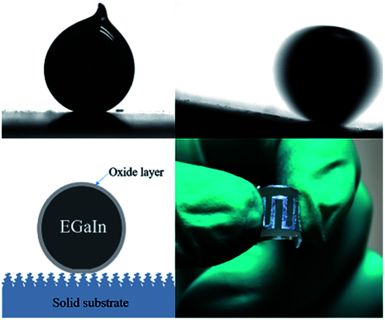
1. Introduction
Recently, flexible circuits have attracted increasing attention because of their wide applications in conductive skin, medical implants, wearable flexible devices, etc.1–6 Flexible substrates and flexible conductors play a crucial role in the flexible circuits.7,8 The emergence of flexible conductors perfectly solves the problem of the limited deformation degree that the conventional solid metal wires usually face.9,10 Liquid metal (LM) is one kind of most promising flexible conductive material that meets the requirements for flexible circuit applications.4,11–19 For example, Liu et al. prepared different flexible LM-based circuits by using the high adhesion between LM and specific soft substrates.20–22 Wu et al. designed the wettability of liquid alloy on a soft plate by UV laser roughening.23 The plate could be used to transfer liquid alloy to different substrates and make liquid alloy based soft electronic and smart systems. As an unique LM with the melting point lower than 30 °C,24,25 eutectic gallium–indium (EGaIn) has the characteristics of high conductivity,26 flexibility,11 very low vapor pressure,27 non-toxic,27 and super-cooling effect.24,28 A solid oxide thin film usually coats on the outside surface of the LM because the LM is easily oxidized in aerobic environment.29,30 It is mostly necessary to manipulate LM, such as stretching, compressing, pushing and pulling, or transporting towards the applications of LM.4,17,31–33 However, the oxide film with high adhesion makes LM easily adhere to the surface of solid materials,34 severely limiting the application range of LM. Some chemical treatments were used to remove the oxide layer and then reduce the adhesion of LM,17,35,36 but these chemical treatments are not suitable for most devices. LM is mainly applied in electronic devices and flexible equipment. Reducing the adhesion of the LM on a solid substrate is particularly important for practical applications, such as circuit printing and flexible robots. Developing a simple, non-corrosive, and universally applicable method to make various solid surfaces have excellent repellence to LM still faces significant challenge.
Herein, LM-repellent microstructures were prepared on various surfaces by femtosecond (fs) laser ablation. A liquid EGaIn droplet on the laser-treated silica glass surface has the contact angle (CA) of 157° ± 3° and the sliding angle (SA) of 10°, demonstrating excellent repellence of the laser-induced microstructure to LM. The adhesion between LM droplet and sample surfaces is very low, so the LM is difficult to adhere to the textured substrates. We defined such liquid-metal-repellent surface as “super-metal-phobic” surface. The supermetalphobicity was also achieved on the fs laser-ablated polydimethylsiloxane (PDMS), copper, and stainless steel surfaces. The surfaces exhibit stable LM repellence even though the LM droplet was heavily pressed. As a flexible conductor, the potential of designing various circuits by the LM on the laser-treated substrates was demonstrated.
2. Experimental section
Fs laser ablation was used to induce microstructure on the surfaces of different samples. The silica glass sheet (10 mm × 10 mm × 1 mm) was previously fixed on a movable platform. The fs laser with the pulse duration of 50 fs, central wavelength of 800 nm, and repetition frequency of 1 kHz was generated from a Ti: sapphire laser system (Coherent, Libra-usp 1 K-he-200). The laser beam (average power of 40 mW) was focused on the silica glass surface by an objective lens (NA = 0.45, 20×, Nikon). The moving speed of the platform was 8 mm s−1, and the interval of the adjacent laser scanning lines was set at 8 μm. Finally, the laser-treated silica glass surface was ultrasonically cleaned with absolute ethanol and deionized water for 10 minutes. Such laser processing can also be applied to many other materials to create surface microstructures, such as PDMS, copper, and stainless steel. The PDMS sheet was obtained by mixing the prepolymer and curing agent (v : v = 10 : 1) (DC-184, Dow Corning Corporation) and heated at 100 °C for 2 hours.
The surface microstructure of the samples was observed by a Flex 1000 scanning electron microscope (Hitachi, Japan). The CA and SA values of a liquid EGaIn (Shuochen Metal Co., Ltd) droplet on the sample surfaces were measured by a JC2000D contact angle system (Powereach, China). The adhesive force between LM droplet and sample surfaces was measured by a DCAT11 surface tension meter (Dataphysics, German).
3. Results and discussion
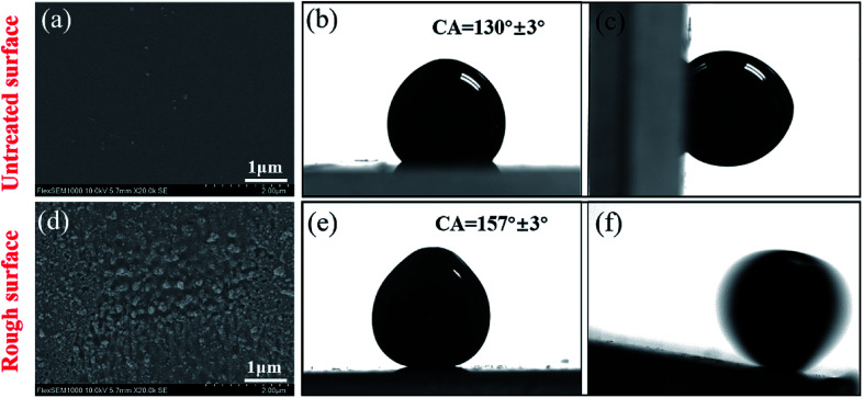
Fig. 1a and d shows the scanning electron microscopy (SEM) images of the silica glass surface before and after fs laser ablation. The surface of the untreated silica glass looks very smooth (Fig. 1a), while there are abundant protrusions with the size of hundreds of nanometers randomly distributing on the fs laser-ablated sample surface (Fig. 1d). Such microstructure is formed from the ablation-induced material removal and re-solidification of the ejected particles during fs laser ablation. When a liquid EGaIn droplet is dripped on an untreated silica glass surface, the CA of the LM droplet is 130° ± 3° (Fig. 1b). The LM droplet can firmly adhere to the silica glass surface. Even if the sample is slanted vertically, the LM droplet will not fall off (Fig. 1c). In contrast, the liquid EGaIn droplet can curl up on the laser-treated silica glass surface, with the CA of 157° ± 3° (Fig. 1e). The LM droplet will easily roll away as long as the sample surface is slightly tilted. The measured SA is only 10° (Fig. 1f). The high CA and low SA values of the LM droplet on the laser-treated rough surface indicate that the laser-induced microstructure allows the silica glass surface to have great repellence to LM. The adhesion between the LM and the silica glass is remarkably reduced after fs laser processing. Similar to the term “super-hydro-phobicity”, we use “super-metal-phobicity” to define such property that a LM droplet on the sample surface has a CA ≥ 150° and SA ≤ 10°.
Fig. 1. Surface structure and wettability of the silica glass surface before and after fs laser treatment. (a) SEM image of the untreated surface. (b) LM droplet on the untreated flat surface. (c) LM droplet adhering to the vertical untreated surface. (d) SEM image of the surface after fs laser ablation. (e) LM droplet on the laser-ablated silica glass surface. (f) LM droplet rolling on the laser-structured surface.
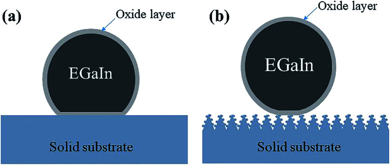
The outside of LM is generally coated with a solid oxide thin layer, so the rheology property of LM is completely different from the conventional fluids.15,23Fig. 2a depicts the state of a LM droplet on a flat substrate. The oxide layer could sufficiently touch with the substrate. The LM droplet on the flat substrate is considered at the Young contact state. High adhesion between the LM droplet and flat surface results from the large contact area, thereby LM can tightly adhere to the smooth surface. If the LM droplet is dripped on the laser-structured silica glass surface, the oxide layer first touches the peaks of the surface microstructure. The gravity is not enough to reach the yield stress that allows the densely packed microstructure on the silica glass surface to puncture the outside oxide layer, so the internal LM cannot flow out to wet the surface. In fact, the contact between the LM and the laser-treated silica glass surface is replaced by a solid–solid contact rather than liquid–solid contact. Fig. 2b shows that the LM is just in contact with the tops of the laser-induced microstructure, agreeing well with the Cassie wetting state. The surface microstructures can lead to a significant reduction of the contact area between the LM and the solid substrate, resulting in very low adhesion between the LM droplet and the laser-ablated surface. Therefore, the LM droplet is inclined to maintain a spherical shape on the rough surface and roll away easily.
Fig. 2. Wetting state of a LM droplet on different silica glass surfaces: (a) flat silica glass and (b) laser-ablated silica glass.
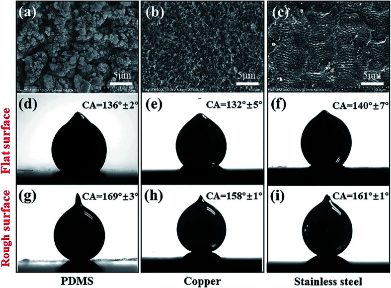
Fs laser is able to ablate almost all the known materials.37–39 Microstructures could also be induced on the surfaces of PDMS (Fig. 3a), copper (Fig. 3b), stainless steel (Fig. 3c), etc., by one-step fs laser ablation besides silica glass.40 Those surfaces were also endowed with ultralow adhesion to LM droplet. The CA values of the LM droplet on the untreated PDMS, copper, and stainless steel surfaces are only 136° ± 2° (Fig. 3d), 132° ± 5° (Fig. 3e), and 140° ± 7° (Fig. 3f), respectively. The flat surfaces also exhibit high adhesion to the LM droplet. In contrast, the CA values of LM droplet can increase to 169° ± 3° (Fig. 3g, for PDMS substrate), 158° ± 1° (Fig. 3h, for copper substrate), and 161° ± 1° (Fig. 3f, for stainless steel substrate) after fs laser processing, indicating great supermetalphobicity of the laser-ablated substrates.
Fig. 3. LM repellence of (a, d and g) PDMS, (b, e and h) copper, and (c, f, and i) stainless steel surfaces after laser treatment. (a–c) SEM images of the laser-ablated surfaces. (d–f) LM droplet on the untreated flat surfaces. (g–i) LM droplet on the laser-treated surfaces.
Table 1 shows the measured adhesive force between the LM droplet and different sample surfaces. The untreated flat substrates usually exhibit a very high adhesive force to LM droplet. Compared to the flat surfaces, the laser-induced rough microstructure enables that the adhesive force between the LM droplet and the textured sample surfaces reduces by tens to hundreds of times. For example, the adhesive force between the LM droplet and the original flat silica glass surface is 320.2 μN, while it declines to near zero for the laser-treated surface.
Adhesive force between LM droplet and different sample surfaces.
| Materials | Adhesive force (μN) | |
|---|---|---|
| Flat | Rough | |
| Silica glass | 320.2 | 1.2 |
| PDMS | 730.2 | 1.4 |
| Copper | 306.8 | 1.2 |
| Stainless steel | 257.2 | 66.8 |
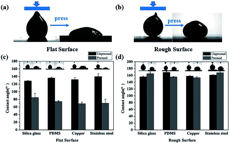
The wettability of the LM on a flat surface will inevitably change under pressure due to the easy deformation of the LM droplet, limiting the practical applications of the LM. Fortunately, the LM repellence of the structured surface is very stable even the LM droplet is pressed onto the surface. Fig. 4a and b shows the CA change of a LM droplet on the sample surface after being pressed by a force. A 7 μL LM droplet is dripped on the sample surfaces by a microsyringe. With regard to flat silica surface, the CA of the LM droplet sharply decreases from 128.4° ± 1.4° to 85° ± 11° as the LM droplet was pressed (Fig. 4a). The CA change reaches up to 43°. Such CA decline can also be observed on other untreated materials surfaces (Fig. 4c). The pressed droplet spreads on the flat surfaces with a larger contact area, so it adheres tightly to the silica glass surface. On the contrary, the LM droplet is able to keep its spherical shape on the fs laser-structured silica glass surface even though it is pressed (Fig. 4b). The change of CA value is not obvious before and after press, with just a slight shape change of the LM droplet, demonstrating a very strong and stable repellence of the laser-induced microstructure to LM. Even though a large press force of 1440 μN was acted on the LM droplet, the LM was still unable to penetrate into the laser-induced microstructure and the surface maintained remarkable LM repellence. In addition to the silica glass surface, the laser-ablated PDMS, copper, and stainless steel surfaces also show stable supermetalphobicity (Fig. 4d).
Fig. 4. CA change of a LM droplet on the sample surfaces after being pressed by a force. (a) Shape change of a LM droplet on the untreated flat silica glass surface after pressing. (b) Shape change of a LM droplet on the laser-structured silica glass surfaces. (c and d) CA change of a LM droplet on different substrates after being pressed by a force: (c) untreated flat surfaces and (d) laser-ablated surfaces.
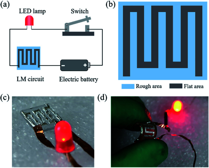
The features of high conductivity, great flexibility, and strong ductility allow the LM to have important applications in flexible electronics. Controlling the wettability of the LM on a solid substrate by fs laser treatment provides a new simple strategy for designing various circuits regardless of the substrate materials. Various circuit patterns can be directly obtained on the structured surfaces. A proof-of-concept for preparing a simple LM circuit on the laser-ablated surface was demonstrated, as shown in Fig. 5a. Part of the substrate surface was selectively ablated by fs laser to generate surface microstructure, making the rest un-ablated area form a connected pattern (Fig. 5b). When the LM was poured on the substrate surface, the repellence of the laser-induced microstructure would drive the LM to flow to the un-ablated domain. That is, the LM was restricted to just the flat pattern. As a result, a LM pattern formed on the substrate surface, which can act as a circuit. To investigate the electric continuity of the as-prepared LM circuit, it was connected with a LED lamp and a battery (Fig. 5a). As the switch was turned on and the whole circuit was connected, the LED lamp lighted up (Fig. 5c). The result demonstrates that the LM circuit has high conductivity. LM circuits can also be prepared on flexible substrates based on the similar method. As shown in Fig. 5d, LM circuit on the PDMS can maintain great conductivity even if the substrate was bent greatly. The results show that selective wetting of LM on different surfaces can provide an effective strategy for printing flexible circuits.
Fig. 5. Preparation of simple LM circuit based on fs laser-induced supermetalphobic microstructures. (a) A circuit composed of LM line, LED lamp, battery, and switch. (b) Construction of the LM circuit. (c and d) Lighting LED lamp up with the as-prepared circuit on different substrates: (c) silica glass and (d) PDMS surfaces.
4. Conclusions
Microstructure was directly fabricated on the silica glass substrate by one-step fs laser ablation. The fs laser treatment endows the silica glass surface with great repellence to LM. A LM droplet on the structured surface has a CA of 157° ± 3° and SA of 10°. Compared to the untreated flat surface, the adhesive force between LM droplet and the laser-ablated silica glass surface is reduced from 320.2 μN to 1.2 μN. The PDMS, copper, and stainless steel surfaces also show ultralow adhesion to LM after fs laser ablation besides silica glass. The solid–solid (oxide layer-substrate) contact between the LM and solid surface replaces the original liquid–solid contact, resulting in the Cassie wetting state between the LM droplet and the laser-induced microstructure. The repellent property makes the LM be hard to adhere to the laser-structured surface. The supermetalphobic microstructure enables us to obtain LM patterns on a solid substrate, which can be used as a circuit. By taking advantages of high conductivity and flexibility, we believe that the laser-induced supermetalphobic microstructures have important potential applications in flexible electronics.
Conflicts of interest
No conflicts of interest in this article.
Supplementary Material
Acknowledgments
This work is supported by the National Key Research and Development Program of China under the grant no. 2017YFB1104700, the National Science Foundation of China under the grant no. 61875158, U1630111, and 61805192, the Fundamental Research Funds for the Central Universities.
References
- Kim S. Y. Baines R. Booth J. Vasios N. Bertoldi K. Kramer-Bottiglio R. Nat. Commun. 2019;10:3464. doi: 10.1038/s41467-019-11294-7. [DOI] [PMC free article] [PubMed] [Google Scholar]
- Wang S. Xu J. Wang W. Wang G. N. Rastak R. Molina-Lopez F. Chung J. W. Niu S. Feig V. R. Lopez J. Lei T. Kwon S. K. Kim Y. Foudeh A. M. Ehrlich A. Gasperini A. Yun Y. Murmann B. Tok J. B. Bao Z. Nature. 2018;555:83–88. doi: 10.1038/nature25494. [DOI] [PubMed] [Google Scholar]
- Chen X. Rogers J. A. Lacour S. P. Hu W. Kim D. H. Chem. Soc. Rev. 2019;48:1431–1433. doi: 10.1039/C9CS90019E. [DOI] [PubMed] [Google Scholar]
- Kamyshny A. Magdassi S. Chem. Soc. Rev. 2019;48:1712–1740. doi: 10.1039/C8CS00738A. [DOI] [PubMed] [Google Scholar]
- Kim M.-g. Alrowais H. Pavlidis S. Brand O. Adv. Funct. Mater. 2017;27:1604466. doi: 10.1002/adfm.201604466. [DOI] [Google Scholar]
- Biswas S. Schoeberl A. Hao Y. Reiprich J. Stauden T. Pezoldt J. Jacobs H. O. Nat. Commun. 2019;10:4909. doi: 10.1038/s41467-019-12870-7. [DOI] [PMC free article] [PubMed] [Google Scholar]
- Tavakoli M. Malakooti M. H. Paisana H. Ohm Y. Marques D. G. Alhais Lopes P. Piedade A. P. de Almeida A. T. Majidi C. Adv. Mater. 2018;30:1801852. doi: 10.1002/adma.201801852. [DOI] [PubMed] [Google Scholar]
- Shintake J. Cacucciolo V. Floreano D. Shea H. Adv. Mater. 2018;30:1707035. doi: 10.1002/adma.201707035. [DOI] [PubMed] [Google Scholar]
- Liang S. Li Y. Chen Y. Yang J. Zhu T. Zhu D. He C. Liu Y. Handschuh-Wang S. Zhou X. J. Mater. Chem. C. 2017;5:1586–1590. doi: 10.1039/C6TC05358K. [DOI] [Google Scholar]
- Li G. Lee D. W. Lab Chip. 2017;17:3415–3421. doi: 10.1039/C7LC00768J. [DOI] [PubMed] [Google Scholar]
- Dickey M. D. Adv. Mater. 2017;29:1606425. doi: 10.1002/adma.201606425. [DOI] [PubMed] [Google Scholar]
- Chen Y. Liu Z. Zhu D. Handschuh-Wang S. Liang S. Yang J. Kong T. Zhou X. Liu Y. Zhou X. Mater. Horiz. 2017;4:591–597. doi: 10.1039/C7MH00065K. [DOI] [Google Scholar]
- Boley J. W. White E. L. Chiu G. T. C. Kramer R. K. Adv. Funct. Mater. 2014;24:3501–3507. doi: 10.1002/adfm.201303220. [DOI] [Google Scholar]
- Wang Q. Yu Y. Yang J. Liu J. Adv. Mater. 2015;27:7109–7116. doi: 10.1002/adma.201502200. [DOI] [PubMed] [Google Scholar]
- Hirsch A. Dejace L. Michaud H. O. Lacour S. P. Acc. Chem. Res. 2019;52:534–544. doi: 10.1021/acs.accounts.8b00489. [DOI] [PubMed] [Google Scholar]
- Ma B. Xu C. Chi J. Chen J. Zhao C. Liu H. Adv. Funct. Mater. 2019;29:1901370. doi: 10.1002/adfm.201901370. [DOI] [Google Scholar]
- Moorefield M. R. Gough R. C. Ohta A. T. Shiroma W. A. IEEE Access. 2018;6:1261–1266. [Google Scholar]
- Li X. Li M. Xu J. You J. Yang Z. Li C. Nat. Commun. 2019;10:3514. doi: 10.1038/s41467-019-11466-5. [DOI] [PMC free article] [PubMed] [Google Scholar]
- Ozutemiz K. B. Wissman J. Ozdoganlar O. B. Majidi C. Adv. Mater. Interfaces. 2018;5:1701596. doi: 10.1002/admi.201701596. [DOI] [Google Scholar]
- Zheng Y. He Z. Gao Y. Liu J. Sci. Rep. 2013;3:1786. doi: 10.1038/srep01786. [DOI] [Google Scholar]
- Gao Y. Li H. Liu J. PLoS One. 2013;8:e69761. doi: 10.1371/journal.pone.0069761. [DOI] [PMC free article] [PubMed] [Google Scholar]
- Guo R. Tang J. Dong S. Lin J. Wang H. Liu J. Rao W. Adv. Mater. Technol. 2018;3:1800265. doi: 10.1002/admt.201800265. [DOI] [Google Scholar]
- Zhang S. Wang B. Jiang J. Wu K. Guo C. F. Wu Z. ACS Appl. Mater. Interfaces. 2019;11:7148–7156. doi: 10.1021/acsami.8b20595. [DOI] [PubMed] [Google Scholar]
- Daeneke T. Khoshmanesh K. Mahmood N. de Castro I. A. Esrafilzadeh D. Barrow S. J. Dickey M. D. Kalantar-Zadeh K. Chem. Soc. Rev. 2018;47:4073–4111. doi: 10.1039/C7CS00043J. [DOI] [PubMed] [Google Scholar]
- Joshipura I. D. Ayers H. R. Majidi C. Dickey M. D. J. Mater. Chem. C. 2015;3:3834–3841. doi: 10.1039/C5TC00330J. [DOI] [Google Scholar]
- Cheng S. Wu Z. Lab Chip. 2012;12:2782–2791. doi: 10.1039/C2LC21176A. [DOI] [PubMed] [Google Scholar]
- Liu T. Sen P. Kim C.-J. J. Microelectromech. Syst. 2012;21:443–450. [Google Scholar]
- Ottaviano L. Filipponi A. Di Cicco A. Phys. Rev. B: Condens. Matter Mater. Phys. 1994;49:11749–11758. doi: 10.1103/PhysRevB.49.11749. [DOI] [PubMed] [Google Scholar]
- Larsen R. J. Dickey M. D. Whitesides G. M. Weitz D. A. J. Rheol. 2009;53:1305–1326. doi: 10.1122/1.3236517. [DOI] [Google Scholar]
- Li X. Li M. Zong L. Wu X. You J. Du P. Li C. Adv. Funct. Mater. 2018;28:1804197. doi: 10.1002/adfm.201804197. [DOI] [Google Scholar]
- Baek S. Park U. Choi I. H. Kim J. J. Micromech. Microeng. 2013;23:055006. doi: 10.1088/0960-1317/23/5/055006. [DOI] [Google Scholar]
- Wissman J. Dickey M. D. Majidi C. Adv. Sci. 2017;4:1700169. doi: 10.1002/advs.201700169. [DOI] [PMC free article] [PubMed] [Google Scholar]
- Won D.-J. Baek S. Huh M. Kim H. Lee S. Kim J. Sens. Actuators, A. 2017;259:105–111. doi: 10.1016/j.sna.2017.03.032. [DOI] [Google Scholar]
- Kadlaskar S. S. Yoo J. H. Abhijeet Lee J. B. Choi W. J. Colloid Interface Sci. 2017;492:33–40. doi: 10.1016/j.jcis.2016.12.061. [DOI] [PubMed] [Google Scholar]
- Bilodeau R. A. Zemlyanov D. Y. Kramer R. K. Adv. Mater. Interfaces. 2017;4:1600913. doi: 10.1002/admi.201600913. [DOI] [Google Scholar]
- Khan M. R. Eaker C. B. Bowden E. F. Dickey M. D. Proc. Natl. Acad. Sci. U. S. A. 2014;111:14047–14051. doi: 10.1073/pnas.1412227111. [DOI] [PMC free article] [PubMed] [Google Scholar]
- Sugioka K. Cheng Y. Light: Sci. Appl. 2014;3:e149. doi: 10.1038/lsa.2014.30. [DOI] [Google Scholar]
- Bai X. Yang Q. Fang Y. Zhang J. Yong J. Hou X. Chen F. Chem. Eng. J. 2020;383:123143. doi: 10.1016/j.cej.2019.123143. [DOI] [Google Scholar]
- Li M. Yang Q. Chen F. Yong J. Bian H. Wei Y. Fang Y. Hou X. Adv. Eng. Mater. 2019;21:1800994. doi: 10.1002/adem.201800994. [DOI] [Google Scholar]
- Yong J. Zhan Z. Singh S. C. Chen F. Guo C. Langmuir. 2019;35:9318–9322. doi: 10.1021/acs.langmuir.9b01063. [DOI] [PMC free article] [PubMed] [Google Scholar]


