Abstract
This paper studies the performance of a gas sensor based on an organic/inorganic diode for ammonia (NH3), nitrogen (N2) & oxygen (O2) sensing under atmospheric conditions at room temperature and different humidity levels. The diode structure consists of a layer of different kinds of polymer (PTFE, PVDF, PANI) deposited on top of BiVO4. The polymer layer, which is filled with different ratios of graphene oxide (GO), is prepared from the solution phase. We show that the current–voltage (I–V) response of the diode and the sensing performance are improved significantly by adding GO to the polymer layer. The sensing response is highest for a diode with 0.04 wt% of GO. At room temperature, the poly-GO (0.04 wt%)/BiVO4 Schottky diode shows a sensitivity of 194 ppm upon exposure to 20 ppm of NH3 in ambient air with rapid response and recovery times between 95 and 101 s, respectively. The sensor based on the polymer–GO diode is cost-effective, environmentally friendly, and easy to fabricate using low-cost solution-processing methods.
This paper studies the performance of a gas sensor based on an organic/inorganic diode for ammonia (NH3), nitrogen (N2) & oxygen (O2) sensing under atmospheric conditions at room temperature and different humidity levels.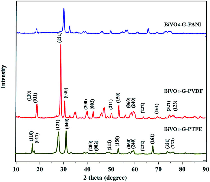
Introduction
Ammonia has been widely used in agricultural, medical, and industrial applications.1,2 NH3 is a colorless and toxic gas that can cause severe problems for human health. On the other hand, N2 & O2 has been detected for comparison with NH3 gas. To measure NH3 in the atmosphere, fabricating an efficient and reliable NH3 sensor that has a high sensitivity, rapid detection response, and rapid recovery time is essential. Solid-state NH3 gas sensors have been the focus of recent research.3,4 Schottky diode heterojunctions are promising candidates for sensing a low concentration of gases, since upon gas exposure, a small change in the chemical composition of the layers, contact barriers, or even the interfaces can lead to a huge difference in the diode response or current–voltage (I–V) characteristics.2,4–7 Recently, Chen et al. have reported a Pt/AlGaN/GaN Schottky diode that detects NH3 at 35 ppm with a response time approaching 7 min and a sensitivity of 13.1.4 However, the reported high sensitivity was achieved at elevated temperatures, 50 °C (423 K) instead of room temperature. A Schottky diode-type ammonia sensor with high sensitivity, rapid detection response and rapid recovery time is still required. Other kinds of polymer (PTFE, PVDF, PANI) include conducting polymers with high conductivity, environmental stability, optical transparency, and moderate redox potential.8–14 Recently, gas sensors based on PTFE, PVDF, or PANI have been introduced as promising gas detectors with efficient properties, such as a facile fabrication process, low cost, high sensitivity, and fast response time.3,15,16 It is well-known that (PTFE, PVDF, PANI) are conductive polymers with high stability in air, suggesting their potential in sensing applications. For instance, Lin et al. fabricated a nitric oxide (NO) gas sensor by using a (PTFE, PVDF, PANI) modified electrode.17 However, the response and recovery time were long, about a few minutes.17 Mixing (PTFE, PVDF, PANI) with carbon nanostructures, such as graphene sheets (and its derivatives), creates a composite material with stronger mechanical strength and better electrical properties because of its high surface to volume ratio.8–14 Water-soluble graphene oxide (GO) has a unique heterogeneous electronic structure because of the presence of mixed sp2 and sp3 hybridizations.9,18–20 Poly-GO composites have been recently employed as electrical contacts in organic solar cells9,21,22 and light-emitting diodes,18,20 as an electrode in batteries,23,24 within the hydrogen evolution reaction,25 as supercapacitors,26 as gas and chemical sensors27–32 and as transistors.33 For sensing applications, poly-GO composites hold great promise because of the large surface area of the GO flakes.9–13 The GO sheets provide a better platform to absorb the target gas and to provide electron transfer within the conductive network of (PTFE, PVDF, PANI). Besides the absorption of gas on the surface of the hybrid layer, the interfaces between the composite and semiconductor in diode-based gas sensors can be used in the detection of gas, leading to a higher response than with pure (PTFE, PVDF, PANI) based gas sensors. Here, we mixed GO sheets in different concentrations with (PTFE, PVDF, PANI) water-based suspensions and used the composite as an ammonia-sensing layer in a BiVO4 Schottky diode. The GO sheets were prepared by a modified Hummer’s method.20,34,35 The diode parameters and sensing performance improved by adding an infinitesimal amount of GO into (PTFE, PVDF, PANI). At a low GO loading of 0.04 wt% in (PTFE, PVDF, PANI), the diode showed a sensitivity of 194 to 201 ppm ammonia in the atmosphere at room temperature (25 °C), with a response and recovery time of 95 and 121 s, respectively. In this work, a new class of high electron mobility Schottky diode gas sensor is presented as a chemical sensing platform with high performance, good stability, low limit of detection down to ppb level and functionality at room temperature. The key components in our design of the device are a Schottky contact material on an organic/inorganic diode formed by different kinds of polymer (PTFE, PVDF, PANI) deposited on top of BiVO4. Gas sensors based on GO have shown high sensitivity at room temperature and rapid response. The sensing mechanism of the device in this work is based on the coupling effect between the GO nanosheets and the (PTFE, PVDF, PANI) deposited on top of BiVO4 surface, while the GO nanosheets showed p-type characteristics mainly caused by exposure to the ambient environment and their van der Waals heterostructure with the polymer layers, forming a Schottky diode with BiVO4. When the diode sensors were introduced to NH3 gases for investigation of their sensor response, the Schottky diode sensor with an organic/inorganic diode formed by different kinds of polymer (PTFE, PVDF, PANI) deposited on top of BiVO4 responded more rapidly and strongly to NH3 gases, down to ppb levels. This heterostructuring of a GO active Schottky diode based on an organic/inorganic diode formed by different kinds of polymer (PTFE, PVDF, PANI) deposited on top of BiVO4 sensing layer will form the next generation of gas sensor applications. Due to its gas detection capabilities at room temperature, the Schottky diode gas sensor has great potential for integration into portable wireless electronic systems for a variety of applications.
Experimental
Graphite flakes, hydrogen peroxide, potassium permanganate (KMnO4), and poly(3,4-ethylenedioxythiophene):poly(styrenesulfonate) (PTFE, PVDF, PANI), 1.3 wt% dispersion in H2O, conductive grade, pH 10 were purchased from Sigma Aldrich. Sulfuric acid, hydrochloric acid, (NH3, N2, O2), methanol, ethanol, acetone, and dimethyl sulfoxide (DMSO) were purchased from Merck and used without any purification. GO was synthesized using a modified Hummer’s method with expanded graphite.18,19 The obtained GO was diluted in deionized water (1 mg ml−1). The solution was then sonicated for 20 min in a bath sonicator, followed by centrifugation at 5000 rpm for 5 min. The GO sheets produced with this procedure had a lateral size of 60 mm. After filtration of (PTFE, PVDF, PANI) (0.5 mm pore size), different concentrations of GO (0.00, 0.02, 0.04, 0.06, and 0.08 wt%) along with 6 wt% of dimethyl sulfoxide (DMSO) were added and stirred for 6 h. The device structure of the poly-GO/BiVO4 gas sensor is illustrated in Fig. 1a. Ohmic back contacts to the BiVO4 wafer (1 × 1 cm2) (with impurity concentration of 1.5 × 10¹⁸ atoms cm3) were made using Au–Ge alloy (100 nm) physical vapor deposition on the reverse side of the BiVO4 wafers. The back contacts were then annealed at 350 °C under a nitrogen atmosphere for 3 min. Poly-GO with different GO loading ratios (0.02, 0.04, 0.06, 0.08 wt%), were spin-coated on the top surface of n-type epitaxial BiVO4. The comparison BiVO4 was cleaned prior to poly-GO deposition using Piranha solution. The devices were then dried for 60 min in a furnace (Exciton, EX1200-4L) at 80 °C under a nitrogen atmosphere. Ohmic top metal contacts were then made by vacuum evaporation (10−5 mbar) of silver (200 nm) on top of the active layer. Freeze-dried GO samples were examined with scanning electron microscopy (SEM, JEOL-6390). Transmission electron microscopy (TEM) images were obtained using a JEM-2200 FS at 200 kV. Fourier-transform infrared spectroscopy (FTIR) analysis was performed using a Bruker, IFS-66/S over the wavenumber range of 4000–400 per cm. X-Ray diffraction (XRD) studies were performed to characterize the interlayer spacing of the GO samples using a powder XRD system (Philips1825) with Cu Kα radiation (λ 1/4 0.154 nm), operating at 40 keV and with a cathode current of 20 mA. The thickness of the poly-GO thin films was obtained by SEM cross-section measurements. The sensors were placed inside a home-made test chamber, as schematically illustrated. The chamber was connected to a mixer where the ammonia gas and highly purified nitrogen (99%) were mixed. Mass flow controllers (MFC, Alicat Scientific, Tucson, AZ, USA) were used to modulate the flow rates of ammonia and nitrogen. The I–V measurements of the sensors were made using a Keithley 238 high current source measure unit. The forward biased I–V characteristics of the junction before and after exposure to NH3 were recorded. The maximum current change at a fixed voltage (þ 1.5 V) was used to determine the sensitivity of the sensors. The sensitivity was defined using sensitivity ¼Iair/Igas, by measuring the currents of the poly-GO/BiVO4 heterojunction in air and in the presence of NH3. The standard experiments were carried out at room temperature (25 °C) and a relative humidity of 15%.
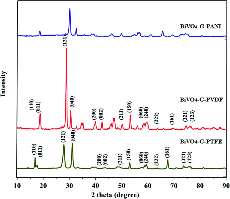
Fig. 1. XRD data of BiVO4–GO–PTFE; BiVO4–GO–PVDF and BiVO4–GO–PANI sample.
Characterization of GO sheets
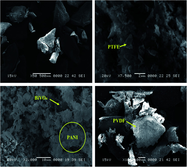
The XRD spectrum of the as-prepared GO is given in Fig. 1. The sharp peak at 2θ = 10.1 confirms the d-spacing of 8.78 Å, thereby suggesting that the GO sheets are interlinked via functional (carboxyl and hydroxyl) groups. Fig. 2b shows the FTIR spectra of the prepared GO. The vibration modes of the GO sample were assigned in accordance with previously reported work.16,21 The characteristic peaks of the as-prepared GO were assigned at 3423 cm−1 (O–H stretching vibrations are assigned to the hydroxyl groups on the GO surface), 1742 cm−1 (C55O groups in carbonyl and carboxyl moieties), 1631 cm−1 (skeletal vibrations of unoxidized graphitic domains (C55C)), 1416 cm−1 (C–O carboxy), 1220 cm−1 (C–O epoxy), and 1150 cm−1 (C–O stretching vibrations).16,21 An SEM image of the as-prepared GO is given in Fig. 2. The depicted GO sheets were measured to have a lateral size in the range of 40–80 μm. However, smaller fragments of GO sheet with a lateral size between 20–30 μm were also observed. According to the cross-section image of the Schottky diode the thickness of the (PTFE, PVDF, PANI)–GO is almost 950 nm.
Fig. 2. SEM image of (a) BiVO4–GO–PVDF; (b) BiVO4–GO–PTFE and (c) BiVO4–GO–PANI (d) BiVO4–GO–PVDF sample.
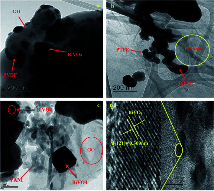
In addition, such an amorphous structure is also revealed by TEM investigation, as shown in Fig. 3. This poly-GO–BiVO4 was found to actually consist of many smaller nanoparticles with a size of about 50 nm. TEM imagery (Fig. 3) was recorded on the edge of the nanoparticle. The clear lattice fringe specifies the high-crystallinity and single-crystalline behaviour of the nanoparticles. The interplanar spacing is 0.309 nm, which corresponds to the (121) plane of monoclinic BiVO4. It has also been reported that small grain size and high crystallinity endowed increased photocatalytic activity for increased reactive sites, and promoted electron–hole separation efficiency. Thus, the as-prepared nano poly-GO–BiVO4 was expected to show enhanced sensing performance.
Fig. 3. TEM & HRTEM image of (a) BiVO4–GO–PVDF; (b) BiVO4–GO–PTFE and (c) BiVO4–GO–PANI (d) HRTEM image.
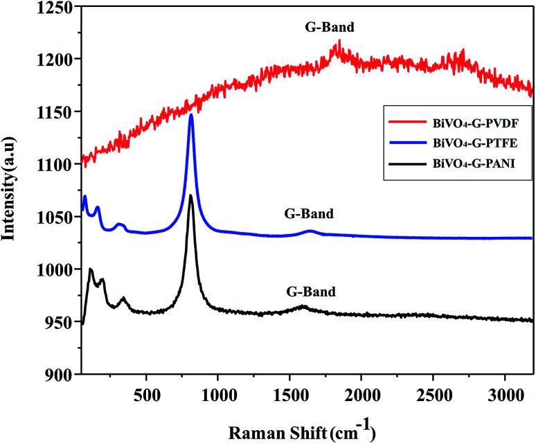
Raman spectroscopy is one of the most helpful tools to characterize carbon-based materials. Fig. 4 shows the Raman spectra of selective poly-BiVO4–GO composites (a) BiVO4–GO–PVDF; (b) BiVO4–GO–PTFE and (c) BiVO4–GO–PANI. Consistent with the XRD results, the Raman spectra show that BiVO4 has a monoclinic phase, on the basis of the characteristic stretching vibrations and bending vibrations of the VO43− tetrahedron. The Raman spectrum of PANI–BiVO4–GO demonstrates one characteristic band at 1600 cm−1, corresponding to the G band of GO, accordingly. In comparison, the BiVO4–GO–PTFE and BiVO4–GO–PVDF composites show that the G band is a little red shifted to 1606 cm−1 which may, accordingly, be caused by the changed surface strain, due to the contact between GO and BiVO4. This phenomenon is consistent with that observed in the hydrothermal in situ preparation of the poly-BiVO4–GO composites, where a D/G ratio close to zero suggests the effective combination of BiVO4–GO with PANI polymer and others.
Fig. 4. TEM & HRTEM image of (a) BiVO4–GO–PVDF; (b) BiVO4–GO–PTFE and (c) BiVO4–GO–PANI.
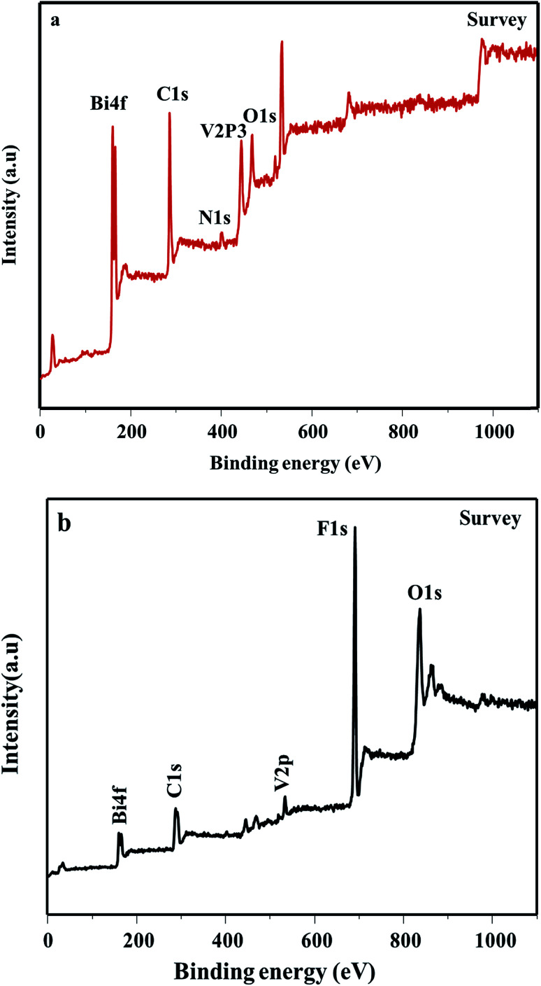
The composition of the poly-BiVO4–GO heterogeneous nanostructures has been further investigated using X-ray photoelectron spectroscopy (XPS). Fig. 5 shows the high-resolution XPS spectra of the as-prepared poly-BiVO4–GO heterogeneous nanostructures. Fig. 5a shows that the binding energies are located at about (160.1 and 166.5) eV, corresponding to the Bi4f5/2 and Bi4f7/2 bands, respectively. The XPS spectrum of the O1s band, indicating that different oxygen species exist on the surface of PANI–BiVO4–GO heterogeneous nanostructures. The binding energies located at about (532.2 and 533.1) eV are ascribed to the O1s band of the lattice oxygen of GO crystallites and the O1s band of the lattice oxygen of BiVO4 crystallites, respectively. In the high-resolution XPS spectrum of the V2p band, the peaks at about (527 and 518.5) eV correspond to V2p1/2 and V2p3/2 bands, respectively. The XPS spectrum of the C1s band presented in Fig. 5a, clearly shows one peak located at 287.3 eV, which corresponds to the C1s bands of GO and PANI crystallites, respectively. The C1s peak is accompanied by two satellites that are evident on the high-binding-energy side, denoted as peaks I and II, which are located at about (287.3 and 287.5) eV, respectively. The main peak in the XPS spectrum of the N1s band is known to be characteristic of N2−; the shake-up satellite peaks are evident, and are diagnostic of an open 3p4 shell of the N2− state, indicating the presence of PANI at the surface. The fact that XRD does not show evidence of a PANI phase while XPS shows the surface presence of N2− ions suggests that –NH2 is present only on the surface of the PANI nanocrystals, and forms a very thin amorphous outer shell. On the basis of the above experimental results of XRD, TEM, and XPS, it can be deduced that the N element exists in the form of NH− on the surface of PANI–BiVO4–GO heterogeneous nanostructures.
Fig. 5. XPS data of (a) BiVO4–GO–PANI & (b) BiVO4–GO–PVDF.
I–V characteristics of the poly-GO/BiVO4 Schottky diode
The forward bias I–V characteristics of the poly-GO–BiVO4 Schottky diodes fabricated with different GO contents show a decent rectifying behavior. The forward bias increases via doping the (PTFE, PVDF, PANI) solution with different amounts of GO. The maximum forward bias current was measured for 0.04 wt% GO, which shows the highest conductivity. However, if one adds an excessive amount of GO, up to 0.40 wt%, the diode behavior degrades. The observed behavior in diode performance can be rationalized via changing the conductivity of (PTFE, PVDF, PANI) by adding GO. The conductivity increases with the addition of GO, reaches a maximum value at 0.04 wt%, and drops by further addition of GO (as will be explained in detail in the next section). Therefore, because of the reduction of conductivity at higher loading, the diode performance deteriorates.
Ammonia-sensing properties
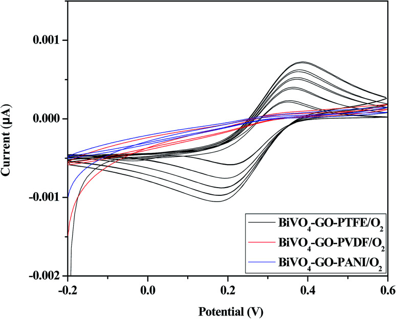
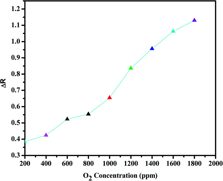
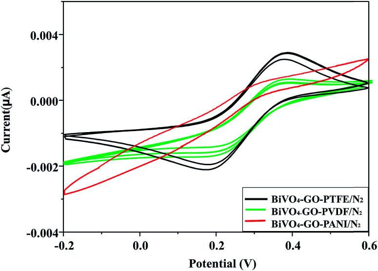
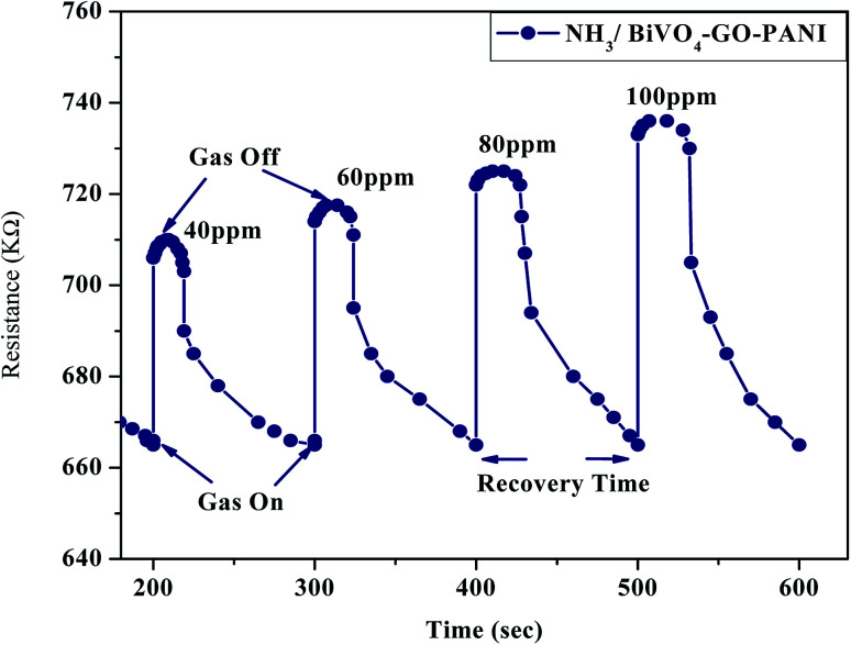
The NH3 response of the poly-GO/BiVO4 Schottky diode at an applied potential of þ 1.5 V is shown in Fig. 6. The diode at 0 wt% GO showed a weak response in sensitivity when exposed to different NH3 concentrations. However, as the concentration of GO increased to 0.04 wt%, the sensitivity of the diode increased. Upon further increasing of GO in the (PTFE, PVDF, PANI) solution, the sensitivity dropped again to the level of pristine (PTFE, PVDF, PANI). The sensitivity value of the poly-GO (0.04 wt%)/BiVO4 heterojunction was measured to be 3654 in 1800 ppm NH3, which is nearly two times higher than the pristine (PTFE, PVDF, PANI). The conductivity of the sensing layer as a function of GO concentration is shown in Fig. 7. This improvement in sensitivity is attributed to the increase in conductivity with added GO (0.04 wt%) nanosheets from 650 (S cm−1) in 0 wt% GO to 950 (S cm−1) in 0.04 wt% (Fig. 8). The reason for the increase in conductivity as well as the morphological study was given in detail.20,36 Briefly, because of several functional groups (such as –COOH and –OH) on GO nanosheets, positively charged PTFE, PVDF, PANI chains adsorb on the surface of GO nanosheets. The absorption of PTFE, PVDF, PANI chains induces a phase separation between PTFE, PVDF, PANI chains, which enlarges the PTFE, PVDF, PANI domain (Fig. 9). Moreover, as a result of coulombic repulsions among the positive charges in the PTFE, PVDF, PANI chains adsorbed on the surface of the GO, PTFE, PVDF, PANI chains form a linear conformation which increases the number of active sites available to the analyte (Fig. 10).20,36 In addition, the formation of linear PTFE, PVDF, PANI chains and the phase separation between PTFE, PVDF, PANI enlarge the PTFE, PVDF, PANI-rich domains with longer conductive pathways, leading to an increase in carrier mobility. On the other hand, by further increasing the GO content (more than 0.04 wt%), more functional groups on GO sheets can bond with fewer PTFE, PVDF, PANI chains by coulombic attraction. Thus, because there are fewer PTFE, PVDF, PANI chains distributed in GO nanosheets, the coulombic repulsions between the positive charges in the PTFE, PVDF, PANI chains are reduced. As a result of less coulombic repulsion, the PTFE, PVDF, PANI chains on the surface of GO again form a coil structure (Fig. 10). Therefore, the carrier mobility and the number of available active sites for interacting with analyte molecules will decrease and the performance of the (NH3, N2, O2) sensor will diminish. Indeed, the concentration of GO in (PTFE, PVDF, PANI) has an important role in the performance of the sensor. Moreover, the addition of GO into (PTFE, PVDF, PANI) has a synergistic effect that increases the response to (NH3, N2, O2). In our previous work, we investigated the sensing mechanism of (PTFE, PVDF, PANI)–GO exposed to volatile organic compound (VOC) gases.16 Briefly, the NH3 gas molecule acts like an electron donor. When the (PTFE, PVDF, PANI)–GO sensing layer is exposed to an electron donor (like an NH3 molecule), the charge carriers (holes) in a p-type semiconductor like (PTFE, PVDF, PANI)–GO decrease, increasing film resistivity. In addition, NH3 molecules interact not only with the (PTFE, PVDF, PANI) and GO, but also by π–π bonding interactions between GO and (PTFE, PVDF, PANI). The interaction between (NH3, N2, O2) polar molecules and (PTFE, PVDF, PANI)–GO leads to a charge transfer across delocalized π electrons, resulting in the measured improved gaseous detection properties.16,20 In the next step, room-temperature I–V characteristics of the (PTFE, PVDF, PANI)–GO (0.04 wt%)/BiVO4 heterojunction at different concentrations (ppm) of NH3 were measured, as presented in Fig. 11. The (NH3, N2, O2) concentration was varied systematically between 200–1800 ppm. The sensor response (%) versus (NH3, N2, O2) concentration was extracted from Fig. 11. The sensor response increased from 26 to 3654 with increasing NH3 concentration from 200 to 1800 ppm. The detection limit of (NH3, N2, O2) for the poly-GO (0.04 wt%)/BiVO4 heterojunction gas sensor was thus estimated to be 200 ppm at the room temperature. As the (NH3, N2, O2) concentration reaches 1800 ppm, the response of the sensor saturates, because of the chemical nature of NH3 and the reaction products, which may not diffuse away from the interface immediately upon completion of the reaction.3,5 The response time of the sensor is shown in Fig. 12. The time-dependent response was measured at a constant voltage of 1.5 V. The resistance difference (ΔR) with different concentrations of NH3 gas (40, 60, 80 and 100 ppm) is illustrated in Fig. 12. The maximum sensitivity is reached within 8 seconds, and the recovery time approaches 101 seconds.
Fig. 6. Optimal manufacturing process for the polymer-based gas-sensor. Cyclic voltammogram of BiVO4–GO–PTFE/O2; BiVO4–GO–PVDF/O2 and BiVO4–GO–PANI/O2 after flowing O2 gas.
Fig. 7. Concentration dependence of the electrical response (ΔR) for BiVO4–GO–PANI sample in response to increasing levels of O2 concentration (ppm).
Fig. 8. Optimal manufacturing process for the polymer-based gas-sensor. Cyclic voltammogram of BiVO4–GO–PTFE/N2; BiVO4–GO–PVDF/N2 and BiVO4–GO–PANI/N2 after flowing N2 gas.
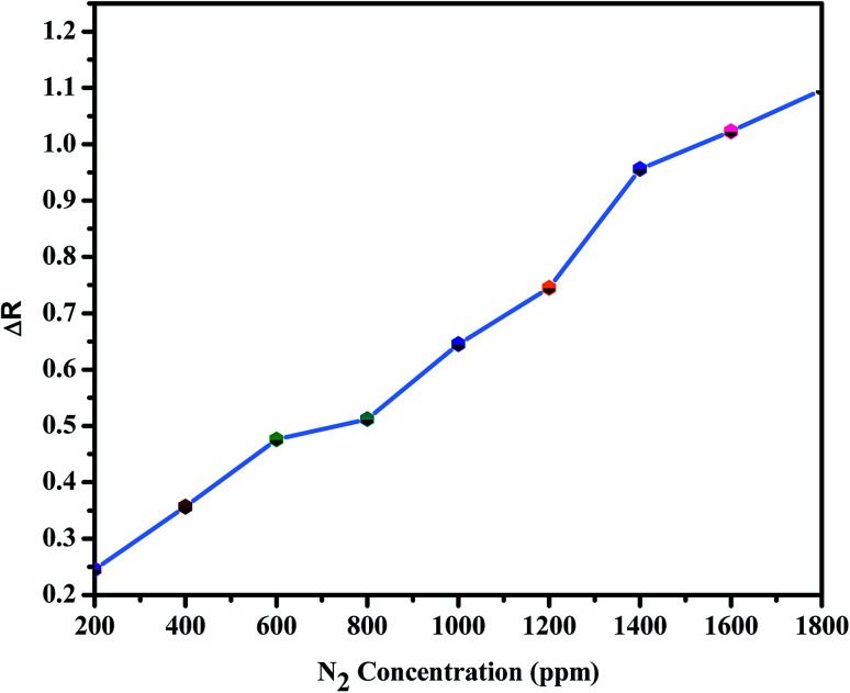
Fig. 9. Concentration dependence of the electrical response (ΔR) for BiVO4–GO–PANI sample in response to increasing levels of N2 concentration (ppm).
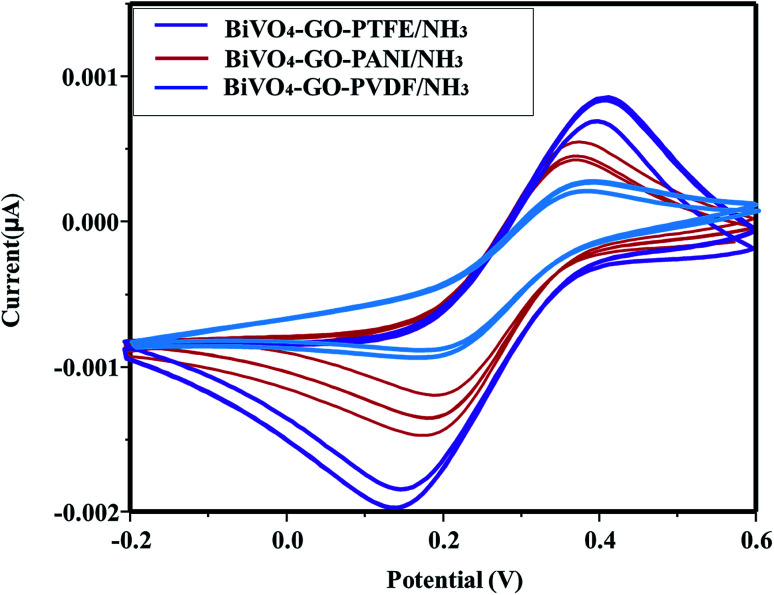
Fig. 10. Optimal manufacturing process for the polymer-based gas-sensor. Cyclic voltammogram of BiVO4–GO–PTFE/NH3; BiVO4–GO–PANI/NH3 and BiVO4–GO–PVDF/NH3 after flowing NH3 gas.
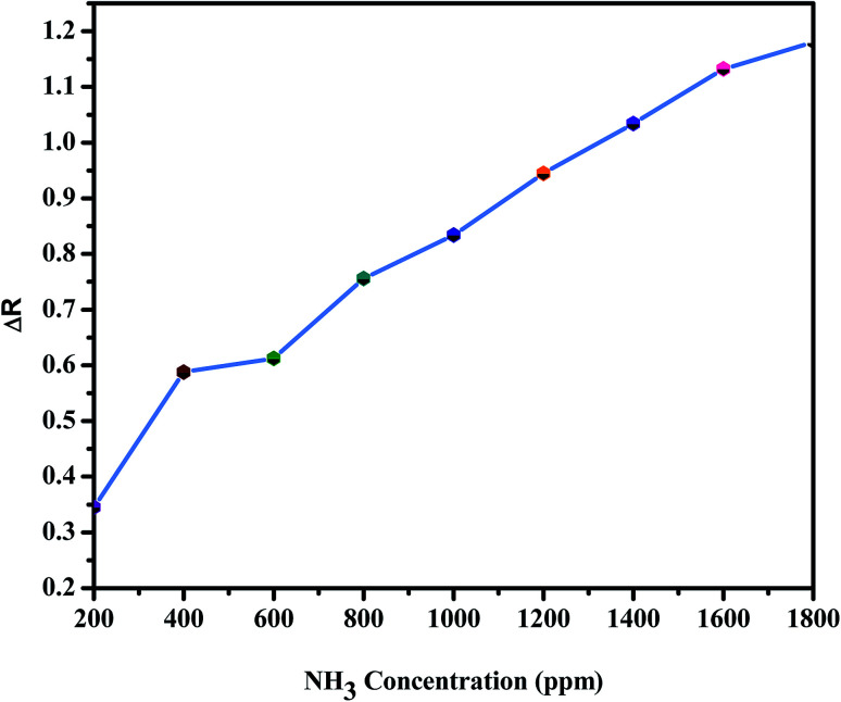
Fig. 11. Concentration dependence of the electrical response (ΔR) for BiVO4–GO–PVDF sample in response to increasing levels of NH3 concentration (ppm).
Fig. 12. Dynamic response of the BiVO4–GO–PANI gas sensor with different concentration of NH3 gas.
Temperature effects
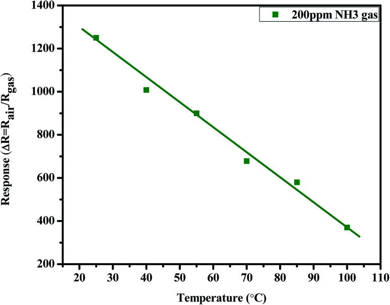
Compared to metal oxide-based gas sensors,34,37,38 the poly-GO thin-film gas sensors operate at lower temperatures. The temperature response of the sensor for 200 ppm NH3 is given in Fig. 13. The interaction between the poly-GO thin film and NH3 is exothermic; hence the activation energy of desorption is larger than that of the adsorption.35 The increase in temperature facilitates both gas adsorption and desorption, but favors the process with a higher activation energy.17,39–41 Therefore the observation of a longer recovery time, as well as the decrease in response at higher temperatures, is attributed to a high NH3 desorption rate.15,42,43
Fig. 13. Effect of temperature on the NH3 gas sensing response of the BiVO4–GO (0.04 wt%)–PANI Schottky diode sensor.
Stability
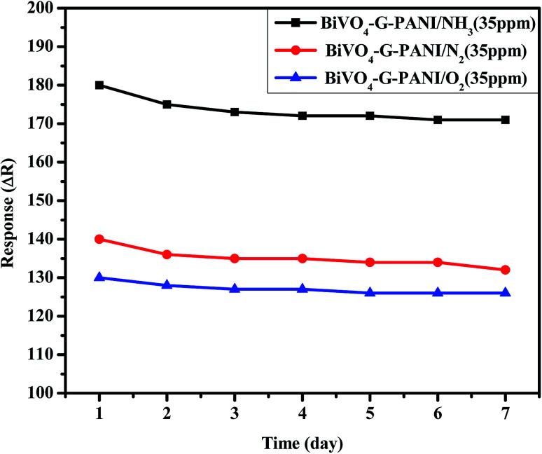
Fig. 14 indicates the stability of the poly-GO (0.04 wt%)/BiVO4 gas sensor exposed to 35 ppm NH3, N2, O2 for 7 days at room temperature (25 °C and 17% RH). The response of the gas sensor slightly decreases from 181 to 175 after 4 days, and it remains almost unchanged for three days. Therefore, the stability of the sensor is quite good and enables long-term application.
Fig. 14. Stability of the gas sensor exposed to 35 ppm NH3, N2, O2 gases, with the BiVO4–G–PANI sample.
Selectivity
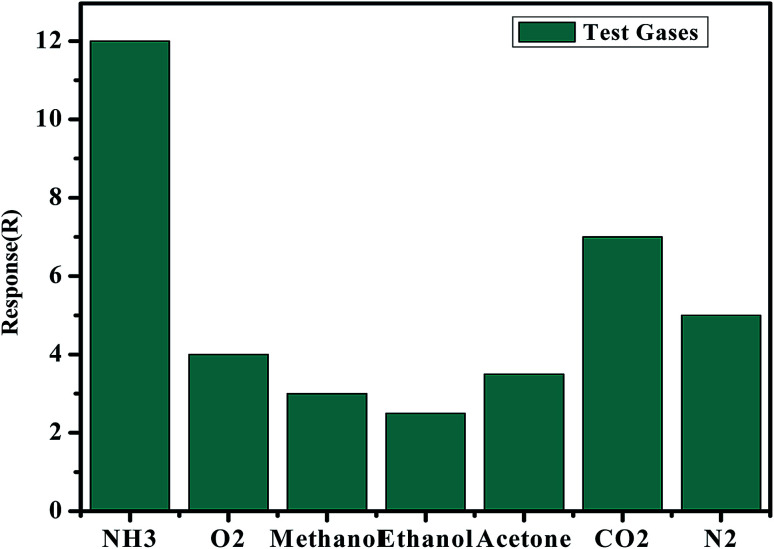
More quantitatively, a comparison of sensitivity evolution with the nature of the gas (Fig. 15) shows that NH3 provides a response that is at least 2.5 times larger than the other gases (methanol, ethanol, acetone, N2, CO2 and O2) of nearly equivalent sensitivity. The reaction of poly-GO (0.04 wt%) to the different gases can be ordered as follows from high to low response: NH3 > CO2 > N2 > O2 > acetone > methanol > ethanol. The selectivity and response results demonstrate that the response of the sensor depends not only on the chemical interactions between analytes and PTFE, PVDF, PANI chains, but also on such parameters as adsorption of analytes on the graphene oxide, accessibility to adsorption sites, and swelling at junctions between graphene foils.45
Fig. 15. Response of the sensor based on BiVO4–GO–PANI to various gases at 25 °C.
Conclusion
In conclusion, a series of poly-GO/BiVO4 heterojunction Schottky diodes were fabricated and their operation as room-temperature ammonia, N2 & O2 gas sensors was investigated. The highest sensitivity of the sensor was demonstrated for the poly-GO composite with 0.04 wt% loading of GO sheets in the presence of PANI polymer. The ammonia sensors were shown to have high sensitivity and fast response time to different NH3 concentrations. Poly-GO–BiVO4 films could be used as an active sensing material in Schottky diode-type sensing applications that require high speed, high sensitivity, and outstanding selectivity.
Conflicts of interest
There are no conflicts to declare.
Supplementary Material
References
- Aba L. Yusuf Y. Siswanta D. Triyana K. J. Nanotechnol. 2014;2014:864274. doi: 10.1155/2014/864274. [DOI] [Google Scholar]
- Chen H.-I. Hsiao C.-Y. Chen W.-C. Chang C.-H. Chou T.-C. Liu I.-P. Lin K.-W. Liu W.-C. Sens. Actuators, B. 2018;256:962. doi: 10.1016/j.snb.2017.10.032. [DOI] [Google Scholar]
- Ladhe R. Gurav K. Pawar S. Kim J. Sankapal B. J. Alloys Compd. 2012;515:80. doi: 10.1016/j.jallcom.2011.11.076. [DOI] [Google Scholar]
- Chen T.-Y. Chen H.-I. Liu Y.-J. Huang C.-C. Hsu C.-S. Chang C.-F. Liu W.-C. Sens. Actuators, B. 2011;155:347. doi: 10.1016/j.snb.2010.11.022. [DOI] [Google Scholar]
- Patil S. Deshmukh P. Lokhande C. Sens. Actuators, B. 2011;156:450. doi: 10.1016/j.snb.2011.04.005. [DOI] [Google Scholar]
- Salehi A. Nikfarjam A. Kalantari D. J. IEEE Sens. J. 2006;6:1415. [Google Scholar]
- Salehi A. Nikfarjam A. Kalantari D. J. Sens. Actuators, B. 2006;113:419. doi: 10.1016/j.snb.2005.03.064. [DOI] [Google Scholar]
- Late D. J. Huang Y. K. Liu B. Acharya J. Shirodkar S. N. Luo J. Yan A. Charles D. Waghmare U. V. Dravid V. P. Rao C. N. R. Sensing behavior of atomically thin-layered MoS2 transistors. ACS Nano. 2013;7(6):4879–4891. doi: 10.1021/nn400026u. [DOI] [PubMed] [Google Scholar]
- Kannan P. K. Late D. J. Morgan H. Rout C. S. Recent developments in 2D layered inorganic nanomaterials for sensing. Nanoscale. 2015;7(32):13293–13312. doi: 10.1039/C5NR03633J. [DOI] [PubMed] [Google Scholar]
- Late D. J. Doneux T. Bougouma M. Single-layer MoSe2 based NH3 gas sensor. Appl. Phys. Lett. 2014;105(23):233103. doi: 10.1063/1.4903358. [DOI] [Google Scholar]
- Erande M. B. Pawar M. S. Late D. J. Humidity sensing and photodetection behavior of electrochemically exfoliated atomically thin-layered black phosphorus nanosheets. ACS Appl. Mater. Interfaces. 2016;8(18):11548–11556. doi: 10.1021/acsami.5b10247. [DOI] [PubMed] [Google Scholar]
- Late D. J. Liquid exfoliation of black phosphorus nanosheets and its application as humidity sensor. Microporous Mesoporous Mater. 2016;225:494–503. doi: 10.1016/j.micromeso.2016.01.031. [DOI] [Google Scholar]
- Pawbake A. S. Waykar R. G. Late D. J. Jadkar S. R. Highly transparent wafer-scale synthesis of crystalline WS2 nanoparticle thin film for photodetector and humidity-sensing applications. ACS Appl. Mater. Interfaces. 2016;8(5):3359–3365. doi: 10.1021/acsami.5b11325. [DOI] [PubMed] [Google Scholar]
- Late D. J. Kanawade R. V. Kannan P. K. Rout C. S. Atomically thin WS2 nanosheets based gas sensor. Sens. Lett. 2016;14(12):1249–1254. doi: 10.1166/sl.2016.3764. [DOI] [Google Scholar]
- Gavgani J. N. Hasani A. Nouri M. Mahyari M. Salehi A. Sens. Actuators, B. 2016;229:239. doi: 10.1016/j.snb.2016.01.086. [DOI] [Google Scholar]
- Hasani A. Dehsari H. S. Gavgani J. N. Shalamzari E. K. Salehi A. Taromi F. A. Mahyari M. Microchim. Acta. 2015;182:1551. doi: 10.1007/s00604-015-1487-7. [DOI] [Google Scholar]
- Lin C.-Y. Chen J.-G. Hu C.-W. Tunney J. J. Ho K.-C. Sens. Actuators, B. 2009;140:402. doi: 10.1016/j.snb.2009.04.041. [DOI] [Google Scholar]
- Pawar M. Kadam S. Late D. J. High-performance sensing behavior using electronic ink of 2D SnSe2 nanosheets. ChemistrySelect. 2017;2(14):4068–4075. doi: 10.1002/slct.201700261. [DOI] [Google Scholar]
- Chitara B. Late D. J. Krupanidhi S. B. Rao C. N. R. Room-temperature gas sensors based on gallium nitride nanoparticles. Solid State Commun. 2010;150(41–42):2053–2056. doi: 10.1016/j.ssc.2010.08.007. [DOI] [Google Scholar]
- Dehsari H. S. Shalamzari E. K. Gavgani J. N. Taromi F. A. Ghanbary S. RSC Adv. 2014;4:55067. doi: 10.1039/C4RA09474C. [DOI] [Google Scholar]
- Lee C. Y. VanLe Q. Kim C. Kim S. Y. Phys. Chem. Chem. Phys. 2015;17:9369. doi: 10.1039/C5CP00507H. [DOI] [PubMed] [Google Scholar]
- Liu J. Xue Y. Gao Y. Yu D. Durstock M. Dai L. Adv. Mater. 2012;24:2228. doi: 10.1002/adma.201104945. [DOI] [PubMed] [Google Scholar]
- Sun Y. Tang J. Zhang K. Yuan J. Li J. Zhu D.-M. Ozawa K. Qin L.-C. Nanoscale. 2017;9:2585. doi: 10.1039/C6NR07650E. [DOI] [PubMed] [Google Scholar]
- Shah M. S. A. S. Muhammad S. Park J. H. Yoon W.-S. Yoo P. J. RSC Adv. 2015;5:13964. doi: 10.1039/C4RA15913F. [DOI] [Google Scholar]
- Ravula S. Zhang C. Essner J. B. Robertson J. D. Lin J. Baker G. A. ACS Appl. Mater. Interfaces. 2017;9:8065. doi: 10.1021/acsami.6b13578. [DOI] [PubMed] [Google Scholar]
- Xu J. Tan Z. Zeng W. Chen G. Wu S. Zhao Y. Ni K. Tao Z. Ikram M. Ji H. Adv. Mater. 2016;28:5222. doi: 10.1002/adma.201600586. [DOI] [PubMed] [Google Scholar]
- Choi Y. R. Yoon Y.-G. Choi K. S. Kang J. H. Shim Y.-S. Kim Y. H. Chang H. J. Lee J.-H. Park C. R. Kim S. Y. Carbon. 2015;91:178. doi: 10.1016/j.carbon.2015.04.082. [DOI] [Google Scholar]
- Wang T. Huang D. Yang Z. Xu S. He G. Li X. Hu N. Yin G. He D. Zhang L. Nano-Micro Lett. 2016;8:95. doi: 10.1007/s40820-015-0073-1. [DOI] [PMC free article] [PubMed] [Google Scholar]
- Huang D. Li X. Wang S. He G. Jiang W. Hu J. Wang Y. Hu N. Zhang Y. Yang Z. Sens. Actuators, B. 2017;252:956. doi: 10.1016/j.snb.2017.05.117. [DOI] [Google Scholar]
- Rella R. Siciliano P. Quaranta F. Primo T. Valli L. Schenetti L. Mucci A. Iarossi D. Sens. Actuators, B. 2000;68:203. doi: 10.1016/S0925-4005(00)00430-5. [DOI] [Google Scholar]
- Manera M. G. Ferreiro-Vila E. Cebollada A. García-Martín J. M. García-Martín A. Giancane G. Valli L. Rella R. J. Phys. Chem. C. 2012;116:10734. doi: 10.1021/jp3019843. [DOI] [Google Scholar]
- Rella R. Spadavecchia J. Ciccarella G. Siciliano P. Vasapollo G. Valli L. Sens. Actuators, B. 2003;89:86. doi: 10.1016/S0925-4005(02)00447-1. [DOI] [Google Scholar]
- Tanese M. C. Farinola G. M. Pignataro B. Valli L. Giotta L. Conoci S. Lang P. Colangiuli D. Babudri F. Naso F. Chem. Mater. 2006;18:778. doi: 10.1021/cm0524291. [DOI] [Google Scholar]
- Comini E. Anal. Chim. Acta. 2006;568:28. doi: 10.1016/j.aca.2005.10.069. [DOI] [PubMed] [Google Scholar]
- Gavgani J. N. Dehsari H. S. Hasani A. Mahyari M. Shalamzari E. K. Salehi A. Taromi F. A. RSC Adv. 2015;5:57559. doi: 10.1039/C5RA08158K. [DOI] [Google Scholar]
- Wu X. Liu J. Wu D. Zhao Y. Shi X. Wang J. Huang S. He G. J. Phys. Chem. C. 2014;2:4044. [Google Scholar]
- Wang C. Yin L. Zhang L. Xiang D. Gao R. Sensors. 2010;10:2088. doi: 10.3390/s100302088. [DOI] [PMC free article] [PubMed] [Google Scholar]
- Fine G. F. Cavanagh L. M. Afonja A. Binions R. Sensors. 2010;10:5469. doi: 10.3390/s100605469. [DOI] [PMC free article] [PubMed] [Google Scholar]
- Bai H. Shi G. Sensors. 2007;7:267. doi: 10.3390/s7030267. [DOI] [Google Scholar]
- Reemts J. Parisi J. Schlettwein D. Thin Solid Films. 2004;466:320. doi: 10.1016/j.tsf.2004.03.010. [DOI] [Google Scholar]
- Cho J.-H. Yu J.-B. Kim J.-S. Sohn S.-O. Lee D.-D. Huh J.-S. Sens. Actuators, B. 2005;108:389. doi: 10.1016/j.snb.2004.12.082. [DOI] [Google Scholar]
- Kemp N. Kaiser A. Trodahl H. Chapman B. Buckley R. Partridge A. Foot P. J. Polym. Sci., Part B: Polym. Phys. 2006;44:1331. doi: 10.1002/polb.20792. [DOI] [Google Scholar]
- Jian J. Guo X. Lin L. Cai Q. Cheng J. Li J. Sens. Actuators, B. 2013;178:279. doi: 10.1016/j.snb.2012.12.085. [DOI] [Google Scholar]


