Abstract
We demonstrate a highly efficient, single-step, cathodic exfoliation process of graphite to produce single- to few-layer graphene with a yield of over 70% from natural graphite flakes. By employing boron-doped diamond electrodes high potentials up to −60 V can be applied which was found to greatly increase the yield. The produced graphene flakes are partially hydrogenated during the electrochemical treatment likely aiding in their exfoliation. The resulting flakes have a large lateral size with up to 50 μm diameter. Due to the reversibility of the hydrogenation by thermal treatment the graphene flakes possess a low defect density as judged by the Raman D/G ratio yielding highly conductive films with sheet resistances of 100 to 3200 Ω □−1 at 10 to 70% transparency.
We demonstrate a highly efficient, single-step, cathodic exfoliation process of graphite to produce single- to few-layer graphene with a yield of over 70% from natural graphite flakes.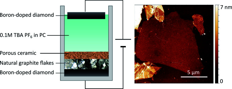
Introduction
Graphene, the two-dimensional form of sp2 hybridized carbon, has attracted tremendous interest from both research and industry due to its many outstanding properties.1 Graphene flakes, obtained by exfoliation of graphite, have shown great potential for applications like transparent, conductive films,2 electrodes for energy storage devices,3 or as conductive inks.4,5 While many methods for exfoliation have been reported,6–8 like the mechanical exfoliation via scotch tape,9 for the industrial application of graphene, however, a suitable production method is needed which delivers large amounts of graphene in good quality, i.e. high degree of exfoliation, large lateral flake size, and low defect density,10,11 since its quality determines the performance of the device.12 Liquid-phase exfoliation and the reduction of graphene oxide are able to produce large quantities of graphene. However, they require long sonication treatment and/or the use of toxic, environmentally harmful chemicals. Electrochemical routes on the other hand are more eco-friendly while also being scalable.13 Most reported successful electrochemical exfoliations occurred by anodic treatment.14–16 The resulting graphene, however, generally suffers from oxidation, which is known to result in irreversible damage.14 Averting oxidation is possible but requires the use of additives.17 Therefore, the cathodic exfoliation is a more promising approach. Inspired by the degradation of graphite in lithium-ion batteries containing propylene carbonate (PC) electrolytes, Wang et al.18 successfully exfoliated HOPG. Zhong and Swager19 increased the graphite expansion by adding the larger TBA cations. Other works have also used ammonium-based electrolytes for graphite exfoliation.20,21 Nevertheless, extensive sonication over hours is always needed to actually separate the graphene layers. Because even 30 min sonication greatly reduces the lateral graphene flake size,22 it is preferable to avoid sonication treatment. Another critical point is the type of graphite used for exfoliation since, especially in electrochemical exfoliation, the size of the resulting graphene is also determined by the crystal size of the graphite.14 The most commonly used HOPG is the easiest to exfoliate due to its high crystal orientation, but is very costly and thus not suitable for industrial production. Preformed graphites are more versatile for electrode design, but, while easier to exfoliate, the resulting graphene flakes are very small with submicrometer diameters.21 Furthermore, scalability may be limited.23 As Zhong et al.24 noted, the major limitation on the electrochemical route is the need to provide an unbroken voltage bias to the graphite. Since intercalation occurs not layer-by-layer but simultaneously, multi-layered graphite chunks are separated, lose electrical contact and will not be further exfoliated. Hence, there is a fundamental need to engineer a set up to allow continuous electrical contact.
Here we report successful exfoliation in a scalable reactor that allows the use of natural graphite flakes as starting material and overcomes the problem of premature material separation. By using boron-doped diamond (BDD) electrodes we are able to apply high negative potentials without degrading the electrode, leading to an overall graphene yield of more than 70% without any need for sonication treatments. The graphene flakes are partially hydrogenated due to the strong cathodic potentials as observed by infrared spectroscopic measurements. Contrary to oxidation, hydrogenation is reversible upon thermal annealing resulting in graphene flakes with a low defect-density.
Results and discussion
Electrochemical set up
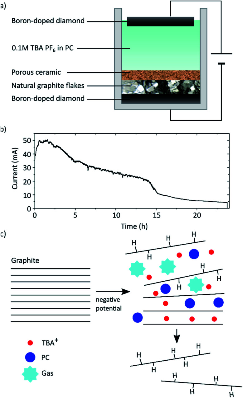
As shown in Fig. 1 natural graphite flakes were placed into a one-pot type reactor and pressed onto a BDD electrode with a porous membrane that allows diffusion of the electrolyte from and to the graphite flakes. This membrane was designed to enable movement during the electrochemical procedure to compensate for the volume expansion of the graphite. We found that if this movement was hindered, also the full exfoliation of the graphite was hampered. With this design natural graphite flakes can be used as starting material instead of uneconomical HOPG or graphite foils and rods that possess a far smaller lateral crystal structure.21 Employing BDD as electrodes allows the application of high potentials up to −60 V. As far as we know, graphite exfoliation under such high potentials has never been investigated before. In so far published reports, Pt is commonly used as electrode. However, Pt is not completely resistant and dissolves, especially under anodic conditions.25 This may lead to impurities in the graphene flakes and makes the expensive electrode a wearing part. BDD on the other hand is known for its exceptional stability even when applying high potentials,26 is readily available at large scale through, e.g., chemical vapour deposition,27 and is easily reconditioned. Tetrabutylammonium hexafluorophosphate (TBA PF6) solved in PC was used as electrolyte. PC has a surface tension of 40 mJ m−2 (ref. 28) which is close to that of graphite (around 55 mJ m−2 (ref. 29)) and thus ideal to solvate the exfoliated graphene layers and hinder reaggregation.14 Furthermore, PC presents a more environmentally-friendly alternative to commonly used non-aqueous solvents like DMF or NMP. It was also shown that PC does not form a solid electrolyte interphase layer, which would protect the graphite layers from exfoliation.30–32
Fig. 1. (a) Schematic of the reactor used to exfoliate natural graphite flakes. (b) Current response during the exfoliation at −60 V applied across the reactor, i.e. between the two diamond electrodes. (c) Schematic of the exfoliation process.
The graphite was exfoliated by applying a constant potential of −60 V across the cell for 24 h.
Exfoliation of the graphite is assumed to occur due to two main processes as depicted schematically in Fig. 1c. First the TBA+ from the electrolyte intercalates between the graphite layers. TBA as cation was chosen, since it has been demonstrated to intercalate graphite and form graphite intercalation compounds (GICs).31,33 Cyclic voltammetry (CV) was carried out to confirm the intercalation (see ESI Fig. S9†). Advantageously to Li, TBA is sterically larger thus leading to an increased expansion of the graphite layers. Due to this, co-intercalation of the PC becomes possible.18,31 Once intercalated the PC decomposes due to the applied high negative potential forming propene and carbonate gas.34,35 The corresponding CV is also depicted in the ESI.† The graphite expansion and partial exfoliation due to this solvent co-intercalation and subsequent decomposition has been studied before.21,31,36 This observed gas evolution can cause a tremendous pressure that overcomes the van der Waals attraction between the graphite layers and forces exfoliation of the sheets.37
We found that increasing the applied voltage from −30 V to −60 V we could increase the graphene yield dramatically from 10% to over 70% (plot shown in ESI Fig. S7†). We assume that higher potentials lead to accelerated reaction rates and more violent gas evolution facilitating the separation. In the commonly reported set ups with single bulk graphite electrodes this leads to premature separation of chunks that then loose electrical contact and are not further exfoliated.38 Whereas in our design those chunks remain in contact and can be further exfoliated. At the lower potential of −30 V we observed mostly GIC formation without full exfoliation indicating that the vigorous gas evolution by electrolyte decomposition may play a crucial role in exfoliation. Another factor may be the onset of graphene hydrogenation, which will be discussed below.
The current response at an applied voltage of −60 V is shown in Fig. 1b. In the first stages the recorded current drastically increases reaching a steady state after approximately 1 h. This increase is associated with capacitive charging and the intercalation process of the TBA ions. The intercalation results in an increase of the cathode surface area, i.e. the graphite on BDD, which in turn leads to self-enhancing of both processes due to more easily accessible surface area and the dependence of current on electrode area.39 Additionally the decomposition of PC will lead to a background current depending on the available electrode area and the cell potential (i.e. the applied potential compensated for the IR-drop). Eventually the current decreases due to an increasing resistance of the cathode caused by the continuously occurring hydrogenation and separation of graphene flakes as well as the likely presence of trapped gas.
Characterisation of the produced graphene flakes
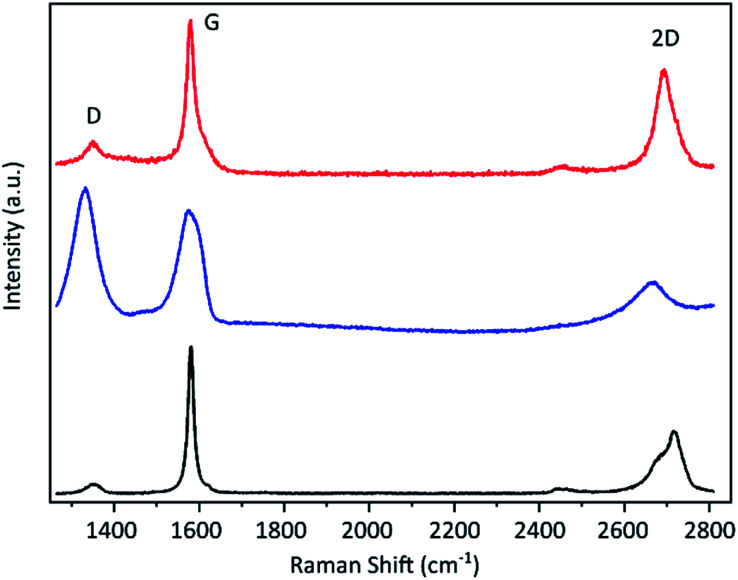
The resulting graphene flakes were first characterised via Raman spectroscopy. The representative spectra before and after the electrochemical treatment are shown in Fig. 2. The starting material graphite shows three significant peaks.40 The G band around 1590 cm−1 arises due to in-plane vibrations of sp2 hybridized carbon atoms and is a doubly degenerate phonon mode at the Brillouin zone centre. The D band around 1350 cm−1 originates from the breathing modes of the six-atom rings of the graphene lattice and requires a defect for its activation. The D/G band ratio is, therefore, a qualitative indicator for the material's defect density.41 The graphite flakes show a very small D band indicating a low defect density in the starting material. The 2D band at around 2680 cm−1 arises due to a two phonon intervalley double resonance scattering near the boundary of the Brillouin zone and is closely linked to the electronic band structure.40 This band becomes asymmetric for more than 10 layers as is the case for the graphite flakes. After the electrochemical process the D band strongly increases indicating the introduction of a large number of sp3 defects by our method. This also causes the 2D band to broaden and flatten. In addition a new peak emerges at around 2900 cm−1 (shown in ESI†), which is the combination of D + D′. We propose that this transformation is caused by a hydrogenation of the graphene lattice during the electrochemical reduction under the applied high cathodic potential. Hydrogenated graphene produced by Birch reduction of graphite42 as well as by plasma treatment hydrogenated graphene43,44 show remarkably similar spectra. As possible source for the hydrogen we propose the used TBA ion. It was shown that it can act as proton donor in aprotic solvents like PC45 and the hydrogenation of graphene by electrochemical reduction with ammonium ion containing electrolytes was previously demonstrated.46,47
Fig. 2. Raman spectra of the graphite flakes (black line), the material after electrochemical exfoliation (blue) and after subsequent thermal treatment above 600 °C (red).
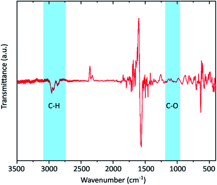
To confirm the presence of hydrogen IR spectroscopy was carried out (Fig. 3). Neither C–O (around 1050 cm−1) nor C O (1700–1750 cm−1) vibrational bands are visible proving that the defects are not induced by oxidation. Instead, distinctive peaks in the range of 2800 to 2900 cm−1 are visible which indicates the formation of C–H bonds. Similar features have also been reported by other hydrogenated graphenes.42,47
Fig. 3. FTIR spectrum of the graphene flakes. The silicon substrate signal was used for baseline correction giving rise to the peaks in the range below 1700 cm−1. The uncorrected spectra for both substrate and the graphene sample are shown in the ESI.† The shaded areas mark the presence of C–H vibrations and the absence of C–O bands.
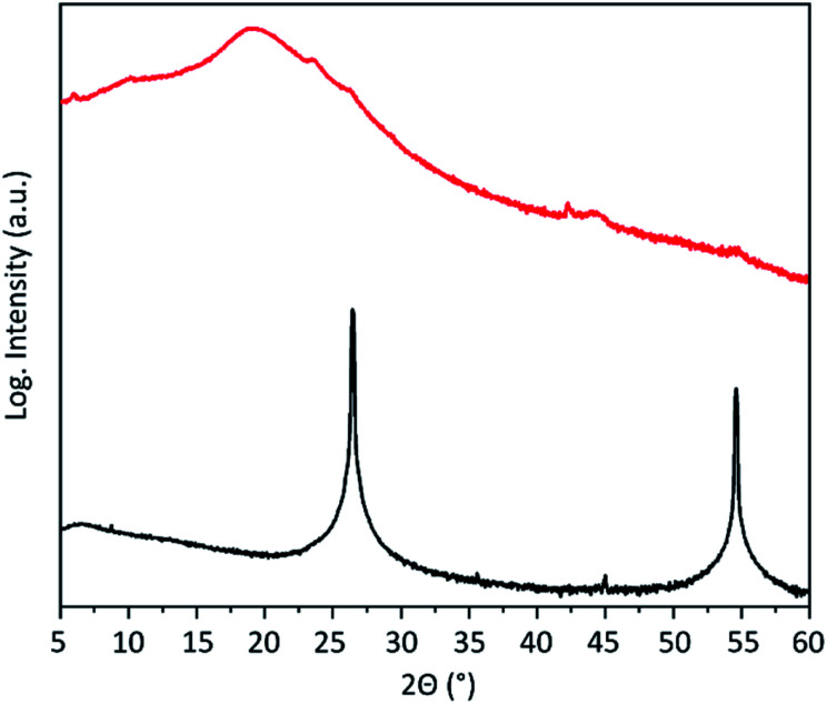
The expansion and exfoliation of the graphite has been further investigated by X-ray diffraction (XRD). Graphite shows two prominent reflections (Fig. 4). One is at 2θ = 26.3° corresponding to the (002) crystal planes of graphite with an inter-layer distance of 3.35 Å and one at 54.4° corresponding to the (004) crystal planes. After electrochemical exfoliation those reflections almost disappear. This indicates the loss of stacking order along the c-axis and confirms successful expansion of the majority of graphite. Instead, a broad peak appears at around 19.2° corresponding to an inter-layer distance of the graphene layers of around 4.6 Å. This is in accordance with the calculated48 and experimentally found42 inter-layer distance of hydrogenated graphene.
Fig. 4. XRD pattern of the graphite flakes before (black) and after (red) electrochemical exfoliation.
Hydrogenation of the graphene as cause for the observed induced defects as indicated by the Raman D peak is further supported by the fact that the D peak decreases upon thermal annealing (Fig. 2), since it is known that hydrogenation is reversible by annealing.43,44 After annealing at over 600 °C the Raman D peak is significantly reduced and a low D/G ratio can be achieved. Statistical analysis of the annealed material reveals an average D/G ratio of around 0.15 with the majority being below 0.2. The histogram is depicted in the ESI.† The remaining defects may be caused by stress due to deformation during hydrogenation and intercalation or slight damage caused by the evolving gas during the electrochemical reduction of the electrolyte. Nevertheless, the D/G ratio afterwards is only slightly higher than that of the starting material (which has an average of 0.1), which means that our method induces only few defects. A Raman mapping of graphene flakes and the D/G ratio before and after annealing is shown in the ESI Fig. S8.†
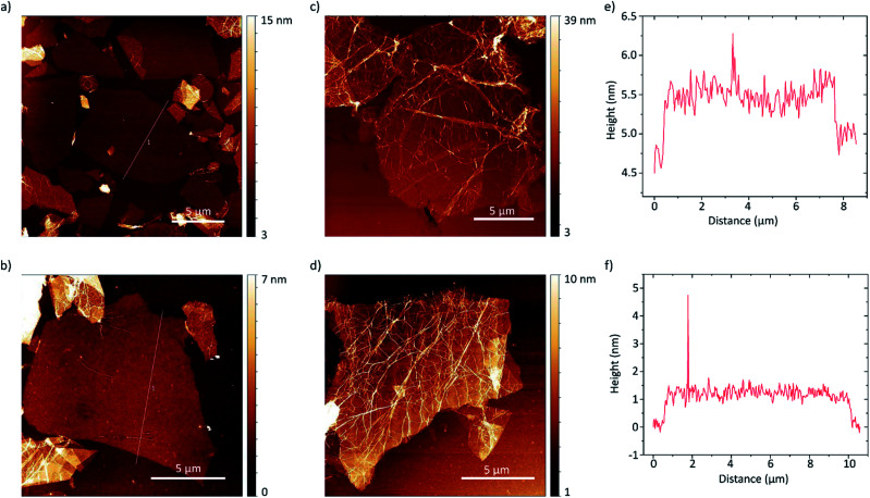
The thickness of the exfoliated flakes was investigated by atomic force microscopy (AFM) as depicted in Fig. 5. The flakes show heights from around 0.8 nm to 2.5 nm. Taking the presence of a hydration layer between the SiO2 substrate and graphene with a thickness around 1 nm (ref. 9) into account, the flakes with thicknesses around 0.8 nm can be identified as single-layer graphene.49 We found that they also show a flat morphology and thus likely better adherence to the substrate. Considering the inter-layer distance of hydrogenated graphene of 0.46 nm a height of 2.5 nm likely corresponds to four-layer graphene. Oftentimes though, the flakes are wrinkled, likely due to stress induced by hydrogenation, as can be seen in Fig. 5c and d. The wrinkled morphology is more pronounced in multi-layer graphene flakes. This makes accurate determination of the layer number difficult. Furthermore, the flakes tend to agglomerate.
Fig. 5. (a–d) AFM height images of hydrogenated graphene flakes on SiO2 (300 nm)/Si substrates. The profile lines shown in (a) and (b) are depicted in (e) and (f) respectively.
Therefore, to get a statistically more relevant information of the whole material, we analysed the shape of the Raman 2D band as described elsewhere50 since this method is independent of agglomeration and sample preparation. The Raman 2D band shows a clear distinction between graphene (few-layer graphene) and graphite in its symmetry or asymmetry, respectively, and can be used to discern the two. From this evaluation of over 800 spectra we find that over 70% of the investigated material consists of few-layer graphene. Having extracted the whole material after electrochemical treatment, we can draw conclusions to the yield of our process. Therefore, we determine the exfoliation efficiency of our method to yield more than 70% graphene. Since the hydrogenation affects the shape of the 2D band,42 we determined the yield after annealing. Thermal annealing may assist in further exfoliation of flakes where intercalation and/or hydrogenation was insufficient to lead to full exfoliation, but it may also lead to re-graphitization of the flakes and thus influence the measured yield in either direction.51 Observations of flakes before and after annealing indicate that sufficiently hydrogenated flakes with a D/G ratio above 0.5 show a symmetric 2D band after dehydrogenation. Assuming this to be the case the majority of times we also estimated the yield by a D/G ratio over 0.5 to be around 80%. This value approximately matches the yield after annealing.
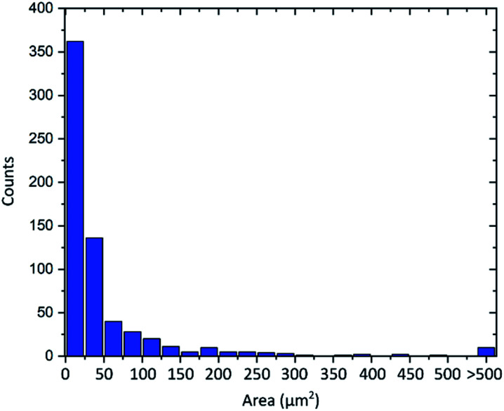
Another important property of graphene flakes is the lateral size.10,11 As is always the case for graphene obtained by graphite exfoliation,52 the material consists of flakes with various diameters. As visible in the AFM images the flakes show diameters from around 2 μm to 15 μm. An evaluation of more than 600 flakes from optical microscope images is shown in Fig. 6. The flakes' area follows an asymmetric distribution with an average flake area of 55 μm2. Flake sizes up to 2000 μm2 can be observed, which corresponds to a diameter of about 50 μm.
Fig. 6. Distribution of the graphene flakes' area of more than 600 flakes.
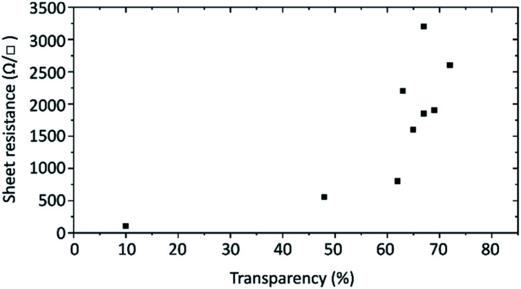
Finally, the electrical conductivity of the prepared graphene flakes was investigated. For this transparent films were prepared by Langmuir–Blodgett technique onto 2 × 2 cm2 quartz glass substrates and annealed at over 600 °C to remove the graphene flakes' hydrogenation. The electrical resistance was measured by the van der Pauw method. The sheet resistance of films with different transparencies is plotted in Fig. 7. For films with around 70% transmittance at 550 nm the sheet resistance ranges from about 1.6k to 3.2k Ω □−1. The variation is caused by how well the flakes overlap in the film. With less transparent films the sheet resistance decreases, dropping to 550 Ω □−1 at 48% transparency and as low as 105 Ω □−1 at 10%.
Fig. 7. Sheet resistances of the produced 2 × 2 cm2 graphene films in relation to the transparency at 550 nm.
Conclusions
We introduced an electrochemical one-pot reactor that enables the use of natural graphite flakes and their exfoliation under high cathodic potentials by employing BDD electrodes. With that the production of graphene flakes with an efficiency of over 70% could be achieved. During this process we found a hydrogenation of the graphene flakes to occur, which may aid in the exfoliation of graphite. The resulting graphene flakes are of high quality, consisting of predominantly few-layer graphene, possessing large flake areas with on average 55 μm2 and up to 2000 μm2, and a low defect density due to the reversibility of the occurring hydrogenation. Transparent films could be prepared with sheet resistances from 100 to 3200 Ω □−1.
Experimental
Materials and electrochemical set up
The natural graphite flakes (Schunk Hoffmann Carbon Technologies AG, Austria) were exfoliated in a two-electrode electrochemical reactor. The graphite flakes were pressed onto the cathode with a permeable ceramic. For both cathode and anode boron-doped diamond (BDD) was used. For the cathode, prime grade 4′′ silicon wafers with a resistivity in the range of 0.01–0.02 Ω cm (p-type, Si-Mat, Germany) were overgrown with BDD. Prior to growth, nanodiamond seeding was carried out using 4 nm hydrogen-terminated nanodiamonds (G01 grade, Plasmachem GmbH, Germany) following a procedure described elsewhere.53 Diamond growth was carried out in an ellipsoidal MPCVD reactor using purified gases (hydrogen, methane, and trimethylborane).54 The following growth conditions were used: 9 kW microwave power, 750 °C substrate temperature, 50 mbar pressure, a methane concentration of 2% in H2, and a B/C ratio of 2000 ppm. After 30 h process duration, an approximately 5 μm thick BDD film was obtained with a dopant concentration of more than 1021 B/cm3 (determined by secondary ion mass spectrometry). As anode, a polycrystalline diamond wafer was overgrown with BDD on both sides using the same conditions. The electrolyte was prepared by solving 0.1 M tetrabutylammonium hexafluorophosphate (Sigma Aldrich) in propylene carbonate (anhydrous, Sigma Aldrich). The voltage was applied via a Keithley 2614B.
Sample preparation
Graphene flake dispersions were achieved by washing of the flakes with acetone and isopropanol over filter paper and then dispersed in isopropanol by brief sonication in an ultrasonic bath (Bandelin Sonorex, 35 kHz). Then the flakes were dip-coated onto silicon substrates with a 300 nm oxide layer for Raman spectroscopy, AFM and optical microscope characterisation, and onto silicon for FTIR analysis. For XRD analysis the material was collected after washing and pasted onto a zero-background silicon holder. The transparent films were obtained by Langmuir–Blodgett technique where the graphene flakes assembled on a water surface, were transferred onto quartz glass substrate and subsequently annealed for dehydrogenation. The dehydrogenation was carried out by annealing at over 600 °C under vacuum in a tube furnace.
Characterisation techniques
Atomic force microscopy (AFM) measurements were performed under ambient conditions using a NanoWizard 3 System (NanoWizard 3, JPK Instruments) in tapping mode with a PPP-NCHR AFM probe. Raman spectra were obtained with an InVia Raman microscope with a 532 nm excitation laser, 1800 mm−1 grating and a spatial resolution of 1 mm from Renishaw, Gloucestershire, UK. Fourier-transform infrared spectroscopy (FTIR) was performed at room temperature with a Bruker Invenio R spectrometer. X-ray diffraction (XRD) measurements were carried out on a Panalytical Empyrean 2 diffractometer with a Ge 220 monochromator, CuKα1 radiation (λ = 0.154056 nm) and a programmable anti-scatter slit.
Conflicts of interest
There are no conflicts to declare.
Supplementary Material
Acknowledgments
The authors wish to thank Klaus Schwarz for the FTIR measurements.
Electronic supplementary information (ESI) available. See DOI: 10.1039/c9ra04795f
References
- Novoselov K. S. Fal'ko V. I. Colombo L. Gellert P. R. Schwab M. G. Kim K. Nature. 2012;490:192–200. doi: 10.1038/nature11458. [DOI] [PubMed] [Google Scholar]
- Bonaccorso F. Sun Z. Hasan T. Ferrari A. C. Nat. Photonics. 2010;4:611–622. doi: 10.1038/nphoton.2010.186. [DOI] [Google Scholar]
- Ke Q. Wang J. J. Materiomics. 2016;2:37–54. doi: 10.1016/j.jmat.2016.01.001. [DOI] [Google Scholar]
- Torrisi F. Hasan T. Wu W. Sun Z. Lombardo A. Kulmala T. S. Hsieh G.-W. Jung S. Bonaccorso F. Paul P. J. Chu D. Ferrari A. C. ACS Nano. 2012;6:2992–3006. doi: 10.1021/nn2044609. [DOI] [PubMed] [Google Scholar]
- Qiang S. Carey T. Arbab A. Song W. Wang C. Torrisi F. Nanoscale. 2019;11:9912–9919. doi: 10.1039/C9NR00463G. [DOI] [PubMed] [Google Scholar]
- Zheng J. Di C.-a. Liu H. Guo Y. Du C. Wu T. Yu G. Zhu D. Chem. Commun. 2010;46:5728–5730. doi: 10.1039/C0CC00954G. [DOI] [PubMed] [Google Scholar]
- Shih C.-J. Vijayaraghavan A. Krishnan R. Sharma R. Han J.-H. Ham M.-H. Jin Z. Lin S. Paulus G. L. C. Reuel N. F. Wang Q. H. Blankschtein D. Strano M. S. Nat. Nanotechnol. 2011;6:439–445. doi: 10.1038/nnano.2011.94. [DOI] [PubMed] [Google Scholar]
- Li J.-M. Fang J. J. Mater. Chem. C. 2017;5:9545–9551. doi: 10.1039/C7TC03736H. [DOI] [Google Scholar]
- Novoselov K. S. Geim A. K. Morozov S. V. Jiang D. Zhang Y. Dubonos S. V. Grigorieva I. V. Firsov A. A. Science. 2004;306:666–669. doi: 10.1126/science.1102896. [DOI] [PubMed] [Google Scholar]
- Kauling A. P. Seefeldt A. T. Pisoni D. P. Pradeep R. C. Bentini R. Oliveira R. V. B. Novoselov K. S. Castro Neto A. H. Adv. Mater. 2018;30:1803784. doi: 10.1002/adma.201803784. [DOI] [PubMed] [Google Scholar]
- Kovtun A. Treossi E. Mirotta N. Scidà A. Liscio A. Christian M. Valorosi F. Boschi A. Young R. J. Galiotis C. Kinloch I. A. Morandi V. Palermo V. 2D Mater. 2019;6:25006. doi: 10.1088/2053-1583/aafc6e. [DOI] [Google Scholar]
- Raccichini R. Varzi A. Passerini S. Scrosati B. Nat. Mater. 2015;14:271–279. doi: 10.1038/nmat4170. [DOI] [PubMed] [Google Scholar]
- Yang S. Lohe M. R. Müllen K. Feng X. Adv. Mater. 2016;28:6213–6221. doi: 10.1002/adma.201505326. [DOI] [PubMed] [Google Scholar]
- Abdelkader A. M. Cooper A. J. Dryfe R. A. W. Kinloch I. A. Nanoscale. 2015;7:6944–6956. doi: 10.1039/C4NR06942K. [DOI] [PubMed] [Google Scholar]
- Cao J. He P. Mohammed M. A. Zhao X. Young R. J. Derby B. Kinloch I. A. Dryfe R. A. W. J. Am. Chem. Soc. 2017;139:17446–17456. doi: 10.1021/jacs.7b08515. [DOI] [PubMed] [Google Scholar]
- Parvez K. Wu Z.-S. Li R. Liu X. Graf R. Feng X. Müllen K. J. Am. Chem. Soc. 2014;136:6083–6091. doi: 10.1021/ja5017156. [DOI] [PubMed] [Google Scholar]
- Yang S. Brüller S. Wu Z.-S. Liu Z. Parvez K. Dong R. Richard F. Samorì P. Feng X. Müllen K. J. Am. Chem. Soc. 2015;137:13927–13932. doi: 10.1021/jacs.5b09000. [DOI] [PubMed] [Google Scholar]
- Wang J. Manga K. K. Bao Q. Loh K. P. J. Am. Chem. Soc. 2011;133:8888–8891. doi: 10.1021/ja203725d. [DOI] [PubMed] [Google Scholar]
- Zhong Y. L. Swager T. M. J. Am. Chem. Soc. 2012;134:17896–17899. doi: 10.1021/ja309023f. [DOI] [PubMed] [Google Scholar]
- Yang Y. Ji X. Yang X. Wang C. Song W. Chen Q. Banks C. E. RSC Adv. 2013;3:16130. doi: 10.1039/C3RA43010C. [DOI] [Google Scholar]
- Cooper A. J. Wilson N. R. Kinloch I. A. Dryfe R. A. Carbon. 2014;66:340–350. doi: 10.1016/j.carbon.2013.09.009. [DOI] [Google Scholar]
- Liscio A. Kouroupis-Agalou K. Betriu X. D. Kovtun A. Treossi E. Pugno N. M. de Luca G. Giorgini L. Palermo V. 2D Mater. 2017;4:25017. doi: 10.1088/2053-1583/aa57ff. [DOI] [Google Scholar]
- Yu P. Tian Z. Lowe S. E. Song J. Ma Z. Wang X. Han Z. J. Bao Q. Simon G. P. Li D. Zhong Y. L. Chem. Mater. 2016;28:8429–8438. doi: 10.1021/acs.chemmater.6b04415. [DOI] [Google Scholar]
- Zhong Y. L. Tian Z. Simon G. P. Li D. Mater. Today. 2015;18:73–78. doi: 10.1016/j.mattod.2014.08.019. [DOI] [Google Scholar]
- Jovanovič P. Šelih V. S. Šala M. Hodnik N. npj Mater. Degrad. 2018;2:1533. [Google Scholar]
- Hoffmann R. Kriele A. Obloh H. Hees J. Wolfer M. Smirnov W. Yang N. Nebel C. E. Appl. Phys. Lett. 2010;97:52103. doi: 10.1063/1.3476346. [DOI] [Google Scholar]
- Nishimura K. Das K. Glass J. T. J. Appl. Phys. 1991;69:3142–3148. doi: 10.1063/1.348582. [DOI] [Google Scholar]
- Adamson W. and Gast A. P., Physical Chemistry of Surfaces, Wiley-Interscience, 6th edn, 1997 [Google Scholar]
- Wang S. Zhang Y. Abidi N. Cabrales L. Langmuir. 2009;25:11078–11081. doi: 10.1021/la901402f. [DOI] [PubMed] [Google Scholar]
- Wagner M. R. Albering J. H. Moeller K.-C. Besenhard J. O. Winter M. Electrochem. Commun. 2005;7:947–952. doi: 10.1016/j.elecom.2005.06.009. [DOI] [Google Scholar]
- Chung G.-C. Kim H.-J. Yu S.-I. Jun S.-H. Choi J.-w. Kim M.-H. J. Electrochem. Soc. 2000;147:4391–4398. doi: 10.1149/1.1394076. [DOI] [Google Scholar]
- Xu K. Chem. Rev. 2004;104:4303–4418. doi: 10.1021/cr030203g. [DOI] [PubMed] [Google Scholar]
- Sirisaksoontorn W. Adenuga A. A. Remcho V. T. Lerner M. M. J. Am. Chem. Soc. 2011;133:12436–12438. doi: 10.1021/ja2053539. [DOI] [PubMed] [Google Scholar]
- Dey A. N. Sullivan B. P. J. Electrochem. Soc. 1970;117:222–224. doi: 10.1149/1.2407470. [DOI] [Google Scholar]
- Eichinger G. J. Electroanal. Chem. 1976;74:183–193. doi: 10.1016/S0022-0728(76)80234-3. [DOI] [Google Scholar]
- Cooper A. J. Velický M. Kinloch I. A. Dryfe R. A. J. Electroanal. Chem. 2014;730:34–40. doi: 10.1016/j.jelechem.2014.07.025. [DOI] [Google Scholar]
- Xia Z. Y. Pezzini S. Treossi E. Giambastiani G. Corticelli F. Morandi V. Zanelli A. Bellani V. Palermo V. Adv. Funct. Mater. 2013;69:4684–4693. [Google Scholar]
- Yang C.-Y. Wu C.-L. Lin Y.-H. Tsai L.-H. Chi Y.-C. Chang J.-H. Wu C.-I. Tsai H.-K. Tsai D.-P. Lin G.-R. Opt. Mater. Express. 2013;3:1893. doi: 10.1364/OME.3.001893. [DOI] [Google Scholar]
- Bard A. J. and Faulkner L. R., Electrochemical Methods. Fundamentals and Applications, John Wiley & Sons, New York, 2nd edn, 2001 [Google Scholar]
- Ferrari A. C. Meyer J. C. Scardaci V. Casiraghi C. Lazzeri M. Mauri F. Piscanec S. Jiang D. Novoselov K. S. Roth S. Geim A. K. Phys. Rev. Lett. 2006;97:187401. doi: 10.1103/PhysRevLett.97.187401. [DOI] [PubMed] [Google Scholar]
- Ferrari A. C. Basko D. M. Nat. Nanotechnol. 2013;8:235–246. doi: 10.1038/nnano.2013.46. [DOI] [PubMed] [Google Scholar]
- Yang Z. Sun Y. Alemany L. B. Narayanan T. N. Billups W. E. J. Am. Chem. Soc. 2012;134:18689–18694. doi: 10.1021/ja3073116. [DOI] [PubMed] [Google Scholar]
- Elias D. C. Nair R. R. Mohiuddin T. M. G. Morozov S. V. Blake P. Halsall M. P. Ferrari A. C. Boukhvalov D. W. Katayama M. Geim A. K. Novoselov K. S. Science. 2009;323:610–613. doi: 10.1126/science.1167130. [DOI] [PubMed] [Google Scholar]
- Luo Z. Yu T. Kim K.-J. Ni Z. You Y. Lim S. Shen Z. Wang S. Lin J. ACS Nano. 2009;3:1781–1788. doi: 10.1021/nn900371t. [DOI] [PubMed] [Google Scholar]
- Dahm C. E. Peters D. G. J. Electroanal. Chem. 1996;402:91–96. doi: 10.1016/0022-0728(95)04209-1. [DOI] [Google Scholar]
- Zhao M. Guo X.-Y. Ambacher O. Nebel C. E. Hoffmann R. Carbon. 2015;83:128–135. doi: 10.1016/j.carbon.2014.11.033. [DOI] [Google Scholar]
- Abdelkader A. M. Patten H. V. Li Z. Chen Y. Kinloch I. A. Nanoscale. 2015;7:11386–11392. doi: 10.1039/C5NR02840J. [DOI] [PubMed] [Google Scholar]
- Rohrer J. Hyldgaard P. Phys. Rev. B: Condens. Matter Mater. Phys. 2011;83:165423. doi: 10.1103/PhysRevB.83.165423. [DOI] [Google Scholar]
- Shearer C. J. Slattery A. D. Stapleton A. J. Shapter J. G. Gibson C. T. Nanotechnology. 2016;27:125704. doi: 10.1088/0957-4484/27/12/125704. [DOI] [PubMed] [Google Scholar]
- Roscher S. Hoffmann R. Ambacher O. Anal. Methods. 2019;11:1224–1228. doi: 10.1039/C8AY02619J. [DOI] [Google Scholar]
- Shih C.-J. Vijayaraghavan A. Krishnan R. Sharma R. Han J.-H. Ham M.-H. Jin Z. Lin S. Paulus G. L. C. Reuel N. F. Wang Q. H. Blankschtein D. Strano M. S. Nat. Nanotechnol. 2011;6:439–445. doi: 10.1038/nnano.2011.94. [DOI] [PubMed] [Google Scholar]
- Palermo V. Kinloch I. A. Ligi S. Pugno N. M. Adv. Mater. 2016;28:6232–6238. doi: 10.1002/adma.201505469. [DOI] [PubMed] [Google Scholar]
- Yoshikawa T. Zuerbig V. Gao F. Hoffmann R. Nebel C. E. Ambacher O. Lebedev V. Langmuir. 2015;31:5319–5325. doi: 10.1021/acs.langmuir.5b01060. [DOI] [PubMed] [Google Scholar]
- Füner M. Wild C. Koidl P. Appl. Phys. Lett. 1998;72:1149–1151. doi: 10.1063/1.120997. [DOI] [Google Scholar]
Associated Data
This section collects any data citations, data availability statements, or supplementary materials included in this article.


