Abstract
This paper presents a dual-frequency piezoelectric micromachined ultrasonic transducer (pMUT) array based on thin ceramic PZT for endoscopic photoacoustic imaging (PAI) applications. With a chip size of 7 × 7 mm2, the pMUT array consists of 256 elements, half of which have a lower resonant frequency of 1.2 MHz and the other half have a higher resonant frequency of 3.4 MHz. Ceramic PZT, with outstanding piezoelectric coefficients, has been successfully thinned down to a thickness of only 4 μ by using wafer bonding and chemical mechanical polishing (CMP) techniques and employed as the piezoelectric layer of the pMUT elements. The diaphragm diameters of the lower-frequency and higher-frequency elements are 220 μm and 120 μm, respectively. The design methodology, multiphysics modeling, fabrication process, and characterization of the pMUTs are presented in detail. The fabricated pMUT array has been fully characterized via electrical, mechanical, and acoustic measurements. The measured maximum responsivities of the lower- and higher- frequency elements reach 110 nm/V and 30 nm/V at their respective resonances. The measured cross-couplings of the lower-frequency elements and higher-frequency elements are about 9% and 5%, respectively. Furthermore, PAI experiments with pencil leads embedded into an agar phantom have been conducted, which clearly shows the advantages of using dual-frequency pMUT arrays to provide comprehensive photoacoustic images with high spatial resolution and large signal-to-noise ratio simultaneously.
Keywords: Microelectromechanical systems (MEMS), piezoelectric micromachined ultrasonic transducers (pMUTs), pMUT arrays, dual-frequency, ceramic PZT, photoacoustic imaging (PAI), endoscopic imaging
I. Introduction
PHOTOACOUSTIC imaging (PAI), an emerging imaging technology, has been developed based on the photoacoustic effect and evolved rapidly in the last decade with a wide range of applications in preclinical or clinical phases, such as cancer detection [1], brain imaging [2], hemodynamic study [3], and arthritis diagnosis [4]. In PAI, short laser pulses (usually in nanoseconds) are used to illuminate tissue samples, which will absorb the optical energy and generate photoacoustic pulses in ultrasonic frequencies due to the temperature rise and thermal elastic expansion. The laser induced photoacoustic signals will propagate and be detected by a single element ultrasonic transducer (UT) or an array of UTs. By acoustically detecting the optical absorption contrast, PAI offers several advantages over current biomedical imaging techniques. Firstly, it uses nonionizing radiation and is more compact and less expensive than X-ray computed tomography (CT), magnetic resonance imaging (MRI), and positron emission computed tomography (PET) [5]. Secondly, it can provide much larger imaging depth than pure optical imaging techniques, such as optical coherent tomography (OCT) and fluorescence microscopy, since the acoustic scattering is two to three orders of magnitude lower than the optical scattering in tissues [6]. Thirdly, it can provide functional imaging with physiological parameters revealed, such as oxygen saturation and hemoglobin concentration [7].
With the advantages described above, PAI has been extensively exploited to image microvasculatures, tumors, brains, human extremities, and small animals with high resolution and large imaging depth based on bench-top systems [8]. However, the typical imaging depth of PAI is still limited to less than 5 cm by the strong attenuation of the excitation laser in human tissues. This means that PAI must be incorporated into endoscopic imaging systems so that it can be used to diagnose internal organs inside human body. Endoscopic PAI has been actively explored through the past decade [9], but its clinical application is still at an early stage. One of the key challenges is the miniaturization of the imaging components while maintaining their high performance.
A single-element UT or an UT array is the key component in a PAI system, as its acoustic center frequency, bandwidth, and sensitivity will largely determine the spatial resolution and the imaging depth of the PAI system. Higher-frequency UTs can achieve higher spatial resolutions, but will result in lower signal-to-noise ratios (SNRs) and smaller imaging depths due to the increased acoustic attenuation [10]. Therefore, multifrequency UTs or UT arrays are demanded for endoscopic PAI to achieve both high spatial resolution and large imaging depth simultaneously.
Conventional UTs are bulky and work on the thickness extension mode of piezoelectric plates with their thicknesses designed as half of the acoustic wavelengths. Therefore, it is expensive and challenging to make them with multiple working frequencies. By contrast, micromachined ultrasonic transducers (MUTs) with advantages of very small footprint, scalable fabrication at low cost, and easy integration with electronics have drawn increasing attention for endoscopic PAI applications [11]. Two types of MUTs, capacitive MUTs (cMUTs) and piezoelectric MUTs (pMUTs), have been developed and applied for PAI [12]–[15]. For example, by incorporating cMUT membranes with different sizes into one chip, multifrequency cMUT arrays have been developed for PAI [16], [17]. However, cMUTs require high polarization voltages and very small capacitive gaps for high sensitivity, which impose challenges for biomedical applications and fabrication processes. The small capacitances also make them vulnerable to parasitic effects. By contrast, pMUTs, with advantages of more design flexibility and easy fabrication, have been extensively studied with different piezoelectric materials and fabrication techniques [18]–[21]. Several single-frequency pMUT arrays have been reported for PAI applications. For example, Chen et al. fabricated a 2.89 MHz pMUT based on a sputtered AlN thin film and demonstrated its application for PAI [14]. Dangi et al. presented a PAI device using a 7 MHz linear pMUT array based on a 1.9 μm-thick sol-gel PZT film [22]. By employing thin ceramic PZT with high piezoelectric constants, Wang et al. demonstrated a 1.2 MHz 4 × 4 pMUT array based on a 4 μm-thick ceramic PZT film for endoscopic PAI applications [23]. To date, however, very few reports of multifrequency pMUT arrays and no demonstration of their PAI applications are found in the literature.
In this work, a 16 × 16 dual-frequency pMUT array operating at 1.2 MHz and 3.4 MHz is developed for endoscopic PAI applications with the imaging performance validated by phantom experiments. Some preliminary results were reported in [24]. This paper presents the design, modeling, fabrication, characterization, and PAI demonstration, in detail. The paper is organized as follows. Section II describes the pMUT design and its lumped element model. Section III presents the fabrication of the dual-frequency pMUT array. Section IV reports the electrical, mechanical, and acoustic characterization results of the fabricated pMUT devices. Section V further reports on the very first PAI experiments and results utilizing the fabricated dual-frequency pMUT array.
II. Device Design and Modeling
A. Conceptual Design
The designed dual-frequency pMUT array has a square shape, consisting of 128 higher-frequency pMUT elements and 128 lower-frequency pMUT elements in an interlaced arrangement. Fig. 1(a) shows a 3D model of the designed 16 × 16 dual-frequency pMUT array, where the diaphragms of the pMUT elements are circular. The top electrodes of the pMUT elements are individually connected to the bonding pads on the rims of the chip while the same bottom electrode is shared by all the pMUT elements and opened at four corners of the chip through vias. A cross-sectional view of the pMUT array is shown in Fig. 1(b), where each pMUT element is composed of an Au/PZT/Au/PermiNex/Si multilayer circular diaphragm suspended over a cavity.
Fig. 1.
(a) 3D model and (b) a cross-sectional view of the designed dual-frequency pMUT array.
These pMUT elements work at the flexural vibration caused by the d31 mode excitation of the piezoelectric diaphragm and can function as either ultrasound transmitters or receivers. When an AC voltage is applied across the piezoelectric layer, the diaphragm will deflect and vibrate due to the converse piezoelectric effect, thus generating an ultrasound signal. Conversely, when ultrasound waves strike the piezoelectric diaphragm, electrical signals will be generated due to the direct piezoelectric effect. For PAI applications, pMUTs work only as ultrasound receivers.
Thin ceramic PZT is used as the piezoelectric layer of the designed pMUT array, which not only has greater piezoelectric coefficients than those of commonly used sputtered AlN and sol-gel or sputtered PZT thin films, but also enables lower processing temperatures and increased film thicknesses [25], [26]. By using wafer bonding and chemical mechanical polishing (CMP) techniques, ceramic PZT films with a wide range of thicknesses can be obtained. In this work, a thin ceramic PZT layer with a thickness of 4 μm is chosen. This PZT layer is sandwiched by two gold layers, together bonded with a silicon layer using a thin layer of polymer (PermiNex 1000, MicroChem Inc., USA), forming the multilayer diaphragm of pMUTs.
B. Structure Design
The fundamental resonant frequency is a key parameter in the pMUT design, which is determined by many factors including the material properties and dimensions of the pMUTs. When the circular diaphragm possesses considerable flexural rigidity and its diameter-to-thickness ratio is appropriately large enough (e.g., >20 but below ∼1000), a pMUT can be modeled as a clamped circular multilayer vibrational thin plate based on the classical laminated plate theory [27], [28]. Thus, its fundamental flexural mode resonant frequency, f0, can be designed by changing the thickness and/or diameter of the diaphragm based on the following relation [29]:
| (1) |
where a is the radius of the diaphragm, and D and ρ are the equivalent flexural rigidity and average areal mass density of the diaphragm, respectively, which can be calculated as [30]:
| (2) |
| (3) |
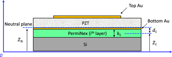
Here, Ei, vi, hi and ρi are Young’s modulus, Poisson’s ratio, thickness, and volume mass density of the ith layer, respectively, and di is the distance from the mid-plane of the ith layer to the neutral plane.
The thickness of each layer is carefully controlled with the consideration of the stress distribution. The neutral plane is designed to be at the bottom of the piezoelectric layer to maximize the transduction, as indicated by [31]:
| (4) |
where the distance from the neutral plane to the reference plane is defined as Zn. Ei, vi, hi and zi are the Young’s modulus, Poisson’s ratio, thickness, and distance from the reference plane to the mid plane of the ith layer, respectively. A schematic diagram of a multilayer pMUT diaphragm for calculating the position of the neutral plane and the equivalent flexural rigidity is shown in Fig. 2. Based on the analysis, the layer stack is designed with the thicknesses listed in Table I. The total thickness of the layer stack is about 9.5 μm.
Fig. 2.
Schematic diagram of a multilayer pMUT diaphragm.
TABLE I.
Layer Thicknesses of the Designed pMUT Array
| Structure | Material | Thickness |
|---|---|---|
| Supporting layer | Si | 3 μm |
| Bonding layer | PermiNex | 2 μm |
| Bottom electrode | Au | 0.1 μm |
| Piezoelectric layer | Ceramic PZT | 4 μm |
| Top electrode | Au | 0.35 μm |
As the resonant frequency of a pMUT is dependent on its dimensions, by tuning the radius of the pMUT diaphragm, various resonant frequencies can be obtained. In this work, 1.3 MHz and 3.5 MHz are the target resonant frequencies since they can be used to detect deeply located tumors and visualize their blood vessels with high resolution for breast cancer imaging applications [32], [33]. According to Eq. (1), the diameters of the pMUT diaphragms for the resonant frequencies of 1.3 MHz and 3.5 MHz are around 240 μm and 146 μm, respectively, corresponding to the diameter-to-thickness ratios of 25 and 15, respectively. It can be seen that the diameter-to-thickness ratio of the higher-frequency pMUT is less than 20, so the simple plate theory is no longer valid. Thus, finite element method (FEM) simulation is also performed to guide the structure design. Starting from the calculated values, multiple iterations are performed in COMSOL Multiphysics software (COMSOL Inc., Burlington, USA) to accurately find the corresponding device dimensions for the target frequencies. It has been found that the diaphragms with the diameters of 220 μm and 120 μm yield the fundamental-mode resonant frequencies of 1.32 MHz and 3.52 MHz, respectively. Thus, 220 μm and 120 μm are selected as the diameter for the designed lower-frequency and higher-frequency pMUTs, respectively. The diameters of the top electrodes for the lower-frequency and higher-frequency pMUTs are 143 μm and 78 μm, respectively, which are designed with a 65% diameter coverage of the diaphragms for optimal sensitivities [21]. Only a 2 × 2 pMUT array, i.e., 1/64 of the entire dual-frequency pMUT array is simulated. The fundamental modes of the lower-frequency and higher-frequency pMUTs are illustrated in Fig. 3(a) and 3(b), respectively. The pitches of the pMUT array are designed to be 380 μm in both axes, leaving adequate space for routing dense top electrodes with a line width of 20 μm. This work is focused on exploring the feasibility of integrating pMUTs with largely separated resonant frequencies. The pitch optimization, directivity and acceptance angle issues are not considered in this paper, which will be thoroughly studied.
Fig. 3.
COMSOL simulation and visualization of the fundamental modes of (a) the lower-frequency and (b) the higher-frequency pMUT elements.
C. Lumped Element Model
Lumped element modeling (LEM) provides a simple and powerful tool for designing and analyzing multiphysics systems as well as predicting their dynamic responses. LEM is efficient since it can simplify the description of spatially distributed physical systems by using a set of lumped elements under certain assumptions. In this method, an LEM has been built for the pMUT to analyze its frequency response and sensitivity.
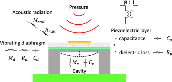
The illustration of the pMUT structure with the lumped elements in the LEM is shown in Fig. 4, which includes the acoustic radiation from the medium, the vibrating diaphragm, and the acoustic cavity. In the acoustic domain, the radiation impedance from the medium is modeled by the resistance Ra,rad and the radiation mass Ma,rad. The air volume in the cavity is modeled as an acoustic mass, Ma,c, and a compliance, Ca,c. In the mechanical domain, the vibrating diaphragm is modeled as a mass-spring-damper system with Mm,d, Cm,d, and Rm,d representing the equivalent mass, compliance, and damping of the diaphragm, respectively. In the electrical domain, the piezoelectric layer is modeled as Ce,p and Re,p, representing the capacitance and dielectric loss, respectively.
Fig. 4.
Illustration of the pMUT structure with lumped elements.
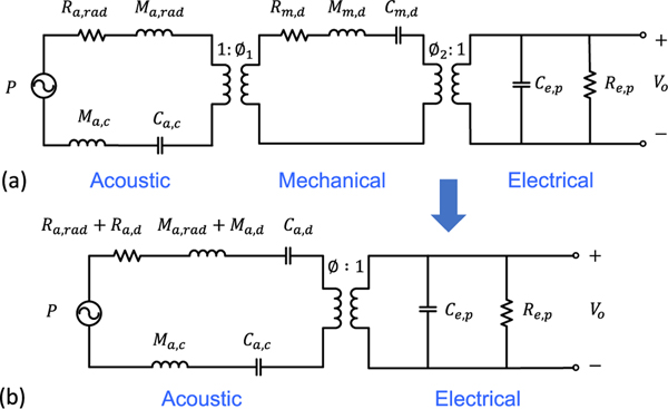
Based on these lumped elements, a complete equivalent circuit in the LEM has been built, as shown in Fig. 5. In the equivalent circuit, the elements that share a common effort are connected in parallel, whereas those sharing a common flow are connected in series. In the acoustic domain, the effort is pressure [Pa] and the flow is volume velocity [m3/s]. In the mechanical domain, the effort is the force [N] and the flow is the particle velocity [m/s]. In the electrical domain, the effort is voltage [V] and the flow is current [A]. The electrical and mechanical domains are coupled by the piezoelectric effects, while the mechanical and acoustic domains are coupled with the effective area of the diaphragm.
Fig. 5.
Equivalent circuit model of pMUTs in (a) three domains and (b) two domains.
For a clamped circular diaphragm, by integrating the velocity distribution over the diaphragm and setting the velocity of the diaphragm as the value at the center point of the diaphragm, Ø1 can be obtained and it turns out to be the effective area, S, of the diaphragm, which is equal to one third of the surface area of the diaphragm. With Ø1 known, the lumped elements in the mechanical domain can be transformed into the acoustic domain, so the equivalent circuit model in Fig. 5(a) can be reduced to two domains, i.e., electrical and acoustic domains, as shown in Fig. 5(b).
The lumped parameters in the equivalent circuit can be derived based on the equations given in [34], [35]. The deflection of the pMUT diaphragm under a pressure or voltage load is also required to solve these equations, which is calculated based on a mechanical model of the diaphragm as described in [36]. Since the deflection of the pMUT diaphragm is modeled based on the classical laminated plate theory, which requires a large diameter to thickness ratio, only the lower-frequency pMUT is analyzed using the LEM.
Based on the equivalent circuit model shown in Fig. 5(b) and the derived lumped elements, the frequency response of the pMUT can be predicted using standard circuit analysis techniques. In this circuit, the pressure and voltage are the input and output, respectively. Thus, the transfer function can be derived representing the transduction gain of the pMUT in the unit of [V/Pa].
First, the impedances from the pMUT diaphragm, Za,d, acoustic cavity, Za,c, and piezoelectric layer, Ze,p, can be calculated as:
| (5) |
| (6) |
| (7) |
Next, the frequency response transfer function relating the open-circuit output voltage to the input pressure is derived via circuit analysis, which is given by:
| (8) |
With the values of the lumped parameters calculated both in air and in water, the transfer function representing the sensitivity of the lower-frequency pMUT is calculated in Matlab (MathWorks Inc., Natick, USA). The result is plotted in Fig. 6, showing the maximum sensitivities of 5.78 μV/Pa and 64 μV/Pa at the resonances of around 865 kHz in water and 1.3 MHz in air, respectively. Due to the added radiation mass in water, the resonant frequency and the maximum sensitivity of the pMUT are smaller in water than in air.
Fig. 6.
Frequency response of the lower-frequency pMUT predicted by LEM.
The use of LEM requires the characteristic length scales of the governing physical phenomena to be much larger than the length scale of interest. In photoacoustic imaging, the acoustic speed in the tissue is around 1500 m/s, so the wavelength of a 1 MHz ultrasonic wave is around 1500 μm, which is about 7 times as large as the diameter of the designed lower-frequency pMUT (220 μm). Thus, LEM can be applied here. However, the prediction of the LEM in air may not be perfect since the acoustic wavelength of a 1 MHz ultrasonic wave in air (343 μm) is only about 1.6 times as large as the diameter of the designed pMUT.
III. Fabrication
The dual-frequency pMUT array is fabricated via a simple three-mask process starting from a 500 μm-thick ceramic PZT wafer (PZT-5H, CTS Inc., USA). Since the pMUT array is designed based on thin ceramic PZT, thinning and integration of ceramic PZT is critical in the fabrication, which is achieved by wafer bonding and chemical mechanical polishing (CMP) techniques. Fig. 7 shows the fabrication process flow in cross-sectional view. Firstly, the ceramic PZT wafer is temporarily bonded with a silicon wafer using SU-8 photoresist (Fig. 7(a)) and polished down to a thickness of around 100 μm with a smooth surface, which is required for depositing metals and obtaining strong bonding strength in the permanent bonding step (Fig. 7(b)). Next, the bottom electrode is deposited by sputtering Au with Cr as the adhesion layer. After that, PermiNex is spin coated on both the PZT wafer and an SOI wafer as the adhesion layers, and then the two wafers are permanently bonded together at a temperature of 180 °C, which is well below the Curie temperature (242 °C) of the PZT-5H (Fig. 7(c)). Next, the PZT is further thinned down to the designed thickness with a carefully tuned CMP process from the Si/SU-8 side, by removing Si, SU-8, and PZT in sequence (Fig. 7(d)). After that, the bottom electrode vias are formed by the photolithography #1 and a wet etch of ceramic PZT using diluted fluoroboric acid (HBF4) with a volume ratio of (HBF4:H2O=1:10) [37] (Fig. 7(e)). Then, the top electrode is defined by the photolithography #2 and a Cr/Au sputtering and liftoff process (Fig. 7(f)). Finally, the acoustic cavities of the pMUT array are defined on the backside using a two-side photolithography #3 (Fig. 7(g)) and formed by a deep reactive ion etch (DRIE) of the silicon (Fig. 7(h)). The buried oxide layer is used as the etching stop layer and subsequently removed by vapor hydrofluoric (HF) acid (Fig. 7(i)).
Fig. 7.
Fabrication process flow.
Fig. 8(a) shows an optical image of the fabricated dual-frequency pMUT array, where the chip size is 7 mm × 7 mm. Fig. 8(b), 8(c), and 8(d) are zoom-in scanning electron microscopic (SEM) images of the fabricated device in the front, backside, and cross-sectional views, respectively. The measured thickness of the ceramic PZT layer is around 4 μm. Large grain sizes of around 2 to 3 μm are identified, which is expected and consistent with high piezoelectric constants of ceramic PZT [38].
Fig. 8.
(a) Optical image, and zoom-in SEM images in (b) front, (c) backside, and (d) cross-sectional views of the fabricated dual-frequency pMUT array.
IV. Device Characterization
The dual-frequency pMUT array was characterized in terms of frequency-dependent electrical impedance, mechanical vibration amplitude and mode mapping, and responsivity of ultrasound generation and sensing.
A. Electrical Impedance Measurement
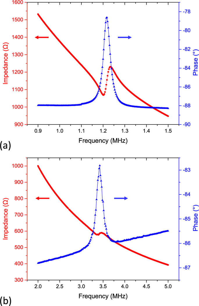
The electrical impedance of the pMUTs was measured in air with an impedance analyzer (4294A, Agilent Inc., USA). Fig. 9(a) and 9(b) show the electrical impedance of a lower-frequency pMUT element and a higher-frequency pMUT element, respectively. As can be seen, the lower-frequency pMUT shows a resonant frequency of 1.20 MHz and an anti-resonant frequency of 1.24 MHz. The higher-frequency pMUT shows the resonance and anti-resonance at 3.38 MHz and 3.48 MHz, respectively. The discrepancies between the measured and simulated resonant frequencies are mainly caused by the cavity dimension change during the fabrication due to the slight sidewall inclination and footing effect in DRIE.
Fig. 9.
The measured electrical impedance of (a) lower-frequency and (b) higher-frequency pMUT elements.
The effective electromechanical coupling coefficient of pMUTs can be calculated based on the measured resonant frequency fr and the anti-resonant frequency fa by:
| (9) |
The calculated are 6.3% and 5.7% for lower-frequency pMUTs and higher-frequency pMUTs, respectively.
B. Mechanical Vibration Test
The mechanical vibration of pMUT elements were measured in air with a digital holographic microscope (DHM-R2100, Lyncee Tec., Switzerland). Firstly, a pMUT element was electrically driven at 6 Vpp with a sweeping frequency, and the vibration amplitudes at different positions of the pMUT diaphragm were measured.
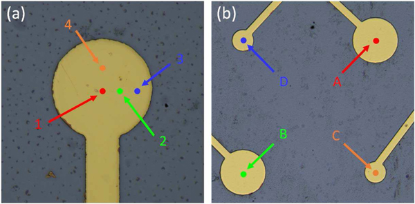
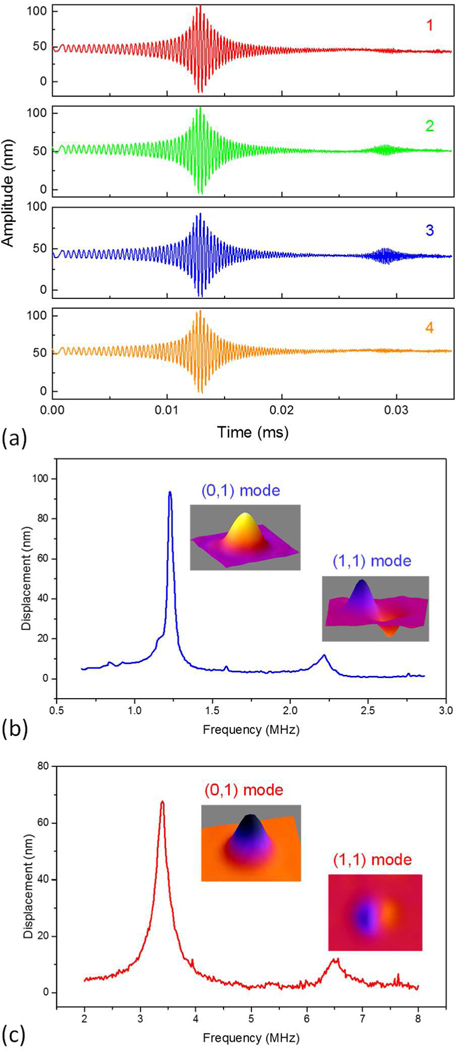
Fig. 10(a) shows a higher-frequency pMUT element with four measuring positions labeled. The corresponding time-domain vibration amplitudes were measured; the results are shown in Fig. 11(a). The measured result at the point 2 was used to calculate the resonance spectrum in frequency domain. Both lower-frequency and higher-frequency pMUT elements were measured and their resonance spectra are shown in Fig. 11(b) and 11(c), respectively. The first resonant frequencies were observed at 1.20 MHz for the lower-frequency pMUT elements and 3.40 MHz for the higher-frequency pMUT elements, which are consistent with the resonant frequencies measured by electrical impedance.
Fig. 10.
pMUT elements with measuring positions labeled: (a) one higher-frequency pMUT element. (b) four adjacent pMUT elements.
Fig. 11.
Measured mechanical vibration: (a) time-domain vibration on a higher-frequency pMUT element. Resonance spectra and mode shapes of (b) a lower-frequency pMUT element and (c) a higher-frequency pMUT element.
Next, the pMUT elements were driven at their resonant frequencies with sine waves to visualize the vibration mode shapes. First two vibration modes were observed, whose mode shapes were reconstructed from the measurement and plotted in Fig. 11(b) and 11(c) for the lower-frequency and higher-frequency pMUT elements, respectively.
Since the dual-frequency pMUT array consists of pMUT elements with different resonant frequencies, cross-coupling (or crosstalk) exists between the interlaced elements with the same and/or different resonant frequencies. Cross-coupling is an undesired effect as it will degrade the performance of transducer arrays. For ultrasonic transmitters, the cross-coupling will cause the distortion of directivity characteristics and affect the beam pattern. For ultrasonic receivers, the cross-coupling will increase the ring down time of the received pulse signals and decrease the imaging resolution. In this work, mechanical vibration tests were performed to evaluate the cross-couplings of the fabricated pMUT arrays.
Firstly, all four adjacent pMUT elements (Fig. 10(b)) were driven simultaneously at either resonant frequency by a sine wave with an amplitude of 2 Vpp. As shown in Fig. 12(a) and 12(b), the lower-frequency and higher-frequency pMUT elements were excited at their own resonances (1.2 MHz and 3.4 MHz, respectively) and their maximum vibration amplitudes were around 100 nm and 30 nm, respectively. It can be seen that the coupling between the two types of pMUTs was not observable.
Fig. 12.
Vibration modes when exciting four adjacent pMUT elements at (a) 1.2 MHz and (b) 3.4 MHz, and exciting (c) one lower-frequency pMUT element at 1.2 MHz and (d) one higher-frequency pMUT element at 3.4 MHz.
Next, experiments were conducted to study the cross-coupling between adjacent pMUT elements with the same resonant frequency. Only one element was excited at its resonance by a sine wave with an amplitude of 2 Vpp, while the vibration displacements at the centers of the four adjacent elements were measured with the vibration mode shapes visualized. Fig. 12(c) and 12(d) show the vibration mode shapes when a lower-frequency and a higher-frequency pMUT element were excited, respectively. Fig. 13(a) and 13(b) show the measured time-domain vibration amplitudes corresponding to the positions labeled in Fig. 10(b), when exciting a lower-frequency pMUT element at 1.2 MHz and a higher-frequency pMUT element at 3.4 MHz, respectively. It can be seen that the cross-coupling between the lower-frequency pMUTs at 1.2 MHz was about 9% (220 nm on the exciting element and 20 nm on the non-exciting element) while the cross-coupling for the higher-frequency pMUTs at 3.4 MHz was less than 5%.
Fig. 13.
Measured cross-coupling level when exciting (a) one lower-frequency pMUT element at 1.2 MHz, and (b) one higher-frequency pMUT element at 3.4 MHz.
Studies have revealed that acoustic propagations in the substrate and the solid-medium interface are the main venues of cross-coupling [39]. By designing mechanical isolation between individual pMUT elements or placing a lossy medium between neighboring elements, the cross-coupling between elements are expected to be mitigated [39]–[41]. These techniques will be implemented in the future designs.
C. Acoustic Sensing Performance
The acoustic sensing performance of the individual elements of the fabricated dual-frequency pMUT array was evaluated by ultrasound transmitting and receiving experiments. A schematic of the experimental setup is shown in Fig. 14, where an off-shelf ultrasonic transmitter (V303, Olympus Inc., Japan) was driven by a function generator to generate ultrasound signals with different frequencies, while the pMUT elements were used as the ultrasound receivers. The pMUT array was assembled on a printed circuit board (PCB). The output signals of the pMUT array were amplified by the circuits on the PCB. The driving signals from the function generator and the amplified output signals from the pMUT were monitored on a digital oscilloscope. The time delay between the two signals was measured on the oscilloscope, which was used to calculate the distance between the ultrasonic transmitter and the pMUT receiver.
Fig. 14.
Schematic of the setup for the ultrasound transmitting and receiving experiments.
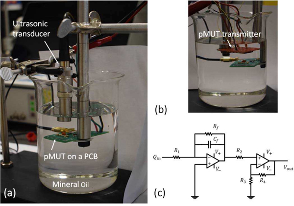
For the lower-frequency pMUT test, a commercial-off-the-shelf immersion-type 1 MHz ultrasonic transducer (V303, Olympus Inc., Japan) was used as the ultrasound transmitter, as shown in Fig. 15(a). For the higher-frequency pMUT test, two fabricated devices were used. Five higher-frequency pMUT elements from one device were connected in parallel as the ultrasound transmitter while one higher-frequency pMUT element from the other device worked as the receiver, as shown in Fig. 15(b). Since pMUT is a type of transducer that typically exhibits high electrical impedance and detects weak acoustic signals, a two-stage interface circuit was designed for the pMUT to amplify the signal and match the electrical impedance, whose schematic is shown in Fig. 15(c). The interface circuit consists of a first-stage charge amplifier and a second-stage voltage amplifier to achieve a 30 dB gain. The deigned interface circuit was fabricated on a PCB, where the fabricated pMUT chip was glued and wire bonded. For electrical insulation, the entire PCB was coated with a thin layer of Parylene C (∼200 nm) and mineral oil was used as the coupling medium in the experiment.
Fig. 15.
Photographs of the experimental setup using (a) a commercial-off-the-shelf (COTS) transducer and (b) pMUTs as ultrasound transmitters, and (c) a schematic of the interface circuit.
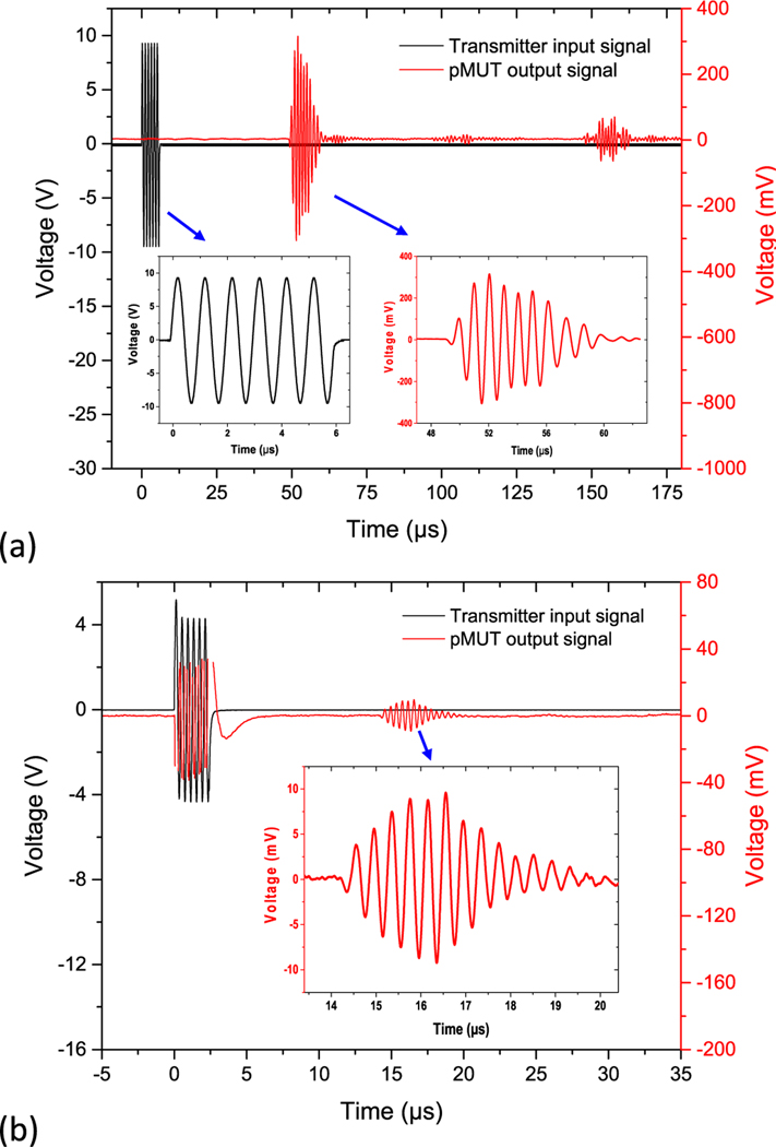
Six sine bursts with frequencies ranging from 0.6 MHz to 3 MHz launched by a function generator were applied to the ultrasound transmitter, while the output signal of the pMUT was synchronized with the driving signal and recorded on an oscilloscope. Due to the electrical impedance mismatch between the function generator and the pMUT transmitter, the maximum output voltage of the function generator decreased with the increasing frequency. Fig. 16(a) shows the testing result of the lower-frequency pMUTs, where a series of 1 MHz sine bursts with an amplitude of 18.8 Vpp were applied, while the pMUT was placed at a distance of 7.5 cm. The acoustic signal reflected between the transmitter and the receiver was also clearly observed, whose acoustic delay was exactly two times of that of the first received signal. Fig. 16(b) shows the testing result of the higher-frequency pMUTs, where 2.5 MHz sine bursts with an amplitude of 8.6 Vpp were applied, while the pMUT receiver was placed at 2 cm away. Compared with the measurement in air, the fundamental resonant frequencies of the dual-frequency pMUT array were reduced to around 0.8 MHz and 2.5 MHz in mineral oil, which can be explained by the added radiation mass from the liquid as [42]:
| (10) |
Fig. 16.
Ultrasound transmitting and receiving results for (a) the lower-frequency pMUTs and (b) the higher-frequency pMUTs.
where foil, fair, Ap, and Mp are the resonant frequencies in mineral oil and in air, the added radiation mass, and the mass of the pMUT diaphragm, respectively.
Electromagnetic interference from the input signals during the transmitting period is also observed in the experiments. As shown in Fig 16, an electromagnetic coupling signal with an amplitude of around 40 mV is observed in the higher-frequency pMUT test, while a much smaller electromagnetic coupling signal with an amplitude of around 10 mV is seen in the lower-frequency pMUT test. The stronger electromagnetic interference in the higher-frequency pMUT test is believed to be caused by the reduced distance between the transmitter and the receiver as well as the packaging and shielding difference between the pMUT transmitter and the commercial ultrasonic transmitter.
Table II gives a comparison of the state-of-the-art pMUTs that have been developed for PAI or can be potentially used for PAI applications. In general, the dual-frequency pMUT array presented in this work have much greater electromechanical coupling factors than other pMUTs due to the superior piezoelectric properties of ceramic PZT. The pMUTs developed in this work also exhibit larger displacement sensitivities than most of other pMUTs with similar sizes.
TABLE II.
Comparison of pMUTS
| Ref. | Piezoelectric Material | Number of Elements | Frequency (MHz) | Element Size (μm) | Max. Trans. Gain (nm/V) | Electromechanical Coupling | |
|---|---|---|---|---|---|---|---|
| Material | Thickness (μm) | ||||||
| [22] | Sol-gel PZT (2% Nb doped) | 1.9 | 65* | 7 | 60 (diameter) | 55 | – |
| [15] | AIN | 0.7 | 6* | 6 | 100 (diameter) | 20 | – |
| [14] | AIN | ~1 | – | 2.9 | – | – | 2.38%–3.71% |
| [43] | AIN | 2 | – | 2.19 | 190 (diameter) | 45 | – |
| [44] | AIN | 1 | – | 2.2 | 200 (length) | 123 | 0.41% |
| [45] | Sol-gel PZT | 2 | 36 | 1 | 200 (length) | – | 2.15% |
| [46] | Sol-gel PZT | 1 | 256 | 0.75 | 100 (length) | 51 | 1.82% |
| [47] | Sol-gel PZT | 1 | 2393 | 1.52 | 120 (diameter) | – | 1.29% |
| [40] | Sputtered PZT | 3 | 120+192 | 0.77 & 2.3 | 410 & 230 (diameter) | 595 & 112 | 4.31% & 5.64% |
| This Work | Ceramic PZT | 4 | 128+128 | 1.2 & 3.4 | 220 & 120 (diameter) | 110 & 30 | 6.3% & 5.7% |
Multiple pMUT diaphragms are connected together to form one pMUT element.
V. Photoacoustic Imaging
A. Experimental Setup
Photoacoustic imaging (PAI) performance of the fabricated dual-frequency pMUT array was validated through PAI experiments with a phantom. The schematic of the experimental system is shown in Fig. 17, which consists of a pulsed laser source, a mechanical scanning subsystem, and an acoustic signal detection and process subsystem. PAI experiments were performed using the fabricated pMUT arrays in a tank filled with deionized (DI) water as the coupling medium. A ‘+’ shaped pattern made of two 0.5 mm-wide pencil leads embedded into an agar phantom (3 cm in diameter and 6 cm in height) was used as the imaging target. As shown in Fig. 17, short laser pulses (6 ns duration and 20 mJ energy per pulse) generated from an OPO laser source (Phocus Mobile, Opotek Inc., USA) with a wavelength of 720 nm were shone on the imaged phantom to generate photoacoustic waves, while the pMUT array packaged on a PCB was controlled by a rotator to scan around the phantom for acquisition of photoacoustic signals. The pMUT array was rotated at a step of 3°C for a full revolution. Totally 120 photoacoustic A-line signals were acquired per revolution by the pMUT. The output signals of the PCB were further amplified using a Pulser/Receiver (5077-PR, Olympus Inc., Japan) with a 26 dB gain and then acquired by a data acquisition (DAQ) board (PCI-5152, National Instruments Inc., USA). The data were processed using a delay and sum algorithm to reconstruct photoacoustic images [48].
Fig. 17.
Schematic illustration of the experimental system for PAI. Inset: a photograph of the phantom (a cross of pencil leads embedded in agar).
Although the fabricated dual-frequency pMUT array had 16 × 16 channels, multiple pMUT elements were wire bonded together to form only two signal channels, one lower-frequency channel and one higher-frequency channel, because the DAQ board had a limited number of channels. A fabricated dual-frequency pMUT array was packaged on a two-channel interface circuit board and wire bonded for PAI experiments, as shown in Fig. 18, where 30 lower-frequency pMUT elements and 30 higher-frequency pMUT elements were employed.
Fig. 18.
Photographs of (a) the wire bonded pMUT array on the PCB, and (b) the experimental configuration.
B. Photoacoustic Signals and Images
Photoacoustic signals were successfully detected by both lower-frequency pMUT elements and higher-frequency pMUT elements, as shown in Fig. 19(a) and 19(b), respectively. For PAI with the lower-frequency pMUTs, the pMUT array was placed as far as 5 cm away from the imaging target and strong signals were detected, as shown in Fig. 19(a). Due to the increased acoustic attenuation and the smaller sensing aperture, the amplitude of the detected photoacoustic signals with the higher-frequency pMUTs was smaller even though the device was placed closer (3 cm) to the imaging target. The bandwidths of the pMUT elements are evaluated by fast Fourier transform (FFT) of the received photoacoustic A-line signals. The results are plotted in Fig. 19, showing that the center frequency and −6 dB bandwidth are 0.84 MHz and 54% for the lower-frequency pMUT elements, and 2.4 MHz and 17% for the higher-frequency pMUT elements, respectively.
Fig. 19.
Photoacoustic signals detected by (a) the lower-frequency pMUTs and (b) the higher-frequency pMUTs.
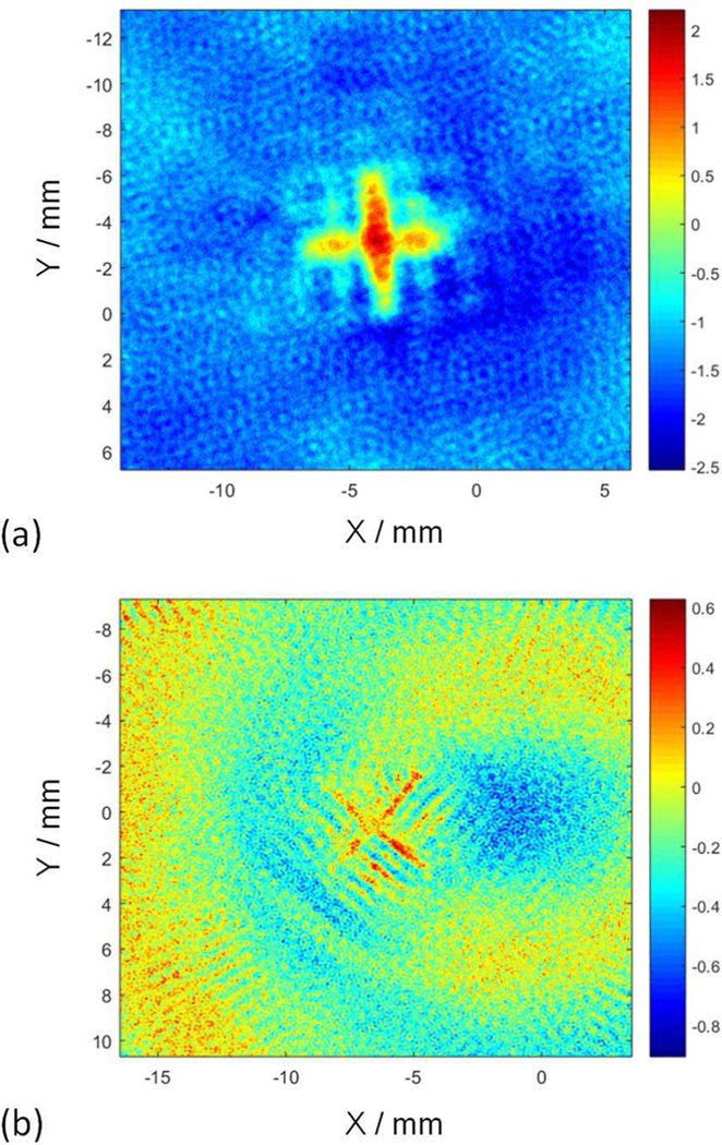
Photoacoustic images were reconstructed based on the signals detected by both the lower-frequency pMUTs and the higher-frequency pMUTs, as shown in Fig. 20(a) and 20(b), respectively. The cross (‘+’) shaped pattern of the two pencil leads can be identified from both reconstructed images, but their contrasts and resolutions are different. The reconstructed image based on the signals from the lower-frequency pMUTs shows a high contrast but a poor resolution. The high contrast is consistent with the large amplitude of the detected photoacoustic signal shown in Fig. 19(a), while the poor resolution is caused by the low resonant frequency of the applied pMUTs. By contrast, the reconstructed image based on the signals from the higher-frequency pMUTs exhibits higher resolution and provides better accuracy of the target size. However, it has a lower contrast due to the smaller amplitude and lower signal-to-noise ratio (SNR) in the detected photoacoustic signals.
Fig. 20.
Reconstructed photoacoustic images based on signals from (a) the lower-frequency pMUTs and (b) the higher-frequency pMUTs.
VI. Conclusion
A 16 × 16 dual-frequency pMUT array based on thin ceramic PZT has been successfully designed, modeled, fabricated, and experimentally verified for endoscopic PAI applications. The dual-frequency characteristics of the fabricated device have been evaluated with electrical impedance measurement, mechanical vibration tests, acoustic sensing and PAI experiments. High effective electromechanical coupling factors of 6.3% and 5.7% have been obtained for lower- and higher- frequency pMUT elements, respectively. The lower-frequency and higher-frequency pMUT elements show maximum voltage-to-displacement transduction gains (responsivities) of 110 nm/V and 30 nm/V with cross-couplings of about 9% and 5% at their resonances of 1.2 MHz and 3.4 MHz, respectively. Photoacoustic signals of pencil-lead patterns embedded into an agar phantom have been successfully detected by the dual-frequency pMUT array. The reconstructed photoacoustic images clearly identify the embedded pencil-lead patterns and the imaging contrast and spatial resolution are obviously frequency dependent. These results have demonstrated the great potential of applying such dual-frequency pMUT arrays for endoscopic PAI that can provide high spatial resolution and large imaging depth simultaneously.
In the future, it appears feasible a hydrophone may be used to calibrate the receive sensitivity of pMUTs in μV/Pa, and photoacoustic images reconstructed by lower-frequency and higher-frequency pMUTs may be combined with suitable algorithms, to obtain a photoacoustic image with both high resolution and high contrast.
Acknowledgments
This work was supported by the National Institutes of Health (NIH) under the award #R01EB020601.
Biographies

Haoran Wang received his B.S. degree in measuring and control technology and instruments from Tianjin University, Tianjin, China, in 2017, and the Ph.D. degree in electrical and computer engineering from University of Florida, Gainesville, USA, in 2021. His research interests include microelectromechanical systems (MEMS), optical MEMS, micro/nano fabrication, and piezoelectric transducers.

Hao Yang received his B.E. and Ph.D. degree in optical engineering from Sichuan University, Chengdu, China, in 2010. He is currently working as a research professor in the Department of Medical Engineering at University of South Florida, Tampa, USA. His research interests include optical-based imaging technologies for in vivo visualization of tissue at both the macroscopic and microscopic scales.

Zhenfang Chen, founder of MEMS Engineering & Material which develops and manufactures SOI wafers and other bonded material for MEMS and semiconductor applications. Prior to this, he worked as the principle engineer for Fujifilm Dimatix, Santa Clara, California. He received Ph.D. in metallurgical physical chemistry from Central South University, Changsha, China.

Qincheng Zheng is an undergraduate student in the School of Information and Electronics, Beijing Institute of Technology, majoring in Electronic Science and Technology. His research interests include microelectromechanical systems (MEMS), micro/nano fabrication, and piezoelectric micromachined ultrasound transducers.

Huabei Jiang, PhD, started his career as an Assistant Professor of physics at Clemson University in 1997, and became a full Professor there in 2003. He then joined University of Florida (UF) in 2005 as a founding senior faculty of then newly established biomedical engineering department and became the J. Crayton Pruitt Family endowed professor in 2008 at UF. Dr. Jiang joined University of South Florida (USF) in 2017 as a founding faculty of medical engineering department and the founding Director of USF Center for Advanced Biomedical Imaging. Professor Jiang has published over 400 peer-reviewed scientific articles and patents. He is also the author of three books, Diffuse Optical Tomography: Principles and Applications (CRC Press, 2010), Photoacoustic Tomography (CRC Press, 2014), and Thermoacoustic Tomography: Principles and Applications (IOP Publishing, 2020). Huabei Jiang is a Fellow of the Optical Society of America (OSA), a Fellow of the International Society of Optical Engineering (SPIE), and a Fellow of the American Institute of Medical and Biological Engineering (AIMBE). Outside his research/teaching, Huabei Jiang spends much of his time practicing Chinese Calligraphy and painting (ink/color pencil and watercolor). He has had the first exhibition of his artworks in July 2019 in Chengdu, China.

Philip X.-L. Feng (Senior Member, IEEE) received his Ph.D. degree in Electrical Engineering (EE) from the California Institute of Technology (Caltech), Pasadena, CA, in 2007. He is currently a Professor in the Department of Electrical and Computer Engineering, University of Florida, Gainesville, Florida, USA. His research is primarily focused on emerging solid-state devices and systems, particularly nano/microelectromechanical systems (NEMS/MEMS), atomic layer semiconductors and 2D devices, silicon carbide (SiC) and other advanced semiconductors, quantum devices based on SiC and 2D materials, as well as their integration with state-of-the-art ICs and optical/photonic technologies. He is an alumnus of the National Academy of Engineering (NAE) U.S. Frontier of Engineering (USFOE) program and subsequently a recipient of the NAE Grainger Foundation Frontiers of Engineering (FOE) Award. His awards also include the Presidential Early Career Award for Scientists and Engineers (PECASE 2019) and the National Science Foundation CAREER Award (2015). He and his students has won four Best Paper/Presentation Awards at IEEE and other international conferences. He has mentored over ten Ph.D. students to successful dissertation defense, and also supervised eight M.S. students with thesis research. He has served on the Technical Program Committees (TPCs) for the IEEE International Electron Devices Meeting (IEDM), the IEEE International Conference on Micro Electro Mechanical Systems (MEMS), International Conference on Solid-State Sensors, Actuators and Microsystems (Transducers), and other international conferences. He served as a Track Chair for IEEE SENSORS 2016–2017, and as the TPC Group Chair for the IEEE IFCS 2018, IFCS-EFTF 2019, and IFCS-ISAF 2020. He has also served as the Technical Program Chair for the MEMS/NEMS Technical Group at the 61st to 63rd American Vacuum Society (AVS) International Symposium & Exhibition. He is a co-organizer and the technical chair of the SiC Materials & Devices Workshop (since 2017). He has served as a Chair for the 34th IEEE International Conference on Micro Electro Mechanical Systems (IEEE MEMS 2021).

Huikai Xie (Fellow, IEEE) is a Professor at the School of Information and Electronics, Beijing Institute of Technology, Beijing, China. He received his B.S. in microelectronics, M.S. in photonics, and Ph.D. in electrical and computer engineering from Beijing Institute of Technology, Tufts University, and Carnegie Mellon University, respectively. He worked at University of Florida as an assistant professor (2002–2007), associate professor with tenure (2007–2011) and full professor (2011–2020). He has published over 300 technical papers and 11 book chapters and holds over 30 US patents. His current research interests include MEMS/NEMS, optical beam steering, optical communications, LiDAR, NIR spectroscopy, and optical microendoscopy. He is the founder of Wuxi WiO Technologies Co., Ltd. He is an associate editor of the IEEE Sensors Letters and Sensors & Actuators A. He is a fellow of IEEE and SPIE.
Contributor Information
Haoran Wang, Department of Electrical and Computer Engineering, University of Florida, Gainesville, FL 32611, USA.
Hao Yang, Department of Medical Engineering, University of South Florida, Tampa, FL 33620, USA.
Zhenfang Chen, MEMS Engineering and Materials Inc., Sunnyvale, CA 94086, USA.
Qincheng Zheng, School of Information and Electronics, Beijing Institute of Technology, Beijing 100081, China.
Huabei Jiang, Department of Medical Engineering, University of South Florida, Tampa, FL 33620, USA.
Philip X.-L. Feng, Department of Electrical and Computer Engineering, University of Florida, Gainesville, FL 32611, USA.
Huikai Xie, School of Information and Electronics, Beijing Institute of Technology, Beijing 100081, China; BIT Chongqing Center of Microelectronics and Microsystems, Chongqing, 400030, China..
REFERENCES
- [1].Mallidi S, Luke GP, and Emelianov S, “Photoacoustic imaging in cancer detection, diagnosis, and treatment guidance,” Trends in Biotechnol., vol. 29, no. 5, pp. 213–221, 2011. [DOI] [PMC free article] [PubMed] [Google Scholar]
- [2].Yao J and Wang LV, “Photoacoustic brain imaging: from microscopic to macroscopic scales,” Neurophotonics, vol. 1, art. no. 011003, 2014. [DOI] [PMC free article] [PubMed] [Google Scholar]
- [3].Yang J, Zhang G, Wu M, Shang Q, Huang L, and Jiang H, “Photoacoustic assessment of hemodynamic changes in foot vessels,” J. Biophotonics, vol. 12, art. no. e201900004, 2019. [DOI] [PubMed] [Google Scholar]
- [4].Xi L and Jiang H, “High resolution three-dimensional photoacoustic imaging of human finger joins in vivo,” Appl. Phys. Lett, vol. 107, art. no. 063701, 2015. [Google Scholar]
- [5].Zackrisson S, van de Ven SMWY, and Gambhir SS, “Light in and sound out: emerging translational strategies for photoacoustic imaging,” Cancer Res., vol. 74, no. 4, pp. 979–1004, 2014. [DOI] [PMC free article] [PubMed] [Google Scholar]
- [6].Xu M and Wang LV, “Photoacoustic imaging in biomedicine,” Rev. Sci. Instrum, vol. 77, art. no. 041101, 2006. [Google Scholar]
- [7].Li X, Heldermon CD, Yao L, Xi L, and Jiang H, “High resolution functional photoacoustic tomography of breast cancer,” Med. Phys, vol. 42, no. 9, pp. 5321–5328, 2015. [DOI] [PubMed] [Google Scholar]
- [8].Upputuri PK and Pramanik M, “Recent advances toward preclinical and clinical translation of photoacoustic tomography: a review,” J. Biomed. Opt, vol. 22, art. no. 041006, 2017. [DOI] [PubMed] [Google Scholar]
- [9].Guo H, Li Y, Qi W, and Xi L, “Photoacoustic endoscopy: A progress review,” J. Biophotonics, vol. 13, art. no. e202000217, 2020. [DOI] [PubMed] [Google Scholar]
- [10].Wang LV and Hu S, “Photoacoustic tomography: in vivo imaging from organelles to organs.” Science, vol. 335, pp. 1458–1462, 2012. [DOI] [PMC free article] [PubMed] [Google Scholar]
- [11].Wang H, Ma Y, Yang H, Jiang H, Ding Y, and Xie H, “MEMS ultrasound transducers for endoscopic photoacoustic imaging applications,” Micromachines, vol. 11, art. no. 928, 2020. [DOI] [PMC free article] [PubMed] [Google Scholar]
- [12].Vaithilingam S et al. , “Three-dimensional photoacoustic imaging using a two-dimensional CMUT array,” IEEE Trans. Ultrason. Ferroelectr. Freq. Control, vol. 56, no. 11, pp. 2411–2419, 2009. [DOI] [PubMed] [Google Scholar]
- [13].Ilkhechi AK, Ceroici C, Li Z, and Zemp R, “Transparent capacitive micromachined ultrasonic transducer (CMUT) arrays for real-time photoacoustic applications,” Opt. Express, vol. 28, no. 9, pp. 13750–13760, 2020. [DOI] [PubMed] [Google Scholar]
- [14].Chen B, Chu F, Liu X, Li Y, Rong J, and Jiang H, “AlN-based piezoelectric micromachined ultrasonic transducer for photoacoustic imaging,” Appl. Phys. Lett, vol. 103, art. no. 031118, 2013. [Google Scholar]
- [15].Dangi A et al. , “Ring PMUT array based miniaturized photoacoustic endoscopy device,” SPIE Proceedings of Photons Plus Ultrasound: Imaging and Sensing, 2019, art. no. 1087811. [Google Scholar]
- [16].Pun SH et al. , “Monolithic multiband cMUTs for photoacoustic computed tomography with in vivo biological tissue imaging,” IEEE Trans. Ultrason. Ferroelectr. Freq. Control, vol. 65, no. 3, pp. 465–475, 2018. [DOI] [PubMed] [Google Scholar]
- [17].Chee RKW, Zhang P, Maadi M, and Zemp RJ, “Multifrequency interlaced cMUTs for photoacoustic imaging,” IEEE Trans. Ultrason. Ferroelectr. Freq. Control, vol. 64, no. 2, pp. 391–401, 2017. [DOI] [PubMed] [Google Scholar]
- [18].Qiu Y et al. , “Piezoelectric micromachined ultrasound transducer (PMUT) arrays for integrated sensing, actuation and imaging,” Sensors, vol. 15, pp. 8020–8041, 2015. [DOI] [PMC free article] [PubMed] [Google Scholar]
- [19].Ozaki K, Matin A, Numata Y, Akai D, Sawada K, and Ishida M, “Fabrication and characterization of a smart epitaxial piezoelectric micromachined ultrasonic transducer,” Mater. Sci. Eng. B, vol. 190, pp. 41–46, 2014. [Google Scholar]
- [20].Wang Q, Lu Y, Mishin S, Oshmyansky Y, and Horsley DA, “Design, fabrication, and characterization of scandium aluminum nitride-based piezoelectric micromachined ultrasonic transducers,” J. Microelectromech. Syst, vol. 26, no. 5, pp. 1132–1139, 2017. [Google Scholar]
- [21].Muralt P et al. , “Piezoelectric micromachined ultrasonic transducers based on PZT thin films,” IEEE Trans. Ultrason. Ferroelectr. Freq. Control, vol. 52, no. 12, pp. 2276–2288, 2005. [DOI] [PubMed] [Google Scholar]
- [22].Dangi A et al. , “A photoacoustic imaging device using piezoelectric micromachined ultrasound transducers (PMUTs),” IEEE Trans. Ultrason. Ferroelectr. Freq. Control, vol. 67, no. 4, pp. 801–809, 2020. [DOI] [PMC free article] [PubMed] [Google Scholar]
- [23].Wang H, Chen Z, Yang H, Jiang H, and Xie H, “A ceramic PZT-based pMUT array for endoscopic photoacoustic imaging,” J. Microelectromech. Syst, vol. 29, no. 5, pp. 1038–1043, 2020. [DOI] [PMC free article] [PubMed] [Google Scholar]
- [24].Wang H, Feng PX-L, and Xie H, “A high-density and dual-frequency pMUT array based on thin ceramic PZT for endoscopic photoacoustic imaging,” The 34th Int. Conf. Micro Electro Mech. Syst. (MEMS), 2021, pp. 891–894. [DOI] [PMC free article] [PubMed] [Google Scholar]
- [25].Wang Z, Miao J, Tan CW, and Xu T, “Fabrication of piezoelectric MEMS devices-from thin film to bulk PZT wafer,” J. Electroceram, vol. 24, pp. 25–32, 2010. [Google Scholar]
- [26].Wang H, Yu Y, Chen Z, Yang H, Jiang H, and Xie H, “Design and fabrication of a piezoelectric micromachined ultrasonic transducer array based on ceramic PZT,” IEEE Sensors Conf., 2018. [Google Scholar]
- [27].Ebrahimi F and Rastgo A, “An analytical study on the free vibration of smart circular thin FGM plate based on classical plate theory,” Thin-Walled Struct., vol. 48, pp. 1402–1408, 2008. [Google Scholar]
- [28].Liu X, Wang Q, and Quek ST, “Analytical solution for free vibration of piezoelectric coupled moderately thick circular plates,” Int. J. Solids Struct, vol. 39, pp. 2129–2151, 2002. [Google Scholar]
- [29].Lu Y and Horsley DA, “Modeling, fabrication, and characterization of piezoelectric micromachined ultrasonic transducer arrays based on cavity SOI wafers,” J. Microelectromech. Syst, vol. 24, no. 4, pp. 1142–1149, 2015. [Google Scholar]
- [30].Dangi A and Pratap R, “System level modeling and design maps of PMUTs with residual stresses,” Sens. Actuators A, Phys, vol. 262, pp. 18–28, 2017. [Google Scholar]
- [31].Sammoura F, Smyth K, Bathurst S, and Kim S-G, “An analytical analysis of the sensitivity of circular piezoelectric micromachined ultrasonic transducers to residual stress,” IEEE Int. Ultrason. Symp, 2012, pp 580–583. [Google Scholar]
- [32].Manohar S et al. , “Initial results of in vivo non-invasive cancer imaging in the human breast using near-infrared photoacoustics,” Opt. Express, vol. 15, no. 19, pp. 12277–12285, 2007. [DOI] [PubMed] [Google Scholar]
- [33].Lin L et al. , “Single-breath-hold photoacoustic computed tomography of the breast,” Nat. Commun, vol. 9, art. no. 2352, 2018. [DOI] [PMC free article] [PubMed] [Google Scholar]
- [34].Williams MD, Griffin BA, Reagan TN, Underbrink JR, and Sheplak M, “An AlN MEMS piezoelectric microphone for aeroacoustic applications,” J. Microelectromech. Syst, vol. 21, no. 2, pp. 270–283, 2012. [Google Scholar]
- [35].Horowitz S, Nishida T, Cattafesta L, and Sheplak M, “Development of a micromachined piezoelectric microphone for aeroacoustics applications,” J. Acoust. Soc. Am, vol. 122, pp. 3428–3436, 2007. [DOI] [PubMed] [Google Scholar]
- [36].Deshpande M and Saggere L, “An analytical model and working equations for static deflections of a circular multi-layered diaphragm-type piezoelectric actuator,” Sens. Actuators A, Phys, vol. 136, pp. 673–689, 2007. [Google Scholar]
- [37].Wang H, Godara M, Chen Z, and Xie H, “A one-step residue-free wet etching process of ceramic PZT for piezoelectric transducers,” Sens. Actuators A, Phys, vol. 290, pp. 130–136, 2019. [DOI] [PMC free article] [PubMed] [Google Scholar]
- [38].Randall CA, Kim N, Kucera J-P, Cao W, and Shrout TR, “Intrinsic and extrinsic size effects in the fine-grained morphotropicphas-boundary lead zirconate titanate ceramics,” J. Am. Ceram. Soc, vol. 81, pp. 677–688, 1998. [Google Scholar]
- [39].Jin X, Oralkan Ö, Degertekin FL, and Khuri-Yakub BT, “Characterization of one-dimensional capacitive micromachined ultrasonic immersion transducer arrays,” IEEE Trans. Ultrason. Ferroelectr. Freq. Control, vol. 48, no. 3, pp. 750–760, 2001. [DOI] [PubMed] [Google Scholar]
- [40].Liu L et al. , “A dual-frequency piezoelectric micromachined ultrasound transducer array with low inter-element coupling effects,” J. Micromech. Microeng, vol. 31, art. no. 045005, 2021. [Google Scholar]
- [41].Xu T et al. , “Array design of piezoelectric micromachined ultrasonic transducers with low-crosstalk and high-emission performance,” IEEE Trans. Ultrason. Ferroelectr. Freq. Control, vol. 67, no. 4, pp. 789–800, 2020. [DOI] [PubMed] [Google Scholar]
- [42].Blevins RD, Formulas for Natural Frequency and Mode Shape, Van Nostrand Reinhold, New York, USA, 1979. [Google Scholar]
- [43].Akhbari S, Sammoura F, Shelton S, Yang C, Horsley D, and Lin L, “Highly responsive curved aluminum nitride PMUT,” The 27th Int. Conf. Micro Electro Mech. Syst. (MEMS), 2014, pp. 124–127. [Google Scholar]
- [44].Wang T and Lee C, “Zero-bending piezoelectric micromachined ultrasonic transducer (pMUT) with enhanced transmitting performance,” J. Microelectromech. Syst, vol. 24, no. 6, pp. 2083–2091, 2015. [Google Scholar]
- [45].Yang Y et al. , “An ultra-high element density pMUT array with low crosstalk for 3-D medical imaging,” Sensors, vol. 13, pp. 9624–9634, 2013. [DOI] [PMC free article] [PubMed] [Google Scholar]
- [46].Ling J et al. , “Design and characterization of high-density ultrasonic transducer array,” IEEE Sens. J, vol. 18, no. 6, pp. 2285–2290, 2018. [Google Scholar]
- [47].Jung J et al. , “A top-crossover-to-bottom addressed segmented annular array using piezoelectric micromachined ultrasonic transducers,” J. Micromech. Microeng, vol. 25, art. no. 115024, 2015. [Google Scholar]
- [48].Hoelen CGA and de Mul FFM, “Image reconstruction for photoacoustic scanning of tissue structures,” Appl. Opt, vol. 39, no. 31, pp. 5872–5883, 2000. [DOI] [PubMed] [Google Scholar]


