Abstract
This paper presents for the first time a p-type 4H silicon carbide (4H-SiC) van der Pauw strain sensor by utilizing the strain induced effect in four-terminal devices. The sensor was fabricated from a 4H-SiC (0001) wafer, using a 1 μm thick p-type epilayer with a concentration of 1018 cm−3. Taking advantage of the four-terminal configuration, the sensor can eliminate the need for resistance-to-voltage conversion which is typically required for two-terminal devices. The van der Pauw sensor also exhibits an excellent repeatability and linearity with a significantly large output voltage in induced strain ranging from 0 to 334 ppm. Various sensors aligned in different orientations were measured and a high sensitivity of 26.3 ppm−1 was obtained. Combining these performances with the excellent mechanical strength, electrical conductivity, thermal stability, and chemical inertness of 4H-SiC, the proposed sensor is promising for strain monitoring in harsh environments.
This paper presents for the first time a p-type 4H silicon carbide (4H-SiC) van der Pauw strain sensor by utilizing the strain induced effect in four-terminal devices.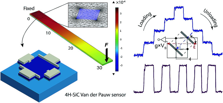
Introduction
Silicon carbide (SiC) is a favorable material for high power and electronics devices, and high temperature applications owing to its wide energy-band gap, high break-down voltage, good electrical conductivity, and thermal stability. Taking advantage of the superior properties and availability of SiC wafers, SiC-based MEMS mechanical sensors have been developed for harsh environments. Specifically, SiC-based pressure sensors, accelerometers and strain sensors have been reported with a good performance even when operating at high temperatures.1–5 Possessing a superior large energy-band gap (2.3–3.2 eV), SiC-based devices can operate at higher temperatures by eliminating the thermally induced leakage of the minority carriers.6 Among more than two hundred SiC polytypes, 4H-SiC is favorable for MEMS devices owing to its excellent properties7,8 and commercial availability. 4H-SiC possesses the highest energy-band gap of 3.23 eV in comparison with other SiC polytypes, minimizing the number of electron–hole pairs formed in thermal activation across the bandgap, enabling the high temperature stability of 4H-SiC electronic devices and sensors.9
The strain induced effect on the resistivity (i.e. piezoresistive effect) of two-terminal SiC devices has been reported for mechanical sensing applications with relatively high gauge factors (GF).10–14 However, resistance-to-voltage and signal-amplification circuitries are typically required for converting resistance changes to output voltages, creating issues in terms of measurement configurations, as well as exhibiting higher signal noises and delays.15,16 Additionally, the difference in the temperature coefficient of the four resistors constructing the Wheatstone bridge circuit, leads to a non-zero offset during operations with varying temperature, hindering the sensitivity of the sensors. Moreover, the thermal coefficient of resistance (TCR) contributes significantly to the measurement of two-terminal devices.16 This results in a reduction in the signal-to-noise ratio and hinders the reliability of strain sensors. In contrast, the variation in respect to the temperature change is minimized in four-terminal devices since the TCR of piezoresistors would be cancelled out. There are numerous studies on the 3C-SiC based four-terminal strain sensor with a relatively high sensitivity and good reproducibility.15–21 However, the strain induced effect and strain sensing in four-terminal 4H-SiC have not been investigated. Yet, the development of SiC devices and electronics is shifting towards 4H-SiC and 6H-SiC, which are widely available. These raise the need for the investigation of the strain induced effect in such devices. Therefore, understanding this phenomenon in 4H-SiC is of great interest for the development of highly sensitive, circuit conversion-free strain sensors which have superior performances even in high temperature operations.
This work presents a 4H-SiC van der Pauw (4HVP) strain sensor, with a four-terminal configuration, with excellent performance including a good repeatability, linearity and high sensitivity. The use of a four-terminal structure eliminates the need for the resistance-to-voltage conversion. The orientation dependence of the sensor in the 4H-SiC (0001) wafer was also investigated to obtain the high sensitivity of 26.3 ppm−1.
Fabrication of the van der Pauw sensor
The sensors were fabricated from a 4H-SiC (0001) wafer (sourced Ascatron™) which is has 4° off-cut surface from the basal plane (0001) towards the 〈112̄0〉 orientation. The 4H-SiC wafer has a thickness of 350 μm, consisting of 1 μm p-type epilayer, 1 μm n-type buffer layer, and a low-doped n-type substrate. The p-type layer was formed using aluminum dopants, with a concentration of 1018 cm−3, while doping concentration of the n-type layer was also 1018 cm−3 with nitrogen dopants. Fig. 1(a) summarizes the fabrication process of the p-type 4HVP sensors. The process started with a standard wafer cleaning procedure then spin coating/developing 4.3 μm-thick AZ9245 photoresist by a standard lithography process to create a protective mask for the subsequent etching of the p-type layer (step ②). Inductive coupled plasma (ICP) etching was performed to etch p-type 4H-SiC using a STS™ etcher (step ③). The plasma etching employed HCl (500 sccm) at a low pressure of 2 mTorr and the wafer was continuously cooled down by back-side gas cooling in the etching chamber. The etch rate was measured at approximately 100 nm-per-minute and the final etched depth of 1.3 μm was achieved. This ensures that the 1 μm p-type layer was thoroughly etched in the designated area; then mesa square-shape structures were formed on the p-type layer. Titanium and aluminum metal layers were subsequently deposited to form a contact for the sensor, using a SNS™ sputterer with the thickness of each layer being 100 nm. Next, a second photoresist mask was formed on top of the as-etched p-type 4H-SiC patterns (step ④), followed by a wet etching of Ti/Al to create the designated metal contact for subsequent electrical measurements (step ⑤). An annealing process at high temperature up to 1000 °C was conducted to obtain a good ohmic contact. The detailed annealing process can be found in our previous paper.22 Finally, the wafer was diced into 30 mm × 3 mm × 0.35 mm beams which were aligned to the 〈11̄00〉 direction.
Fig. 1. (a) Fabrication of the 4HVP sensor. (b) Ohmic contact characteristics of Ti/Al contact. Inset: top-to-top current leakage.
Results and discussion
Fig. 1(b) shows a good linearity of the current–voltage characteristics of the annealed Ti/Al contact to p-type 4H-SiC in the voltage range from −2 to 2 V using a Keithley 2602B System SourceMeter™. Accordingly, the resistivity of the p-type layer was found to be 0.91 Ω cm. Since strain sensors typically operate in small voltage ranges (e.g. below ±1 V) to avoid the Joule heating effect, the measured I–V characteristics in the given range is sufficient for strain sensing applications. It is also necessary to investigate the current leakage through the p–n junction to the n-type layer and the substrate. As can be seen in Fig. 1(b) inset, when sweeping bias voltages from −2 to 2 V, the leakage current to the n-type layer and the substrate is in the range of tens of pico amperes (pA) which is seven orders of magnitude smaller than the current in the sensor (e.g. hundreds of micro amperes (μA)). This is attributed to the fact that the back-to-back p–n diode prevents the current from leaking into the n-type layer and the substrate.7,22 In our previous study,22 we have formed an ohmic contact to the n-type substrate and investigated the vertical current leakage from the epi-layer (p-type) to the bulk substrate (n-type), showing a small current in the nA order. This result indicated that the n-type substrate did not have a significant contribution on the change in the p-type van der Pawn devices under strain. Consequently, the contribution of the underneath layers other than the p-type layer to the electrical measurements of the devices, can be negligible.
To investigate the orientation dependence of the sensors to the induced strain, the p-type 4HVP sensors were aligned to three different orientations which are 0°, 45°, and 90° to 〈11̄00〉 orientation (Fig. 2(a)). There are two most common techniques to investigate the strain induced effect in semiconductors, including diaphragm deformation and bending beam. For instance, biaxial stress could be generated by applying pressure to diaphragms where resistors were located on the top surface,23,24 while bending beam methods can induce uniaxial stresses to resistors lying on the top surface of bent beams. In the present work, the operation of the 4HVP sensor under uniaxial strain/stress was performed using a bending beam method. This technique has been confirmed as a simple but effective way for the characterizations of strain induced effect in semiconductor materials.7,11,16–22,25,26 The configuration of the sensor operation under induced stress/strain is illustrated in Fig. 2(b). The SiC beam with one tightly clamped end was bent downward by applying a static force at the free end. Since the beam has a cantilever-shape, the bending would yield a uniaxial strain to the top p-type layer, which is parallel to the longer edges of the beam. The straining configuration has been reported elsewhere,11,16–18,22 in which uniaxial strain is effectively transferred to the mesa top structures by the relationship between applied force F and induced strain ε:
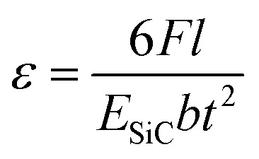 |
1 |
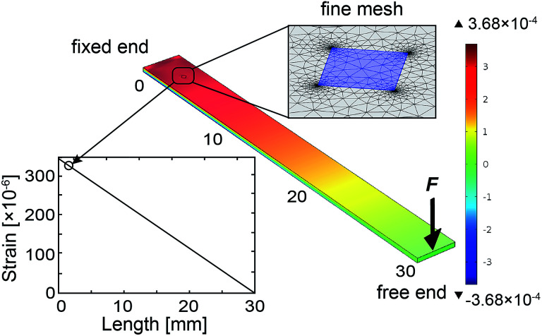
where l, b, t and ESiC are the length, width, thickness and Young's modulus of the 4H-SiC beam, respectively. The stress induced can be deduced from the Hooke's law: σ = εESiC.26 The calculation was in good agreement with a finite element analysis (FEA) model shown in Fig. 3.
Fig. 2. (a) Microscopic image of the 4HVP sensors aligned in three different orientations towards 〈11̄00〉 orientation. (b) Configuration of the experimental setup for the measurement of strain induced effect to the sensors. (c) The equivalent Wheatstone bridge circuit of the sensor.
Fig. 3. Strain distribution on the bending beam method by a FEA model with a linear strain gradient across the top surface of the 4H-SiC beam. The Young's modulus was obtained from ref. 22, with an applied force of 0.343 N, the strain induced to the device was obtained as 334 ppm.
Fig. 2(c) shows the configuration of the four-terminal strain sensor where the current was applied at the rectangular-shape-electrodes, while the output voltage was measured at the dot-shape-electrodes. According to the Kanda's model27,28 of a discrete constant circuit, the 4HVP sensor is a square-type Wheatstone bridge circuit comprised of four resistors RAC, RBC, RBD, and RAD. When a constant current is supplied between terminals A and B, in the stress-free state, all resistors are equal (RAC = RBC = RBD = RAD = R0) and the circuit is in its equilibrium, resulting in a null offset voltage (Voffset = 0) between the Hall terminals C and D. However, the resistances of the four resistors can vary differently depending on the orientation and magnitude of stress applied to each resistor since p-type 4H-SiC is a piezoresistive material. Upon the application of uniaxial stress in the 〈11̄00〉 orientation, there are asymmetric variations of the four piezoresistors, depending on the magnitude of stress and its relative direction versus the straining orientation. These different resistance changes yield a significant offset voltage between Hall terminals C and D (VCD). This phenomenon is referred to the pseudo-Hall effect in four-terminal devices where a large offset voltage can be generated without the application of an external magnetic field.27 Consequently, the four-terminal configuration can be employed as a strain sensor where the initial induced strain can be monitored by measuring the output voltage Vout = VCD. The relationship of the output signal Voutversus the four resistors is given by:16,17,27
 |
2 |
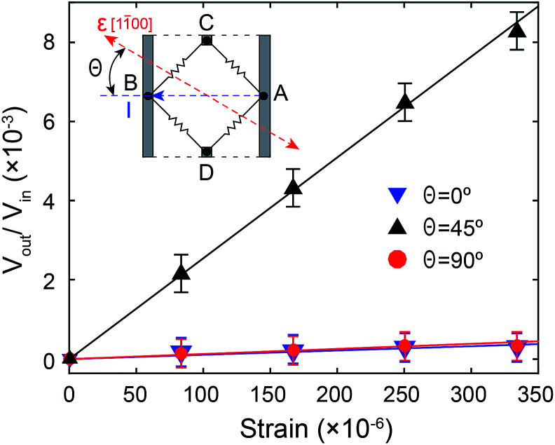
where Vin is the input voltage at the terminals A and B. The asymmetric variations of the four piezoresistors, in respect to the magnitude and orientation of applied stress, yields offset voltage Vout. The orientation dependence of the 4HVP sensor was characterized to obtain a high sensitivity. Fig. 4 shows the result of the offset voltage Vout in three different orientations aligned 0°, 45°, and 90° to 〈11̄00〉 direction with the supplied current of up to 30 μA. It can be seen that the output signals of the 0° and 90° aligned devices were almost zero. This can be explained by the symmetric changes of four piezoresistors in the 0° and 90° sensors regardless of the magnitude of induced strain. That is the resistances RAC/RBC changed with the same amount under a similar longitudinal strain, while the resistance of RBC and RAD almost changed equally under the same compressive strain. In contrast, a significant output voltage was obtained for the sensor with Θ = 45°.
Fig. 4. The relationship between the ratio of output voltage and input voltage versus applied uniaxial strain. The output voltage of the sensors with Θ = 45° was significant while the sensors with Θ = 0 or Θ = 90° resulted a nearly zero output signal (VCD ≈ 0).
This is attributed to the fact that RAC and RBD were elongated in their longitudinal direction parallel to the flowing current whereas RBC and RAD were stretched in transverse direction perpendicular to the current. Therefore, RAC/RBD and RBC/RAD vary with tensile stress followed the longitudinal GF (increase) and transverse GF (decrease), respectively.
The output voltage linearly varied with the applied strain ranging from 0 to 334 ppm (equivalent to an induced stress from 0 to 168 MPa), indicating that the Joule heating effect and the current leakage to the n-type layer and the substrate are negligible. Let Θ be the angle between the diagonal of the square-type circuit and the applied stress orientation (e.g. 〈11̄00〉) (Fig. 2(b)). Since the piezo-coefficients of p-type 4H-SiC have not been elucidated yet, there is no general formula, comprised of the four orientation-dependent piezoresistors, for the relationship between the ratio Vout/Vin and the sensor angle Θ. However, it is still possible to deduce for the case of Θ = 45° in which a uniaxial stress in 〈11̄00〉 orientation parallel to the diagonal axis of the 4HVP sensor. As such, RAC and RBD were elongated in their longitudinal direction parallel to the flowing current whereas RBC and RAD were stretched in transverse direction perpendicular to the current. Therefore, under the application of a uniaxial tensile strain, RAC and RBD vary by the longitudinal GF while the variation of RBC and RAD change by the transverse GF as follows:
 |
3 |
where GFL (positive value) and GFT (negative value) are longitudinal and transverse gauge factors of p-type 4H-SiC, which have been reported in ref. 22. From eqn (2) the sensitivity of the 4HVP sensor, for the case of Θ = 45°, is given by:
 |
4 |
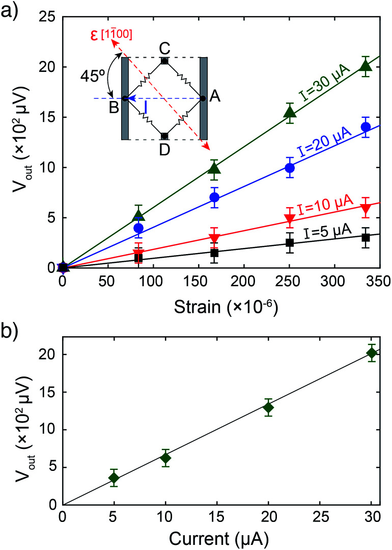
The experimental sensitivity of the sensor was found to be as high as 26.3 ppm−1 which are comparable with the theoretical result of 29.4 ppm−1 according to eqn (4). The measured sensitivity of 4HVP sensor is relatively high in comparison with other reported results of other SiC polytypes which were from 6 to 30.20 It should be noted that the sensitivity of the 4HVP sensor is independent of the applied current. Fig. 5(a) shows the relationship between the output voltage Voutversus the induced strain up to 334 ppm for the sensor with Θ = 45°. Evidently, the linear response of the sensor's signal was obtained with different applied currents ranging from 5 to 30 μA. At a certain strain, the output voltage of the sensor was proportional to the applied current as shown in Fig. 5(b). This characteristic is of interest for strain sensing since the sensor's calibration for different input currents is no longer required.
Fig. 5. (a) Output voltage of 4HVP sensor versus applied strains with different input currents of 5, 10, 20, and 30 μA. (b) Variation of output voltage versus varying applied current ranging from 5 to 30 μA at a constant strain of 334 ppm.
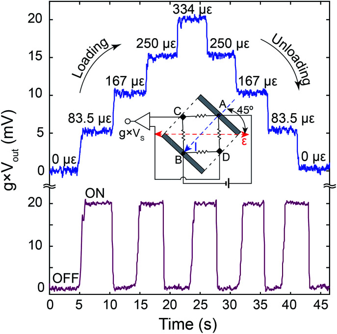
Fig. 6 shows a demonstration of the real-time strain monitoring using the 4HVP sensor. The operations under stepped strain and constant strain were carried out with the input current of 20 μA. The output signal amplitude can be amplified and monitored using a configuration shown in the inset of Fig. 6 with a gain g of the circuit to be adjustable. Under stepped strain, the sensor responded linearly with the increase or decrease of strain. The signal also remained stable at each strain level. When the load was completely removed, the sensor's output returned to its initial value. Additionally, with the application of a certain constant strain, the output was the application of a certain constant strain, the output was extremely stable without any signal drift. The measurement results indicate a good linearity and repeatability of the 4HVP strain sensor. This characteristic is of interest for high performance mechanical strain sensing with the high sensitivity and low signal-to-noise ratio.
Fig. 6. 4HVP sensor operation with stepped strains from 0 to 334 ppm (top) and at a constant applied strain of 334 ppm (I = 20 μA) (bottom). The Hall terminals C and D of the sensor were connected to an amplifier with a gain g. The excellent linearity and repeatability were obtained without any signal drift after numerous loading cycles.
Conclusions
A highly sensitive 4H-SiC van der Pauw strain sensor was presented using a four-terminal configuration which simplifies the read-out circuit without the need for the Wheatstone bridge to convert resistance change to voltage. By utilizing a bending beam method to apply uniaxial strain/stress to the sensor, a good repeatability and linearity were obtained for the sensor aligned 45° to the 〈11̄00〉 orientation. A high sensitivity of the strain sensor was found to be 26.3 ppm−1 and was independent of the applied current. The sensor is promising for highly sensitive and low noise mechanical sensing in high temperature operations.
Conflicts of interest
There are no conflicts to declare.
Supplementary Material
Acknowledgments
This work was partially funded by the linkage grants LP150100153 and LP160101553 from the Australian Research Council (ARC). This work was also supported by the Queensland node of the Australian National Fabrication Facility, a company established under the National Collaborative Research Infrastructure Strategy to provide nano and micro-fabrication facilities for Australia's researchers.
References
- Senesky D. G. Jamshidi B. Cheng K. B. Pisano A. IEEE Sens. J. 2009;9(11):1472–1478. doi: 10.1109/JSEN.2009.2026996. [DOI] [Google Scholar]
- Phan H.-P. Cheng H. H. Dinh T. Wood B. Nguyen T.-K. Mu F. Kamble H. Vadivelu R. Walker G. Hold L. Iacopi A. Haylock B. Dao D. V. Lobino M. Suga T. Nguyen N.-T. ACS Appl. Mater. Interfaces. 2017;9:27365–27371. doi: 10.1021/acsami.7b06661. [DOI] [PubMed] [Google Scholar]
- Phan H.-P. Dinh T. Kozeki T. Qamar A. Namazu T. Dimitrijev S. Nguyen N.-T. Dao D. V. Sci. Rep. 2016;6:28499. doi: 10.1038/srep28499. [DOI] [PMC free article] [PubMed] [Google Scholar]
- Okojie R. Lukco D. Nguyen V. Savrun E. IEEE Electron Device Lett. 2015;36(2):174–176. doi: 10.1109/LED.2014.2379262. [DOI] [Google Scholar]
- Phan H.-P. Nguyen T.-K. Dinh T. Ina G. Kermany A. R. Qamar A. Han J. Namazu T. Maeda R. Dao D. V. Nguyen N.-T. Appl. Phys. Lett. 2017;110:141906. doi: 10.1063/1.4979834. [DOI] [Google Scholar]
- Wijesundara M. B. J. and Azevedo R. G., Silicon carbide microsystems for harsh environments, Springer, 2011 [Google Scholar]
- Akiyama T. Briand D. de Rooij N. F. J. Micromech. Microeng. 2012;22(8):085034. doi: 10.1088/0960-1317/22/8/085034. [DOI] [Google Scholar]
- Zhang N. Lin C.-M. Senesky D. G. Pisano A. P. Appl. Phys. Lett. 2014;104(7):073504. doi: 10.1063/1.4865372. [DOI] [Google Scholar]
- Vandelli N. MicroNano News. 2008:10–12. [Google Scholar]
- Dinh T. Phan H.-P. Kozeki T. Qamar A. Fujii T. Namazu T. Nguyen N.-T. Mater. Lett. 2016;177:80–84. doi: 10.1016/j.matlet.2016.04.171. [DOI] [Google Scholar]
- Phan H.-P. Dinh T. Kozeki T. Nguyen T.-K. Qamar A. Namazu T. Nguyen N.-T. Dao D. V. Appl. Phys. Lett. 2016;109(12):123502. doi: 10.1063/1.4963258. [DOI] [Google Scholar]
- Bi J. Wei G. Wang L. Gao F. Zheng J. Tang B. Yang W. J. Mater. Chem. C. 2013;1(30):4514–4517. doi: 10.1039/C3TC30655K. [DOI] [Google Scholar]
- Gao F. Zheng J. Wang M. Wei G. Yang W. Chem. Commun. 2011;47:11993–11995. doi: 10.1039/C1CC14343C. [DOI] [PubMed] [Google Scholar]
- Li X. Chen S. Ying P. Gao F. Liu Q. Shang M. Yang W. J. Mater. Chem. C. 2016;4:6466–6472. doi: 10.1039/C6TC01882C. [DOI] [Google Scholar]
- Mian A. Suhling J. C. Jaeger R. IEEE Sens. J. 2006;6:340–356. doi: 10.1109/JSEN.2006.870140. [DOI] [Google Scholar]
- Qamar A. Phan H.-P. Han J. Tanner P. Dinh T. Wang L. Dao D. V. Dimitrijev S. J. Mater. Chem. C. 2015;34(3):8804–8809. doi: 10.1039/C5TC01898F. [DOI] [Google Scholar]
- Qamar A. Phan H.-P. Dao D. Tanner P. Dinh T. Wang L. Dimitrijev S. IEEE Electron Device Lett. 2015;36(7):708–710. doi: 10.1109/LED.2015.2435153. [DOI] [Google Scholar]
- Phan H. P. Qamar A. Dao D. V. Dinh T. Wang L. Han J. Nguyen N. T. RSC Adv. 2015;5:56377–56381. doi: 10.1039/C5RA10144A. [DOI] [Google Scholar]
- Qamar A. Dao D. V. Han J. Iacopi A. Dinh T. Phan H.-P. Dimitrijev S. Key Eng. Mater. 2017;733:3–7. doi: 10.4028/www.scientific.net/KEM.733.3. [DOI] [Google Scholar]
- Qamar A. Dao D. V. Han J. Phan H.-P. Younis A. Tanner P. Dinh T. Wang L. Dimitrijev S. J. Mater. Chem. C. 2016;3:12394. doi: 10.1039/C5TC02984H. [DOI] [Google Scholar]
- Qamar A. Dinh T. Jafari M. Iacopi A. Dimitrijev S. Dao D. V. Mater. Lett. 2017;213:11–14. doi: 10.1016/j.matlet.2017.10.117. [DOI] [Google Scholar]
- Nguyen T.-K. Phan H.-P. Dinh T. Han J. Dimitrijev S. Tanner P. Md Foisal A. R. Zhu Y. Nguyen N. T. Dao D. V. IEEE Electron Device Lett. 2017;38(7):955–958. doi: 10.1109/LED.2017.2700402. [DOI] [Google Scholar]
- Akiyama T. Briand D. de Rooij N. F. Proc. IEEE Sens. 2011:222–225. [Google Scholar]
- Okojie R. S. Ned A. A. Kurtz A. D. Carr W. N. IEEE Trans. Electron Devices. 1998;45(4):785–790. doi: 10.1109/16.662776. [DOI] [Google Scholar]
- Shor J. Bemis L. Kurtz A. IEEE Trans. Electron Devices. 1994;41(5):661–665. doi: 10.1109/16.285013. [DOI] [Google Scholar]
- Dao D. V. Phan H.-P. Qamar A. Dinh T. RSC Adv. 2016;6(26):21302–21307. doi: 10.1039/C5RA28164D. [DOI] [Google Scholar]
- Kanda Y. Yasukawa A. Sens. Actuators. 1982;2(3):283–296. [Google Scholar]
- Kanda Y. Yamamura K. Sens. Actuators. 1989;18(3):247–257. doi: 10.1016/0250-6874(89)87032-5. [DOI] [Google Scholar]


