Abstract
Lead sulfide (PbS) quantum dots (QDs) have been incorporated into PTB7:PC71BM BHJ active layers to fabricate polymer solar cells (PSCs) and gather on the top surface of active layers to form an ultrathin interlayer. The PbS QDs ultrathin interlayer with an appropriate thickness increases the carrier transport capacity, exciton dissociation and reduces the carrier recombination, which leads to a higher short circuit current (Jsc) and fill factor (FF). Finally, the power conversion efficiency (PCE) improves from 7.03% (control devices) to 7.87% with an ultrathin interlayer by doping 5% PbS QDs, while the current density (Jsc) and fill factor (FF) enhances from 13.83 mA cm−2 to 14.81 mA cm−2 and from 68.70% to 70.85%, respectively.
Lead sulfide (PbS) quantum dots (QDs) have been incorporated into PTB7:PC71BM BHJ active layers to fabricate polymer solar cells (PSCs) and gather on the top surface of active layers to form an ultrathin interlayer.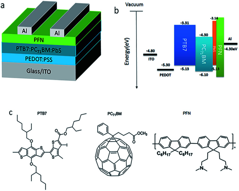
Introduction
Polymer solar cells (PSCs) have advantages such as low-cost, light weight, flexibility and easy fabrication via printing and roll-to-roll coating technologies, and are being widely investigated as an alternative energy source.1–5 Although the power conversion efficiency (PCE) of PSCs has reached 14% in the state of the art,6 there is an urgent need to enhance the short-circuit current density (Jsc),7 open-circuit voltage (Voc),8,9 fill factor (FF)10 and PCE for mass production and practical applications. There are many approaches to improve the performance of PSCs such as developing new low bandgap donor materials,11,12 incorporation of an additive into the active layer,13 tandem cell approach14 and so on. In these PSCs, the charge transport at each interface of different layers is critical for enhancing the efficiency, thus interfacial engineering plays an important role to optimize the photovoltaic characteristics by increasing the charge extraction and weakening the charge recombination.15 Methods of the interfacial modification in PSCs have been reported such as using different interlayers,16 polar solvent dispose17 and so on. Alcohol-/water-soluble polymers are ideal to be used as the interfacial layer in PSCs to avoid the dissolving of two layers, which successfully improved device performance as a dipole layer to increase the charge extraction.18 PFN is one of alcohol-/water-soluble polymers and frequently be used as the interfacial material in PSCs. The morphology of this polymer dipole layer is easy to be effected by the hydrophobic surface of the previous layer. Thus, it's necessary to modify the interface between the active layer and the polymer dipole layer by using an easy fabrication process, which could improve the electron transfer from the active layer to the polymer dipole layer and result in an optimized photovoltaic performance.
Quantum dots (QDs) materials have advantages such as a broad absorption range, high absorption coefficient, high conductivity and high carrier mobility.19–21 In addition, the conduction band and the valence band of QDs material can be adjusted via controlling its size for different application. Furthermore, QDs are dispersed and stabilized in solvent by the introduction of ligands, which leads to the solution process available.22 These characteristics make suitable QDs own the potential to enhance the performance of PSCs as additives, or as the electron accepter. Lee23et al. introduced PbS QDs with different bandgap energy (0.9–1.7 eV) instead of [6,6]-phenyl-C71-butyric-acid methyl-ester (PC71MB) as an electron acceptor with poly[2,6-(4,40-bis(2-ethylhexyl)dithieno[3,2-b:20,30-d]silole)-alt-4,7(2,1,3-benzothiadiazole)] (PSBTBT) as the polymer donor, and got a PCE of 3.48%. Guo24et al. reported a PCE of 6.94% by introducing the cadmium selenide (CdSe) QDs as an additive into the blend of poly [N-900-hepta-decanyl-2,7-carbazole-alt-5,5-(40,70-di-2-thienyl-20,10,30-ben-zothiadiazole)] (PCDTBT) and the fullerene derivative PC71BM. The improvements of the photovoltaic performance were explained by improving the charge transport property and tuning the energy levels after introducing the QDs. In addition to these applications, QDs could act as an interlayer to modify the interface of PSCs due to their adjusted energy levels to improve the photovoltaic performance. However, there is no any such reports according to out knowledge.
In this work, we achieved positive effects arising from the addition of PbS QDs into the blend of poly[[4,8-bis[(2-ethylhexyl)oxy]benzo[1,2-b:4,5-b′]dithiophene-2,6-diyl][3-fluoro-2-[(2-ethylhexyl)carbonyl]thieno[3,4-b]thiophenediyl]] (PTB7) and fullerene derivative [6,6]-phenyl-C71-butyric acid methyl ester (PC71BM). An ultrathin PbS QDs film as an interlayer between the active layer and the polymer interfacial layer is formed to boost the transport of electrons by a new and easier experiment process. The thickness and the morphology of the ultrathin PbS QDs film were optimized with various weight ratios (wt). Then the carrier transport capacity and the exciton dissociation was investigated. The results show that Jsc and FF, then the photovoltaic performance of prepared PTB7:PC71BM photovoltaics devices are enhanced.
Experimental
The lead sulfide (PbS) QDs was purchased from Mesolight Inc., PC71BM, PTB7 and PFN were commercially procured from 1-martial Inc. and used as received. The devices 1–6 were fabricated with the structure: ITO/PEDOT:PSS/PTB7:PC71BM:PbS QDs (x wt%)/PFN/Al, which was shown in Fig. 1a. The devices 7 were fabricated with the ITO/PEDOT:PSS/PTB7:PC71BM/PbS QDs/PFN/Al shown in Fig. S2†
Fig. 1. (a) Schematic image of polymer BHJ solar cells device structure, (b) the energy diagram of solar cells, (c) materials chart, including the polymer donor PTB7, PC71BM as the fullerene acceptor, and the conjugated polyelectrolyte PFN.
The blend solution of PTB7:PC71BM:PbS QDs was prepared as follows: PTB7 and PC71BM with the weight ratio of 3 : 2 were dissolved in chlorobenzene (polyphenyl ether (DPE) 3 vol%) with overall concentration of 20 mg ml−1, simultaneously, PbS QDs was dissolved in chlorobenzene with the concentration of 10 mg ml−1 and the two solution were stirred at 25 °C in a N2 glovebox for 12 h. Then the PTB7:PC71BM and PbS QDs solutions were blended to make PTB7:PbS QDs:PC71BM solution where the weight ratios of PbS QDs and PTB7:PC71BM blend was 0, 1%, 3%, 5%, 7% and 10% respectively corresponding to device 1, 2, 3, 4, 5 and 6.
The devices were prepared on glass/ITO substrates. Firstly, indium tin oxide (ITO) coated glass substrates (sheet resistance of 15 ohm per square) were cleaned in an ultrasonic bath with detergent solution deionized water, acetone, ethanol successively for 30 min, and then immediately blow-dried by high density nitrogen, followed by UV processing for 6 min. A highly conducting polymer PEDOT:PSS was spin coated onto the treated ITO substrates from an aqueous solution at 5000 rpm for 30 s, then these ITO coated with PEDOT:PSS were annealed at 150 °C for 10 min. Then, the active layer, PTB7:PC71BM as a reference (devices 1 and devices 7) and PTB7:PbS QDs:PC71BM (with different PbS QDs weight ratio) were prepared through spin coating at 1000 rpm for 90 s in N2-filling glove box. Then the wet films thoroughly dried in vacuum chamber for 1 hour. For devices 7, the PbS QDs(5 mg ml−1 in octane) was spin coated before PFN electron transport layer at 4000 rpm for 50 s. Then PFN electron transport layer was spin-coated on the active layer at 3000 rpm for 50 s. Finally, Al cathodes (with the film thickness of 1000 Å) were deposited on the top at rate of 1.5 Å s−1 under a vacuum pressure of 2 × 10⁻⁴ Pa. The active area of solar cells is 4 mm2.
The J–V characteristic curves of solar cells were measured with a Keithley 4200 source equipment unit under AM 1.5 G simulated solar illumination with an intensity of 100 mW cm−2. The EQE measurements were performed using a QE/IPCE Measurements Solar Cell Scan 100 (ZOLIX) system equipped with calibrated silicon photodiode as the reference cell. The UV-Vis absorption spectrum was acquired on Shimadzu UV-3101 PC spectrometer. The surface morphology characteristics and 3D images was measured by atomic force measurement(AFM, PSIA XE-100). The transmission electron microscope (TEM) images were obtained by using a high-resolution transmission electron microscope (HR-TEM, JEM-2100) operating at 200 kV. Prior to the TEM characterization, the films were stripped from PEDOT:PSS substrate by soaking the samples into deionized water and then transfer onto a holey carbon coated copper grid. For the time-resolved PL measurements, the samples were excited using a 450 nm pulsed laser; the dynamic signal was recorded using a time-correlated single photon counting (TCSPC) spectrometer. The PL decay data are fitted using a double exponential function of the form:
| I(t) = I1e−t/τ1 + I2e−t/τ2 | 1 |
where I1,2 are the amplitudes of the decay, and τ1,2 are the corresponding exponential constants. The contribution of each of the two time constants is quantified by its relative amplitude, A1,2, expressed as:
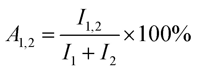 |
2 |
The effective exciton lifetime is defined in the blends as τexc = A1τ1 + A2τ2.25
The secondary ion mass spectrum was obtained using a time-of-flight secondary ion mass spectrometer TOF-SIMS 5-100 from ION-TOF GmbH (Munster, Germany). For all of the depth profile measurements, a gas cluster ion gun O2+ operating at a 1 keV beam voltage with a 45° incident angle was used for sputter erosion, and the sputtering rate was 0.263 nm s−1 for SiO2. Analysis was performed using a Bi1+ liquid metal ion gun operated at 30 keV beam voltage with a 45° incident angle over a 100 μm × 100 μm2 region in the center of the eroded area. A low energy electron flood gun was carried out for charge compensation.
Results and discussion
The device structure and the highest occupied molecular orbital (HOMO), lowest unoccupied molecular orbital (LUMO), valence band and conduction band of component materials used in devices are shown in Fig. 1a and b, respectively. The energy band diagram of PbS QDs was measured by ultraviolet photoelectron spectroscopy(UPS).26 The molecular structures of the organic polymer donor PTB7, fullerene acceptor PC71BM that used as the photoactive layer and water/alcohol soluble conjugated polymer poly[(9,9-bis(30-(N,N-dimethylamino)-propyl)-2,7-fluorene)-alt-2,7-(9,9-dioctylfluorene)] PFN that used as the interlayer material are shown in Fig. 1c.
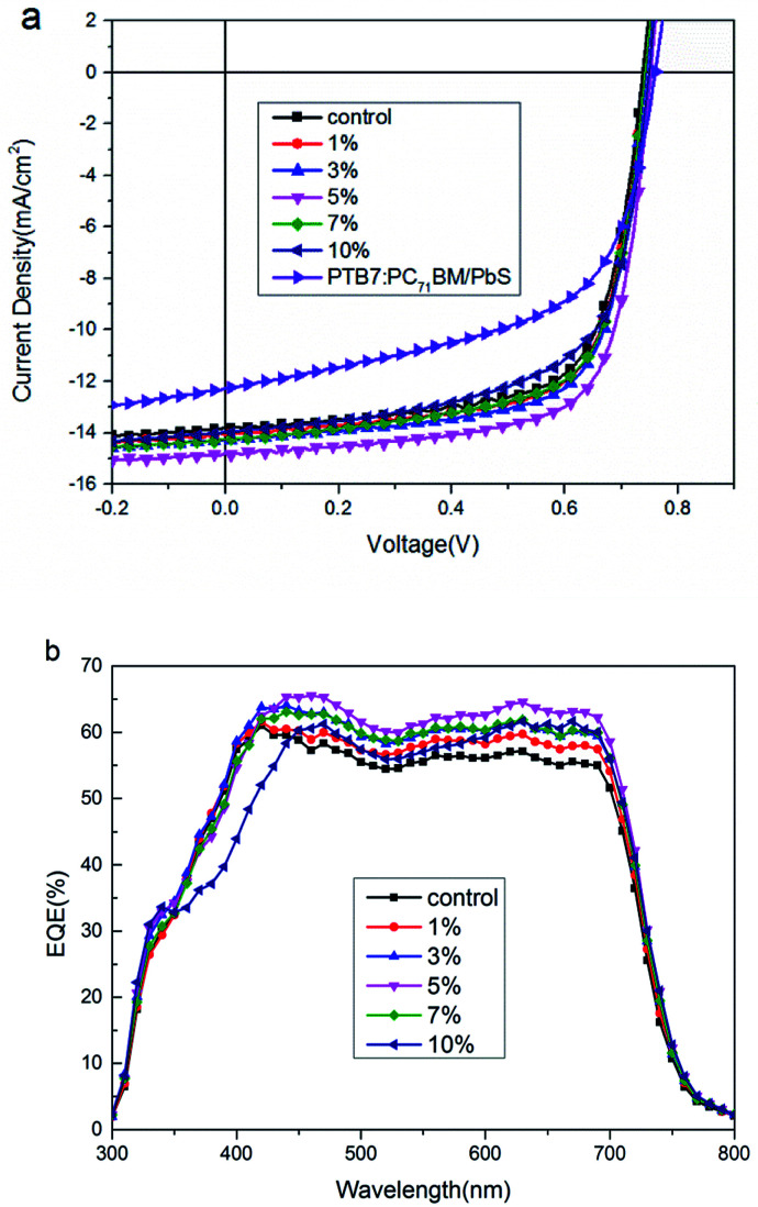
Fig. 2 shows the J–V characteristics of devices with different doping amounts of PbS QDs under AM1.5G illumination with the intensity of 100 mW cm−2. The control devices without PbS QDs exhibit a Jsc of 13.83 mA cm−2, Voc of 0.74 V and FF of 68.70%, which results in a PCE of 7.03%. As expected, the performance of the devices doped PbS QDs was improved dramatically. The cells with an optimum ratio of 5% doped has a PCE of 7.87%, with a Jsc of 14.81 mA cm−2, a Voc of 0.75 V and a FF of 70.85%, which directly leads to an enhancement of PCE with 13% higher than that of control devices. Besides, the shunt resistance (Rsh) of device increases from 589.42 Ω cm2 (contrast devices) to 1043.96 Ω cm2 after doping 5% PbS QDs. The larger Rsh indicates a lower charge carrier recombination in the active layer. This implies that doping PbS QDs can effectively restrain the leakage current under reverse bias, which could provide the effective charge carrier transport in the blend layers, and result in the increase of Jsc compared with the control devices.27,28 However, We can also find that 10% doping devices produced a negative effect, with a Jsc of 13.96 mA cm−2 and the FF decreased significantly from 68.70% to 64.02%, leading to a PCE of 6.70%. It indicates that the excess doping will damage the photovoltaic property.
Fig. 2. (a) The J–V characteristics of devices doping with various amounts of PbS QDs (0, 1%, 3%, 5%, 7%, 10%) and with structure of ITO/PEDOT:PSS/PTB7:PCBM/PbS/PFN/Al under AM1.5G illumination. (b) EQE versus wavelength of devices with various amounts of PbS QDs.
For comparison, a PbS quantum dots layer is deposited between active layer and PFN layer, which exhibits a low PCE of 5.41% with poor Jsc, Voc and FF. It demonstrates QDs layer by itself has negative effect to devices. The detailed data of all devices performance are summarized in Table 1.
Summary of solar cell parameters at the structure of ITO/PEDOT:PSS/PTB7:PC71BM:PbS QDs (x wt%)/PFN/Al and ITO/PEDOT:PSS/PTB7:PC71BM/PbS QDs/PFN/Al.
| Device | PCE (%) | J sc (mA cm−2) | V oc (V) | FF (%) |
|---|---|---|---|---|
| Control | 7.03 | 13.83 | 0.74 | 68.70 |
| 1% PbS doped | 7.21 | 14.08 | 0.74 | 69.20 |
| 3% PbS doped | 7.36 | 14.29 | 0.74 | 69.59 |
| 5% PbS doped | 7.87 | 14.81 | 0.75 | 70.85 |
| 7% PbS doped | 7.20 | 14.27 | 0.74 | 68.20 |
| 10% PbS doped | 6.70 | 13.96 | 0.75 | 64.02 |
| Active layer/PbS | 5.41 | 12.30 | 0.76 | 57.89 |
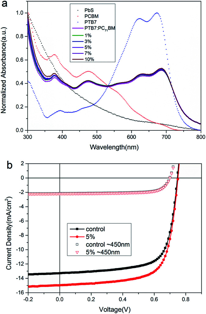
The external quantum efficiency (EQE) measurements were performed as shown in Fig. 2b. The two energy peaks in the region between 300 nm to 500 nm correspond to the absorption of PC71BM. The third and forth energy peaks between 600 nm and 700 nm are attributed to the absorption of PTB7. The absorption peak onset of the PbS QDs is found at λ = 650 nm (shown in Fig. 3a) and the bandgap energy of QDs is 1.99 eV (shown in Fig. 1b). The UV-Vis absorption spectra of PTB7:PbS QDs (x wt%): PC71BM blend in Fig. 3a show a similar absorption spectra of the PTB7:PC71BM blend except the absorption slightly increases over the whole wavelength region after doping the PbS QDs and becomes higher with increasing the doping ratio. Compared with the absorption spectra, the EQE value is noticeably enhanced over the whole wavelength region when the incorporation ratio of PbS QDs is 5%.
Fig. 3. (a) UV-Vis absorption spectra of PbS QDs, PC71BM, PTB7 and PTB7: PC71BM blend film various amounts of PbS QDs doped, (b) the J–V characteristics of devices doping without and with 5 wt% PbS QDs over wavelength below 450 nm (symbols) and the whole region (line and symbols).
Therefore, it is concluded that this improvement is not due to the film absorption enhancement because that the absorption spectrum (shown as Fig. 3a) is not sensitive to the increase ratio of PbS QDs. It means that PbS QDs doping does not help to form more excitons but help to dissociate excitons or transport charges.
In order to investigate the physical mechanism of PbS QDs in devices, we measured J–V characteristics of devices without and with 5% PbS QDs under the illumination of a monochromatic light at 450 nm, which is shown in Fig. 3b. According to the UV-Vis absorption spectra of PbS QDs and PTB7, it's obvious that the absorption intensity of PTB7 is weak below 450 nm while PbS QDs has strong absorbance. However, the J–V curves are almost same for two devices under 450 nm illumination. It also indicate that the photons absorbed by PbS QDs can not be transferred to free carriers, and there is not Förster energy transfer between PbS QDs to PTB7.
In other words, the light absorbed by PbS QDs does not contribute to the enhancement of PCE.
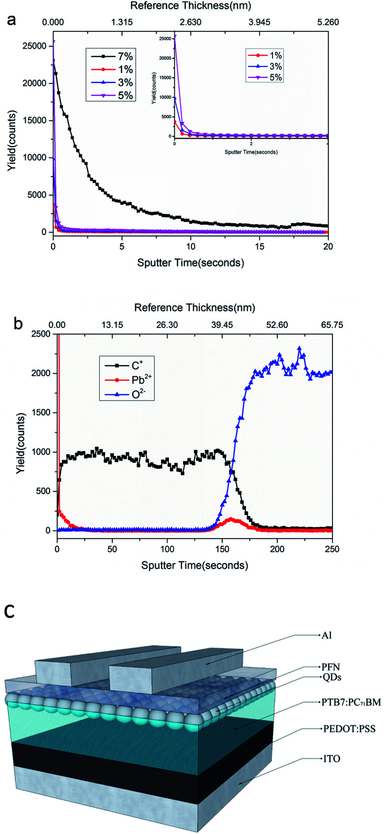
The location and distribution of PbS QDs in the active layer is very important to play its role to enhance the whole device performance. Time of Flight Secondary Ion Mass Spectrometry (ToF-SIMS) was utilized to figure out the distribution of PbS QDs and PTB7 by measuring the yield of lead ion and fluorine (Pb2+ and C+). The ToF-SIMS results in the vertical direction of films with different amounts of PbS QDs are shown in Fig. 4. In Fig. 4a, the intensity of Pb2+ in the film surface corresponding to the beginning of the sputter time enhances with the increasing doping amounts of PbS QDs till the doping over 5%, which indicates that PbS QDs cover the surface of film completely when the doping amounts is 5% and 7%, and covers partially when it's 1% and 3%. Furthermore, the intensity of Pb2+ in films with lower doping than 5% reaches zero rapidly in less than 2 seconds (which is clearly shown in the inset figure) while the decreasing rate of intensity is much slower with doping 7% PbS QDs. This phenomenon proves that during the film formation, PbS QDs prefer to move upward to form an ultrathin layer in the surface. When the surface of the films is overspreaded by PbS QDs, partial PbS QDs migrate or diffuse into the inside of BHJ films. Therefore, the thickness of PbS QDs layer with 7% doped is larger than that of the layer doped with 5%. To related with the photovoltaic performance of different devices, we can make a reasonable conclusion that the ultrathin PbS QDs layer could promote the carrier transport or charge extraction, yet a thick PbS QDs layer has an adverse effect to organic solar cells.
Fig. 4. ToF-SIMS depth profile for: (a) Pb2+ in film doping with different amounts of PbS QDs within 5 nm, (b) Pb2+, C+ and O2− in whole film with 5% PbS QDs. The inset figure is an amplification of local curves of the film with 1%, 3%, 5% PbS QDs doped. The top horizontal axis respect the reference thickness at sputter rate is 0.263 nm s−1 for SiO2. (c) Structure of devices with doping 5% PbS QDs.
To confirm that PbS QDs gathers on the top of films,29,30 yield of lead ion, carbon ion and oxygen ion were measured respectively in the whole film with doping 5% PbS QDs as shown in Fig. 4b. Pb2+ represents PbS QDs, C is the fragment element associated with PTB7 molecule, and O2− is main associated with ITO (due to its little content in PTB7). At the beginning, in which it corresponds to the surface of the BHJ layer, the yield intensity of Pb2+ is more than other two ions. After 2 second and till 148 second, the intensity of Pb2+ is almost zero. It indicates PbS QDs locating on the top surface, and there is not PbS QDs existing inside the BHJ layer. After the yield intensity of O2− rapidly rises to show the bottom of the active layer and the surface of ITO arrived. Then a very little Pb2+ still was detected in the bottom of the film and could be neglected compared with the surface Pb2+ yield. According to above results, PbS QDs gather on the top of the active layer, we conjecture that PbS QDs would float upward during spinning progress due to the less molar mass of PbS QDs than that of PTB7 and PC71BM. It has a new structure of device with 5% doping PbS QDs, shown in Fig. 4c, which could get the maximum improvement of device performance.
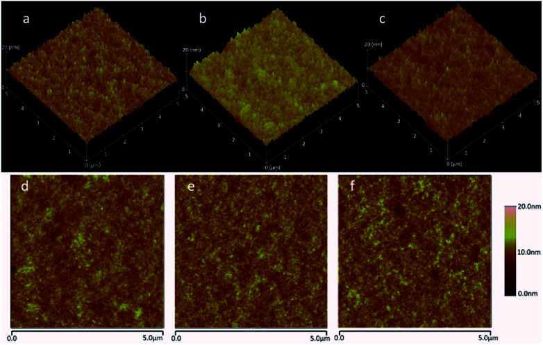
The morphology of this PbS QDs layer are presented by tapping-mode atomic force microscopy (AFM) images (surface area: 5 × 5 μm2) of films with 0, 5%, and 10% PbS QDs in Fig. 5. As we can see, the blend films don't exhibit apparent variation upon doping 5% PbS QDs (Fig. 5b and e) and 10% PbS QDs (Fig. 5c and f). The blend film with 5% PbS QDs doped shows a rather smooth surface morphology with root mean square (RMS) values of about 1.195 nm. In contrast, the blend film without PbS QDs doped (Fig. 5a) and with 10% PbS QDs doped (Fig. 5c) show rough morphology with RMS values of about 1.381 nm and 1.509 nm respectively, which is similar with the FF of devices. The rather smooth surface is conducive to the interface contact between layers and reduces the interface resistance to promote the charge transport and extraction.
Fig. 5. AFM image of PTB7:PC71BM blend film (a and d) without PbS QDs, (b and e) doping with 5% QDs, (c and f) doping with 10% QDs.
It also can be proved by transmission electron microscopy (shown in Fig. S1†). The black domain is assigned as the PC71BM aggregation because its ordered aggregation shows relatively higher electron scattering density compared to the amorphous polymer aggregation.31 The blend film with 5% PbS QDs doped exhibits rather compact bulk morphology which indicates the PC71BM aggregation decreases and homogeneous dispersion throughout the film. It is benefit to form better interpenetrating network structure in the bulk to promote the charge transport.
These phenomena indicate that PbS QDs ultrathin layer with appropriate thickness are favorable to charge transport and extraction in the active layer, to improve the photovoltaic performance.
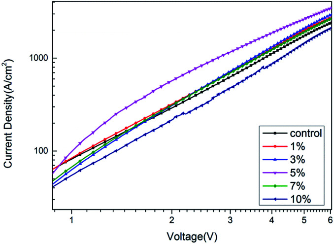
The dark J–V characteristics of electron-only devices were measured with the structure of ITO/active layer/PFN/Al shown in Fig. 6. Jsc of doped devices with lower contents in Fig. 6 is larger than that of control device it means that PbS QDs ultrathin layer is benefit to enhance the electron transport property. As the same time, a largest Jsc was detected in the device with the doping amount of 5%, which is consistent with the tendency of the photocurrent curves in Fig. 2. It implies that an ultrathin QDs layer formed by doping 5% QDs is maximally benefit to charge transport. Then we made a realistic evaluation on the apparent charge carrier mobility of blend films through the spare charge limit current (SCLC) method.18,25,32,33 According to the Mott–Gurney law, current density is given by (eqn (3))
| J = 9ε0εrμV2/8L3 | 3 |
where J is the current density, ε0 is the permittivity of free space, εr is the relative dielectric constant of the BHJ layer, μ is the charge carrier mobility, L is the thickness of the BHJ layer, and V is the voltage drop across the device.34 The computed results show that the electron-mobility μe increases from 9.58 × 10⁻⁵ cm2 V−1 s−1 to 6.90 × 10⁻⁴ cm2 V−1 s−1 with an ultrathin QDs layer formed by doping 5% QDs. That is to say, upon the PbS QDs ultrathin layer, the electron mobility increase 7.2 times. Those are direct evidence that charge transport capacity is largely enhanced by PbS QDs ultrathin layer and contributes to improvement of Jsc, FF as well as the performance of the solar cells.
Fig. 6. Dark J–V characteristics of electron-only devices with various amounts of PbS QDs doping (1%, 3%, 5%, 7%, 10%), for the calculation of electron mobility using the Mott–Gurney equation.
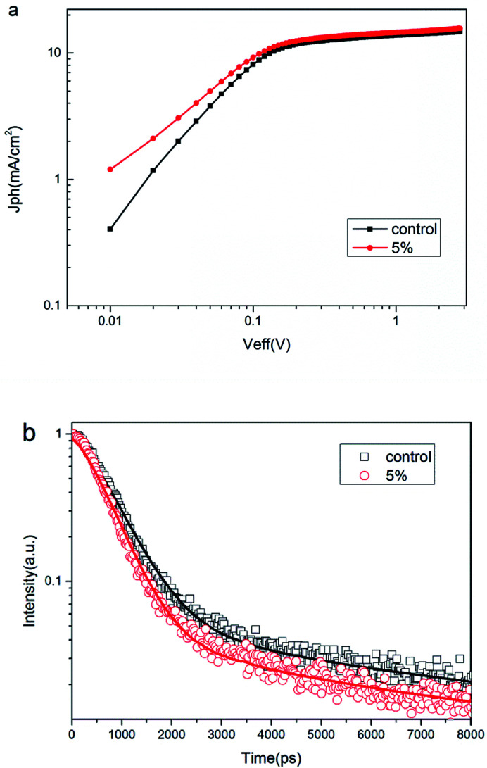
In order to investigate the origin of the enhancement in Jsc and FF for the PSCs without and with PbS QDs ultrathin layer, we measured the photocurrent density (Jph) versus the effective voltage (Veff) curves for the devices doping without and with 5% PbS QDs. The curve of Jphversus Veff is plotted in Fig. 7. In principle, Jph is calculated according to
| Jph = JL − JD | 4 |
where JL and JD represent current density under AM1.5G illumination and in the dark, respectively. Veff is calculated according to
| Veff = V0 − Va | 5 |
where V0 stands for the voltage at which Jph = 0 and Va is the applied voltage. We can find that the Jph of both solar cells shows linear dependence on the voltage at a low Veff (<0.1 V), and rapidly reaches saturation at the high Veff (>1 V). It clearly shows that the devices with PbS QDs ultrathin layer has a higher saturation photocurrent density (Jsat) than that of contrast devices. The charge dissociation probability P(E,T) of both devices determined by Jph/Jsat under short circuit condition are 86.71 and 91.86%, respectively, indicating that the PbS QDs ultrathin layer appropriately facilitated excitons to dissociate into free carriers.
Fig. 7. (a) Photocurrent density (Jph) versus effective voltage (Veff) for the solar cells doping with 0 wt% and 5 wt% PbS QDs, (b) time-resolved photoluminescence spectra of PTB7:PC71BM blend film with 0 wt% and 5 wt% PbS QDs, the emission at 750 nm was recorded after excitation at 450 nm.
Time-resolved transient photoluminescence (TRTPL) spectra25,35 of the blend PTB7:PC71BM with and without PbS QDs ultrathin layer probed at 750 nm under the excitation of 450 nm pulse laser source is shown in Fig. 7b, which shows that the film with the ultrathin PbS QDs layer has a shorter exciton lifetime. It means that excitons in this device should be dissociated faster and then mobile charges are extracted faster in the active layer. The boosted charge transfer rate favors the collection of electrons on the electrode and consequently increases Jsc of solar devices.
Conclusions
In summary, utilizing PbS QDs incorporating into polymer solar cells composed of PTB7 and PC71BM to form an ultrathin layer enhanced the Jsc and FF, which resulted in a PCE up to 7.87%. The performance improvement of polymer solar cells is attributed to the enhancement of the charge carrier transport property and exciton dissociation as well as reduction of the carrier recombination by controlling the morphology of the active layer. The performance of PSCs can be increased by quantum dots ultrathin layer modifying, which has a far reaching impact on the industrialization of PSCs because of the effortless fabrication process.
Conflicts of interest
There are no conflicts to declare.
Supplementary Material
Acknowledgments
The authors express the thanks to the National Natural Science Foundation of China under Grant No. 61575019 and 61775013 and the Fundamental Research Funds for the Central Universities with the Grant No. 2017RC015.
Electronic supplementary information (ESI) available. See DOI: 10.1039/c8ra02770f
Notes and references
- Kim J. Y. Kim S. H. Lee H. H. Lee K. Ma W. Gong X. Heeger A. J. Adv. Mater. 2006;18:572–576. doi: 10.1002/adma.200501825. [DOI] [Google Scholar]
- Zang H. Liang Y. Yu L. Hu B. Adv. Energy Mater. 2011;1:923–929. doi: 10.1002/aenm.201100304. [DOI] [Google Scholar]
- Krebs F. C. Gevorgyan S. A. Alstrup J. J. Mater. Chem. 2009;19:5442. doi: 10.1039/B823001C. [DOI] [Google Scholar]
- Chen C. P. Chen Y. D. Chuang S. C. Adv. Mater. 2011;23:3859–3863. doi: 10.1002/adma.201102142. [DOI] [PubMed] [Google Scholar]
- Wang D. H. Moon J. S. Seifter J. Jo J. Park J. H. Park O. O. Heeger A. J. Nano Lett. 2011;11:3163–3168. doi: 10.1021/nl202320r. [DOI] [PubMed] [Google Scholar]
- Xiao Z. Jia X. Ding L. Sci. Bull. 2017;62(23):562–1564. doi: 10.1016/j.scib.2017.11.003. [DOI] [PubMed] [Google Scholar]
- Inganäs O. Zhang F. Tvingstedt K. Andersson L. M. Hellström S. Andersson M. R. Adv. Mater. 2010;22:E100–E116. doi: 10.1002/adma.200904407. [DOI] [PubMed] [Google Scholar]
- Brabec C. J. Cravino A. Meissner D. Sariciftci N. S. Fromherz T. Rispens M. T. Sanchez L. Hummelen J. C. Adv. Funct. Mater. 2010;11:374–380. doi: 10.1002/1616-3028(200110)11:5<374::AID-ADFM374>3.0.CO;2-W. [DOI] [Google Scholar]
- Zhao G. He Y. Li Y. Adv. Mater. 2010;22:4355–4358. doi: 10.1002/adma.201001339. [DOI] [PubMed] [Google Scholar]
- Mandoc M. M. Veurman W. Koster L. J. A. De Boer B. Blom P. W. M. Adv. Funct. Mater. 2010;17:2167–2173. doi: 10.1002/adfm.200601110. [DOI] [Google Scholar]
- Wang E. Wang L. Lan L. Luo C. Zhuang W. Peng J. Cao Y. Appl. Phys. Lett. 2008;92:033307. doi: 10.1063/1.2836266. [DOI] [Google Scholar]
- Wong W. Y. Wang X. Z. He Z. Djurisic A. B. Yip C. T. Cheung K. Y. Wang H. Mak C. S. Chan W. K. Nat. Mater. 2007;6:521–527. doi: 10.1038/nmat1909. [DOI] [PubMed] [Google Scholar]
- Peet J. Kim J. Y. Coates N. E. Ma W. L. Moses D. Heeger A. J. Bazan G. C. Nat. Mater. 2007;6:497–500. doi: 10.1038/nmat1928. [DOI] [PubMed] [Google Scholar]
- Jin Y. K. Lee K. Coates N. E. Moses D. Nguyen T. Q. Dante M. Heeger A. J. Science. 2007;317:222–225. doi: 10.1126/science.1141711. [DOI] [PubMed] [Google Scholar]
- Braun S. Salaneck W. R. Fahlman M. Adv. Mater. 2010;21:1450–1472. doi: 10.1002/adma.200802893. [DOI] [Google Scholar]
- Yip H. L. Hau S. K. Baek N. S. Ma H. Jen K. Y. Adv. Mater. 2010;20:2376–2382. doi: 10.1002/adma.200703050. [DOI] [Google Scholar]
- Tan Z. K. Vaynzof Y. Dan C. Li C. Casford M. T. L. Sepe A. Huettner S. Nikolka M. Paulus F. Yang L. Adv. Funct. Mater. 2014;24:3051–3058. doi: 10.1002/adfm.201303426. [DOI] [Google Scholar]
- He Z. Zhong C. Huang X. Wong W. Y. Wu H. Chen L. Su S. Cao Y. Adv. Mater. 2011;23:4636–4643. doi: 10.1002/adma.201103006. [DOI] [PubMed] [Google Scholar]
- Chopra K. L. Paulson P. D. Dutta V. Prog. Photovoltaics. 2004;12:69–92. [Google Scholar]
- Chander S. Dhaka M. S. Mater. Sci. Semicond. Process. 2015;40:708–712. doi: 10.1016/j.mssp.2015.07.063. [DOI] [Google Scholar]
- Cao X. Yamaguchi Y. Ninomiya Y. Yamada N. J. Appl. Phys. 2016;119:025104. doi: 10.1063/1.4939598. [DOI] [Google Scholar]
- Lan X. Z. Voznyy O. de Arquer F. P. G. Liu M. X. Xu J. X. Proppe A. H. Walters G. Fan F. J. Tan H. R. Liu M. Yang Z. Y. Hoogland S. Sargent E. H. Nano Lett. 2016;16:4630–4634. doi: 10.1021/acs.nanolett.6b01957. [DOI] [PubMed] [Google Scholar]
- Nam M. Park J. Kim S. W. Lee K. J. Mater. Chem. C. 2014;2:3978–3985. doi: 10.1039/C4TC01407C. [DOI] [Google Scholar]
- Liu C. Li J. Zhang X. He Y. Li Z. Li H. Guo W. Shen L. Ruan S. PCCP Phys. Chem. Chem. Phys. 2015;17:7960–7965. doi: 10.1039/C5CP00417A. [DOI] [PubMed] [Google Scholar]
- Kakavelakis G. Del Rio Castillo A. E. Pellegrini V. Ansaldo A. Tzourmpakis P. Brescia R. Prato M. Stratakis E. Kymakis E. Bonaccorso F. ACS Nano. 2017;11:3517–3531. doi: 10.1021/acsnano.7b00323. [DOI] [PubMed] [Google Scholar]
- Narioka S. Ishii H. Yoshimura D. Sei M. Ouchi Y. Seki K. Hasegawa S. Miyazaki T. Harima Y. Yamashita K. Appl. Phys. Lett. 1995;67:1899–1901. doi: 10.1063/1.114370. [DOI] [Google Scholar]
- Janssen R. A. Nelson J. Adv. Mater. 2013;25:1847–1858. doi: 10.1002/adma.201202873. [DOI] [PubMed] [Google Scholar]
- Huang D. Li Y. Xu Z. Zhao S. Zhao L. Zhao J. PCCP Phys. Chem. Chem. Phys. 2015;17:8053–8060. doi: 10.1039/C4CP05826G. [DOI] [PubMed] [Google Scholar]
- Han Y. W. Lee E. J. Joo J. Park J. Sung T. H. Moon D. K. J. Mater. Chem. C. 2016;4:10444–10453. [Google Scholar]
- Liu C. Li J. Zhang X. He Y. Li Z. Li H. Guo W. Shen L. Ruan S. Phys. Chem. Chem. Phys. 2015;17:7960–7965. doi: 10.1039/C5CP00417A. [DOI] [PubMed] [Google Scholar]
- Mao Z. Le T. P. Vakhshouri K. Fernando R. Ruan F. Muller E. Gomez E. D. Sauvé G. Org. Electron. 2014;15:3384–3391. doi: 10.1016/j.orgel.2014.09.021. [DOI] [Google Scholar]
- Azimi H. Senes A. Scharber M. C. Hingerl K. Brabec C. J. Adv. Energy Mater. 2011;1:1162–1168. doi: 10.1002/aenm.201100331. [DOI] [Google Scholar]
- Huang D. Li Y. Xu Z. Zhao S. Zhao L. Zhao J. Phys. Chem. Chem. Phys. 2015;17:8053–8060. doi: 10.1039/C4CP05826G. [DOI] [PubMed] [Google Scholar]
- Malliaras G. G. Brock P. J. Scott C. Salem J. R. Phys. Rev. B: Condens. Matter Mater. Phys. 1998;581:10371. [Google Scholar]
- Lee J. M. Lim J. Lee N. Park H. I. Lee K. E. Jeon T. Nam S. A. Kim J. Shin J. Kim S. O. Adv. Mater. 2015;27:1519–1525. doi: 10.1002/adma.201404248. [DOI] [PubMed] [Google Scholar]
Associated Data
This section collects any data citations, data availability statements, or supplementary materials included in this article.


