Abstract
Dielectric/metal/dielectric plasmonic transparent structures play an important role in tailoring the high-optical performance of various optoelectronic devices. Though these structures are in significant demand in applications, including modification of the optical properties, average visible transmittance (AVT) and colour render index (CRI) and correlated colour temperature (CCT), obtaining optimal ones require precise thickness optimization. The overall objective of this study is the estimation of the optimal design concept of MoO3/Ag/WO3 (10/dAg/dWO3 nm) plasmonic structure. To explore the proper use in optoelectronic devices, we are motivated to conduct a rigorous optical evaluation on the thickness of layers. Having calculated optical characteristics and achieved the highest AVT of 97.3% for dAg = 4 nm and dWO3 = 6 nm by the transfer matrix method, it is quite possible to offer the potential of the structure acting as a transparent contact. Notably, the colour coordinates of the structure are x = 0.3110 and y = 0.3271, namely, it attributes very close to the Planckian locus. This superior colour performance displays that MoO3/Ag/WO3 shall undergo rapid development in neutral-colour windows and LED technologies. Structure with dAg = 6 nm and dWO3 = 16 nm exhibits the highest CRI of 98.58, thus identifying an optimal structure that can be integrated into LED lighting applications and imaging technologies. Besides the colour of structure with dAg = 4 nm and dWO3 = 8 nm is equal for D65 Standard Illuminant, the study reports that the range of CCTs are between 5000 and 6500 K. This optimization makes the structure employable as a near-daylight broadband illuminant. The study emphasizes that optimal MoO3/Ag/WO3 plasmonic structures can be used effectively to boost optoelectronic devices' performance.
Subject terms: Photonic crystals, Optics and photonics, Materials for optics
Introduction
Photonics has hitherto been adopted as a fabless technology for generating and harnessing light. Its integration into optoelectronic applications has been pioneered to improve photonics-based innovative device designs by tailoring to optimise their electrical and optical characteristics. These designs are being made to precisely estimate the optimal parameters of the active regions and the devices' selective conduction layers, electrodes, and integrated photonic structures. Notably, the critical significance of visualisation transparent electrodes should be underscored right here, such that these electrodes comprise design parameters considered in the analysis of electrical and optical behaviour of the multilayer-based semi-transparent (ST) optoelectronic devices.
Thanks to the high average visible transmittance (AVT) and electrical conductivity, the use of Gallium-doped Zinc Oxide (GZO), Fluorine-doped Tin Oxide (FTO), and Indium-doped Tin Oxide (ITO) material systems as transparent electrodes has extensively prevailed over a narrow range of optoelectronic applications. However, their integration into flexible devices is inconvenient because they contain rare-earth compounds, high mechanical resistance, low flexibility properties, aggressive techniques of deposits for organic materials and brittleness1–3. The increased prices and poor mechanical properties of ITO, FTO, and GZO are undesirable for flexible and novel optoelectronic devices4. Besides, while the sheet resistance () for ITO is about 15 , below 5.75 can be obtained in DMD structures where Ag is used5,6.
Graphene, carbon nanotube, and conductive polymer-based systems developed as substitute materials to ITO, FTO, and GZO have been limited uses cause of their high cost and low conductivity5,7–9. The metal mesh-based transparent electrodes have possessed easy-to-manufacture, inexpensive and abundant, whereas they have exhibited optical turbidity and poor optical performance by reflecting and scattering light in metal mesh patterns1,10–14. Contrarily to this case is principally inappropriate for high-resolution display technologies. In addition, considering the varying thicknesses of ITO, FTO and GZO in the range of 100–300 nm, DMD structures that can be designed much thinner below 50 nm are promising for felxiable and lightweight optoelectronics. During recent years, Dielectric-Metal-Dielectric (DMD) structures that are free from drawbacks mentioned above and highly applicable have highlighted their use as alternative materials for transparent electrodes and prevailed after all.
High transparency in DMDs is achieved by sandwiching a thin metallic film of optimal thickness between two anti-reflective dielectrics. Light interference and resonance effect can be observed within the resulting structure by selecting the dielectric material consisting of oxide layers with a high refractive index3,15,16. DMDs are also called plasmonic structures in which the effect of surface plasmons (SP) formed by the excitation of conduction electrons in the region close to the metal surfaces is observed17–20. By estimating the SP effect, applications including optical cases in which the light energy will be captured, concentrated or transmitted in DMDs can be created as various functional designs17.
Moreover, DMD transparent contact structures remain critical components of various optoelectronic devices such as sensors, displays, LEDs and solar cells, as they feature high transparency and conductivity, low haze, excellent flexibility and gerat compatibility with different substrates6,14,15,21,22. Since DMDs, compared to other transparent contact structures, can be easily modelled at the microscale through shadow mask lithography, they are pretty functional, possessing the merits of easy fabrication10,23–25.
In addition to the metallic layer, the choice of dielectric material in DMD designs is crucial for optoelectronic devices integration and modification of optical properties. Metals with high free electron density provide high conductivity and generate an opposite and uniformly induced electric field within the metallic layer. Free electrons will be driven into surfaces until the build-up electric field produced by the surface charges cancels applied within the metals. Therefore, this process will adversely affect the propagation of light in the metal and reduce the transparency of the structure. This physical process works in reverse; electrons are bound to atoms and can only move around atoms. This results in extremely low conductivity. In this case, due to the polarisation of the atoms under the applied electric field, a relatively weak induced electric field will form in the dielectric material. This field is not strong enough to suppress the outer field. This physical process facilitates the passage of light through the structure, and an increase in the transparency of the structure occurs14. Therefore, the optimisation of the dielectric layer is highly influential on the optical characteristics of the DMD structure.
The fact that metals are highly reflective in the visible region (VR) generates a troublesome trade-off between electrical conductivity and optical transmittance, and that is why a major design problem can be presented for metal-based transparent electrodes. Therefore, the material and thickness value of the metallic layer should be noted as dramatically important optimisation parameters for a functional DMD design. Due to the nature of transparent electrodes, with the requirement for low reflectivity, photon absorption and reflection within the electrode structure should be carefully tuned to allow sufficient light to pass through10,26.
In addition to optical optimisation, the dielectrics in the DMD structure can also affect the electrical performance of the optoelectronic device they are integrated into. Transition metal oxides (TMOs), which have high transparency in the VR, work functions ranging from 2 to 7 eV, and wideband gaps, can be used as a dielectric layer in DMDs27. Thus, TMOs can also act as electron transport layer (ETL) and hole transport layer (HTL) in structures where the DMD system is integrated10. In this way, DMD structures carry transparent contact potential and play an influential role in adjusting electrical properties with appropriate dielectric selection28. In addition, TMOs can also act as an anti-reflective coating in silicon and organic semiconductor-based optoelectronic devices with appropriate refractive index and band gap values.
To date, a considerable number of studies have notedly addressed DMD structures designed with the use of MoO3 and WO3 among various TMOs6,10,20,22,29. Because DMD designs containing MoO3 and WO3 have shown extremely promising performances in screens, tunable mirrors, energy-saving intelligent windows, and electrochromic devices with dynamic variability, whose transparency, colour or other optical properties can be adjusted in response to applied potential22,30–34. In addition, unlike the symmetrical DMD structures MoO3/Ag/MoO3 and WO3/Ag/WO3 DMD structures, the non-symmetrical MoO3/Ag/WO3 structure offers a more effective use. While MoO3 as the inner dielectric layer exhibits a good HTL layer performance in optoelectronic devices, WO3, which is used as the outer dielectric, attracts much attention, especially among electrochromic materials due to its chemical stability, strong adhesion to various substrates and high colouring efficiency6,28,29,35–38.
The DMD-based transparent contact structure should be designed based on the applicability potential of the optoelectronic device it is integrated into. For example, for semi-transparent solar cells to be used in window applications, the DMD structure should have high AVT values and colour coordinates close to the Planckian locus or D6510,22. In the science of color, the Planckian locus is the line that follows the color coordinates of the temperatures of black bodies. In other words, it is the path that the color of an incandescent black body follows in any chromaticity space as its temperature changes39. The DMD structure to be used in LEDs designed for high-resolutiondisplay technologies should also have a neutral colour and have a very high colour render index (CRI)29,40. At the same time, correlated colour temperature (CCT) is another critical parameter for these structures. These parameters are directly or indirectly related to the thickness of the very thin metallic layer and the lower and upper dielectric materials. In addition, the wavelength dependence of the refractive indices and extinction coefficients of the selected materials for DMD design is also essential.
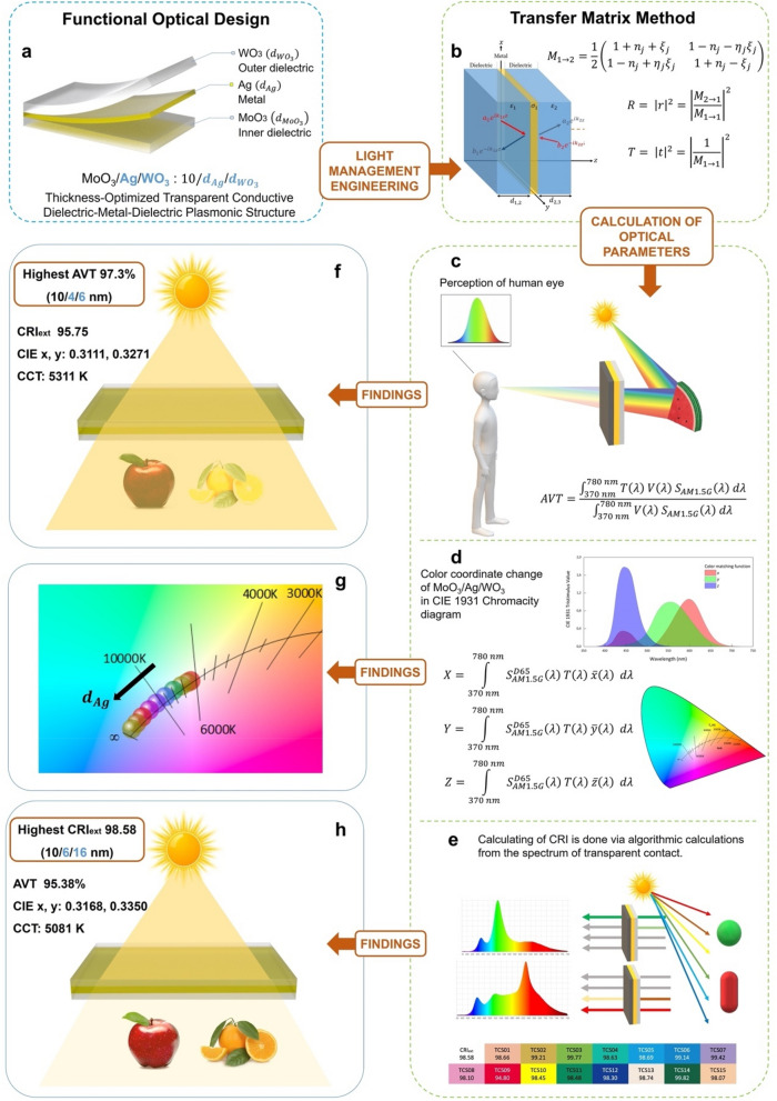
The present study sought to address the potential for use as a multi-purpose of MoO3/Ag/WO3 DMD transparent contact in various optoelectronic applications like semi-transparent solar cells, window applications, high-resolution LED technologies, lighting and, display technologies involving specific colour applications. By this means, we have functionally realized the contact design with optimal values of optical parameters such as AVT, CRI, CCT and colour coordinates by thickness optimizing of MoO3/Ag/WO3 in the mentioned application areas. We have employed the conventional Transfer Matrix Method (TMM) in calculations and made a detailed evaluation of the layer thickness dependent data. For the optimal MoO3/Ag/WO3 (10// nm) design, we have expressed the AVT, CRI and CCT from the findings of transfer matrix method. By its optical characteristic extracted, the current structure may be exhibited as a feasible transparent contact structure with a great colour rendering property. In this study, the methodology followed in the functional optical design of the transparent conductive plasmonic structure and the findings in its optical properties are given in Fig. 1.
Figure 1.
Functional optical design of transparent conductive plasmonic structure and its optical properties. (a) Schematic representation of MoO3/Ag/WoO3 transparent conductive plasmonic structure. (b) Transfer Matrix Method used in the calculation of optical characteristics and its application in Dielectric/Metal/Dielectric plasmonic structures. Calculation of optical parameters: (c) Evaluation of average visible transmittance calculated based on human eye perception. (d) Determination of CIE 1931 color coordinates. (e) Obtaining of color rendering index and test color samples. Findings in MoO3/Ag/WoO3 transparent conductive plasmonic structure, which is optimally designed by evaluating on the basis of optical parameters: (f) Highest Average Visible Transmittance. (g) Change of CIE 1931 color coordinates. (h) Highest color rendering index.
Result and discussion
It is evident that DMD based transparent contact structures have low resistance value (< 10 ), efficient charge injecting, and transmittance of more than 70%, particularly in the VR16,41. MoO3, which acts as an internal dielectric in the MoO3/Ag/WO3 transparent contact design, has relatively high hole mobility and high transparency in the VR10,42. That is why the potential of using MoO3 among TCOs with high work function in designing high-performance optoelectronic devices stands out. The use of MoO3, which provides a hole injection into active layers and acts as an anti-reflective layer for reflective metals such as Ag and Au, which have a high refractive index43,44, as HTL has become a well-established approach in inverted structures10,45–47. For optimal electrical performance, the thickness of MoO3 affected the electrical parameters of the devices is preferred around 10 nm28.
On the other hand, Ag is frequently preferred as a metal layer with a low absorption coefficient and high electrical conductivity than other common metals in DMD structures48,49. When an effective cap layer of WO3 is put to use due to its high refractive index and prevention of Ag oxidation50,51, the radiation loss from the surface plasmon in the Ag layer can be suppressed, and thus the thickness of WO3 () and the permeability of the DMD structure can be modified6,52.
By arguments of the sort mentioned above, a detailed evaluation of optical parameters such as AVT, extended CRI (CRIext), CCT, and colour coordinates of the MoO3/Ag/WO3 transparent contact designed within the scope of the study has been provided based on the thickness change of the metal and WO3 layers. For MoO3/Ag/WO3 (10// nm), the theoretical reflectance, transmittance and absorption spectra were calculated by ranging of 0–20 nm, the effective range where the actual physical changes can be observed. Subsequently, optical parameters of the structures were estimated from the spectra obtained by TMM.
Evaluation on AVT values of MoO3/Ag/WO3 structure
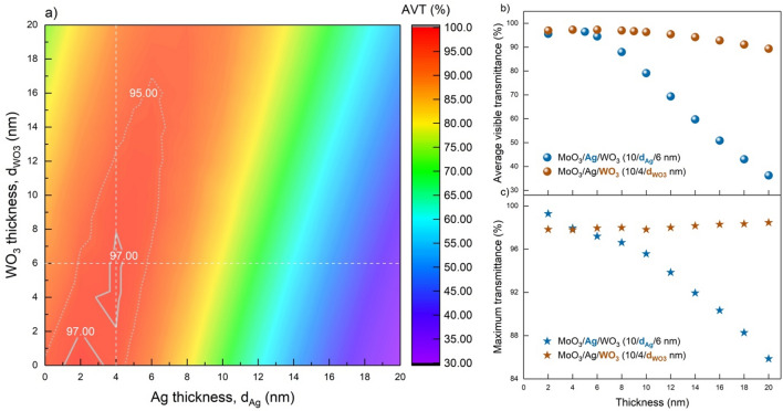
The first investigation for optimal MoO3/Ag/WO3 (10// nm) design was demonstrated depending on AVT. The and values dependence of the structure's associated AVT variation are exhibited in Fig. 2a. By varying and values in the range of 0–20 nm, the minimum AVT of the current structure was 32.48%, namely, it is widened to even higher levels than those of the lower limit (25%) for window applications. Based on our analysis, the MoO3/Ag/WO3 structure is a convenient transparent contact.
Figure 2.
Variation of AVT and transparency depending on the thickness of the transparent contact structure. (a) Mapping the AVT variation of the structure according to and values for MoO3/Ag/WO3 (10// nm). (b) AVT and, (c) values for structures of 10/4/ nm and 10//6 nm. Areas with solid grey lines and grey dashed lines have AVTs greater than 97% and 95%, respectively. The point where the white horizontal and vertical lines intersect gives the maximum AVT. It should be noted here that Ag is a determining layer for both AVT and maximum transparency, and outer dielectric WO3 acts as a waveguide. The encircling effect on the electromagnetic wave of WO3 causes an increment in maximum transparency with the increase of . Even the and values of 20 nm, AVT is greater than 25% which is the lower limit for window applications.
Increasing at a constant value of has little or no overall effect on AVT levels and the highest AVT was achieved for =4 nm and =6 nm. On the contrary, the increase in considerably affects on AVT. Particularly for greater than 8 nm of , the AVT tends to drop below 80%. Therefore, it is identified that Ag in the transparent contact structure exerts a more dominant role over the AVT. The present case can be explained by the reflection characteristic of Ag known in the VR, the electric field provided by the high free electron density, and the SP effect. As seen in AVT distributions, a significant linearity is observed between and (Fig. 2a). When this relationship between and is maintained in the MoO3/Ag/WO3 structure, the same AVTs can be obtained. In addition, for an electrical evaluation, in DMD structures in which Ag is a metal layer in the literature, with an increase of from 2 to 12 nm, resistivity and decrease from 5.97 × 10⁻⁵ cm to 0.97 × 10⁻⁵ cm and from 18.66 to 2.31 respectively53. Therefore, increasing significantly reduces AVT and increases conductivity.
In the AVT mapping of MoO3/Ag/WO3 (10// nm), the improvement in AVT with the increase of , especially for a specific larger than 6 nm, is due to the anti-reflection property of WO3 with the waveguide effect. Because it acts as the anti-reflection layer of WO3 for Ag with a high refraction index [1, 1:35, 1:36]. For a more effective evaluation of the anti-reflection feature, the change in the reflection spectra with the change of for 8 nm, 12 nm, 16 nm and 20 nm values of is given in Supplementary Fig. 4. In addition, a more effective anti-reflection feature with change by calculating the average reflection over AM1.5G for MoO3/Ag/WO3 (10// nm) is presented in Supplementary Fig. 5. ARAM1.5G is highly dependent on , but for a given Ag layer thicker than 6 nm, the reflection property of the structure is reduced by increasing .
CRIext, CIE x and y, CCT, maximum transmittance (Tmax) and wavelength () at Tmax, AVTs according to the MoO3/Ag/WO3 transparent contact structures change are presented in Table 1a. AVTs, estimated in this study, inside the areas with solid grey lines and grey dashed lines are greater than 97% and 95%, respectively (Fig. 2a). The lowest and highest AVTs of the DMD structure are 32.48% and 97.3% with =4 nm, =6 nm and with =20 nm, =2 nm respectively.
Table 1.
Optical parameters of the transparent contact structure at different thickness values.
| MoO3/Ag/WO3 (/) | AVT (%) | CRIext | CIE | CIE | CCT (K) | (%) | (nm) | |
|---|---|---|---|---|---|---|---|---|
| (a) | 4/6 | 97.3 | 95.75 | 0.3111 | 0.3271 | 5311 | 97.95 | 566.6 |
| 2/1 | 97 | 94.73 | 0.3118 | 0.3262 | 5273 | > 99 | 709 | |
| 2/20 | 84.58 | 96.67 | 0.3259 | 0.3359 | 4729 | > 99 | 968 | |
| 20/20 | 53.66 | 95.96 | 0.2483 | 0.2697 | 11,528 | 87.43 | 435 | |
| 20/2 | 32.48 | 95.82 | 0.2437 | 0.2488 | 14,821 | 79.68 | 384.2 | |
| (b) | 6/16 | 95.38 | 98.58 | 0.3168 | 0.3350 | 5081 | 97.09 | 582.2 |
| 14/12 | 68.26 | 98.23 | 0.2672 | 0.2882 | 8507 | 94.58 | 433 | |
| 14/6 | 59.74 | 97.16 | 0.2632 | 0.2793 | 9222 | 91.95 | 406.2 | |
| 4/6 | 97.3 | 95.75 | 0.3111 | 0.3271 | 5311 | 97.95 | 566.6 |
CRIext, CIE x and y, CCT, and values for MoO3/Ag/WO3 (10// nm) transparent contact structure for certain thicknesses according to various (a) AVT and (b) CRIext distributions. The / values given in bold are the optimal values with the highest AVT in the a section and, the highest CRIext in the b section.
When both Table 1a and Fig. 2a are interpreted, an increment in AVTs occurs with increasing , particularly for thicker than 10 nm. For example, in the MoO3/Ag/WO3 (10/20/20 nm), where the lowest AVT of 32.48% is observed, the AVT improves to 53.66% with the increase of to 20 nm. This is since the transparency reduced by the strong electric field and the plasmonic effect observed due to surface charges, especially in thicker metals, is improved with a thicker outer dielectric layer6,52. This effect is not dominant for the thin metal layer, and a reduction occurs with . In the high AVT region, while the AVT is 97% at =2 nm and =1 nm, the AVT decreases to 84.58% and contrarily increases to 20 nm.
In the case of =2 nm, is above 99% for =1 and 20 nm. Since the AVT has a maximum at 550 nm and is evaluated on AM1.5G, the deviation of from 550 nm reduces the AVTs even in the case of >99. Therefore, AVT is not at its maximum value in high-transparency structures, and values are considerably greater than 550 nm for these structures. With increasing from 2 to 20 nm, increases from 709 to 968 nm, and contrarily AVT decreases from 96.9% to 84.58%.
As seen in the AVT distribution of the MoO3/Ag/WO3 (10// nm), the intersection of the horizontal and vertical dashed lines corresponds to the values of =4 nm and =6 nm (Fig. 2a). The changes in AVT and along these horizontal and vertical lines for thicknesses varying in the range of 0–20 nm are introduced in Fig. 2b and c, respectively.
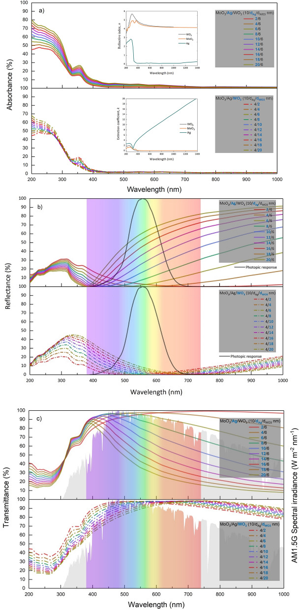
In a transparent contact structure, AVTs are more affected by the change of than . This optical characteristic can be understood when the absorption, reflectance and transmittance spectra of the MoO3/Ag/WO3 (Fig. 3a–c, respectively) are calculated by TMM according to the changes are examined. The AVTs are more sensitive to the change of than due to the significant increment in the reflection spectrum in the infrared region (IR) and VR. Because the absorption of the structure in this region is deficient and at wavelengths greater than 400 nm, the reflectance and transmittance characteristics are in exchange, as well as their sum is equal to 1. Therefore, increasing reflectance values by in VR decreases the transmittance values. Since AVT values are evaluated directly based on human eye perception, they decrease drastically compared to maximum transmittance.
Figure 3.
Optical spectra of the transparent contact structure. Variations of (a) absorption, (b) reflectance and (c) transmittance spectra dependent on and of MoO3/Ag/WO3 (10// nm) transparent contact structure. In a, wavelength dependent the refractive index () changes and extinction coefficient () of MoO3, WO3, and Ag are presented. It should be noted that the difference between the n values of MoO3 and WO3 drastically changes the distribution in the structure and allows for ultra-thin designs that allow easier modification of thickness control and optical characteristics. This enables the design of lighter and more flexible structures with the desired optical properties by using less material. The values in the VR for MoO3 and WO3 are very close to zero, allowing the evaluation of the direct trade-off between transmittance and reflectance without absorption. In b, the visible spectrum and the wavelength range from which the AVTs are calculated are given. In c, the photonic response of the human eye and the VR are presented as enveloped by AM1.5G. When the maximum value of the transparency coincides with the AM1.5G maximum, the highest AVT should be expected in the structure. In addition, the photonic response of human eye determines a wavelength range in the AVT calculations, and an evaluation should be made in this range.
When the absorption spectra given in Fig. 3a are examined, it is seen that the MoO3/Ag/WO3 transparent contact has very high absorption in the ultraviolet (UV) region. This is due to the known absorption characteristics of TMOs such as MoO3 and WO3 in the UV region. In the wavelength region more significant than 400 nm, MoO3 and WO3 have no absorption, and this characteristic indicates that the MoO3/Ag/WO3 system is a perfect transparent contact in VR.
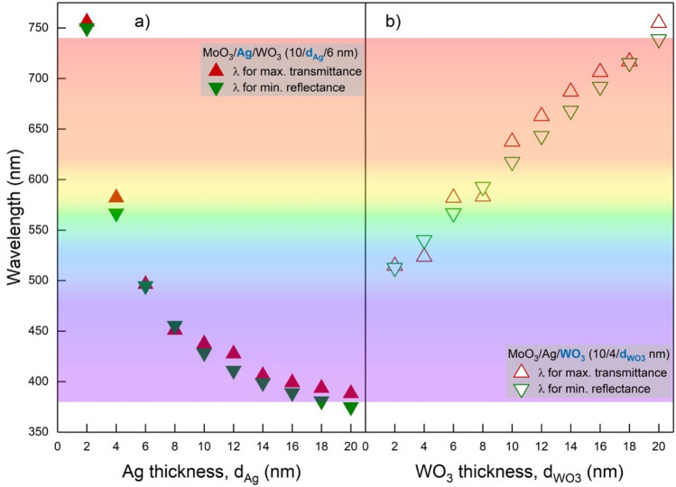
When the reflectance spectra given in Fig. 3b are examined, the wavelength value with the minimum reflection shifts to a lower wavelength with the increase of , while it shifts to higher wavelength values with the increase of . In addition, the increase in both and narrows the distribution of reflectance spectra. This behaviour observed in the reflection characteristic also manifests itself in the transmittance spectra, especially for the wavelength region with no absorption. The variation of wavelength values, at which minimum reflection and maximum transmittance are obtained, concerning and , are given in Fig. 4a and b, respectively.
Figure 4.
Maximum transmittance and reflectance values of the transparent contact structure. Wavelength changes of minimum reflectance and maximum transmittance corresponding to (a) and (b) values in MoO3/Ag/WO3 (10// nm) transparent contact structure. Particularly, structures with minimum reflection at wavelengths close to 550 nm can be used as antireflection in various optoelectronic devices. It can be designed that a transparent or an anti-reflection contact system is optimized for lower wavelengths with and for larger wavelengths with .
The minimum reflectance and maximum transmittance values for = 4 nm and = 6 nm are around 550 nm. Considering that AM1.5G and human eye perception have a maximum value at 550 nm, MoO3/Ag/WO3 system designed with = 4 nm and =6 nm has the potential to both transparent contact with high AVT for semi-transparent optoelectronic devices and an anti-reflection system for photovoltaic-based optoelectronic devices. In addition, due to the absorption characteristics of TMO’s in the UV region, there is a slight difference between the wavelengths belonging to the maximum transmittance and minimum reflectance for the same and .
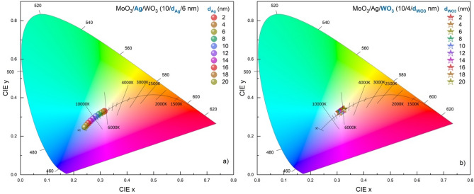
The effect of the metal layer on the transmittance and reflection spectra of the transparent contact, compared to the outer dielectric, which acts as a waveguide and has a surrounding effect, shows itself in the variation of the colour coordinates depending on the thickness. The variation of the colour coordinates of the MoO3/Ag/WO3 (10// nm) transparent contact structure concerning and are given in the CIE 1931 chromaticity diagram in Fig. 5a and b, respectively. The colour coordinates of the transparent contact with the highest AVT designed at = 4 nm and = 6 nm are CIE x = 0.3110 and CIE y = 0.3271. They are quite close to the colour coordinates of achromatic point (=0.3333, =0.3333), AM1.5G (=0.3202, =0.3324) and D65 (=0.3128, =0.3290). This superior performance, obtained in the colour characteristic of the MoO3/Ag/WO3 (10/4/6 nm) transparent contact structure with the highest AVT, increases the structure's potential to be used, especially in window applications that require neutral colour and in LED technologies.
Figure 5.
Colour coordinates of the transparent contact structure. In CIE 1931 Chromacity diagram, representation of colour coordinate changes corresponding to of MoO3/Ag/WO3 (10//6 nm) transparent contact structure. The black line in the diagrams shows the Planckian locus values for different CCTs. In the colour coordinates of the contact, a blue shift on the Planckian locus occurs with the variation.
With the increase of from 2 to 20 nm in the MoO3/Ag/WO3 (10//6 nm) transparent contact structure, The colour coordinates shifted from the achromatic point to the blue region along Planckian locus. CIE x decreased by 23.43% from 0.3154 to 0.2415, and CIE y decreased by 25.12% from 0.3299 to 0.2470. The blueshift is due to a serious decrease in the wavelengths responsible for the red colour and the IR region with the increase of , especially in the transmittance spectrum of the transparent contact structure. The effect of on colour coordinates is less than that of . This comparison can be better understood by examining the transmittance spectra given in Fig. 3b. With the increase of , the transmittance decreases, especially in the region where the colour matching functions are responsible for red, while the spectra of the transmittance spectra with change relatively at the same rate for all colours.
In determining the optimal conditions for the MoO3/Ag/WO3 transparent contact, the adjustment of should be made by evaluating the colour coordinates and AVTs together since the metal layer has a limiting effect on the AVT. However, even for =20 nm, the AVT of the transparent contact is 36.24%. This value is greater than 25%, considered the maximum limit for window applications. Therefore, this feature indicates that colour modification can be achieved with a metal layer in the MoO3/Ag/WO3 (10//6 nm) transparent contact structure. Especially for an LED that emits light in a different colour, integrating the MoO3/Ag/WO3 transparent contact into the structure with convenient design parameters can change the colour of the light emitted by the LED. In particular, the shift to blue offers significant potential for blue LED technology. In addition, the fact that the outer dielectric does not seriously affect the colour coordinates requires to be considered an effective parameter only in the evaluation of AVT.
Evaluation on CRI of MoO3/Ag/WO3 structure
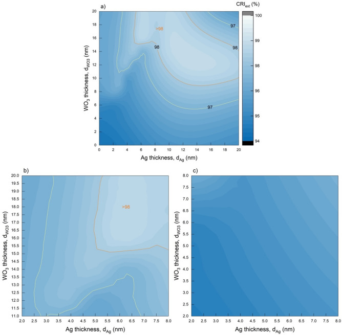
It is not sufficient for all optoelectronic devices to examine the characteristic of MoO3/Ag/WO3 transparent contact only in terms of AVT and colour coordinates and determine the optimal structure parameters. It is also essential to evaluate CRIs for optoelectronic devices such as LEDs, specially designed to serve lighting and high-resolution imaging technology. The ability of a light source to accurately reproduce the colours of an illuminated object is determined by the CRI, and values above 90 are classified as excellent. CRIs of 80 and above are acceptable for optoelectronic devices for indoor and commercial applications. However, it is crucial to obtain CRIs of 90 and above, especially for the exhibition and window lighting, screen display technologies where colour appearance is essential. The distribution of CRIext values for MoO3/Ag/WO3 (10// nm) calculated in the 0–20 nm range of and using the optical characteristics obtained by TMM is given in Fig. 6.
Figure 6.
CRIext mapping of transparent contact structure depending on thickness. Distribution of CRIext values corresponding to and for MoO3/Ag/WO3 (10// nm) in the range of (a) 0 < , < 20 nm, (b) 11 < < 20 nm and (c) 2 < < 8 nm. Areas with orange and yellow straight-line contours contain CRIext values greater than 98% and 97%, respectively.
AVT, CRIext, CIE x and y, CCT, Tmax and values of MoO3/Ag/WO3 transparent contact structure selected according to the variation of CRIext values and their maximum-minimum status are given in Table 1b. The CRIext values of the MoO3/Ag/WO3 (10// nm) transparent contact structure are above 94 for and in the range of 0–20 nm. This characteristic shows that the transparent contact structure has an excellent colour rendering property. Especially for >5 nm and >15 nm, CRIext takes values greater than 98. In the region of 7 > >5.5 nm and 20 > >15.5 nm, CRIext has a maximum value of 98.6. AVT, CRIext, CIE x and y, CCT, and values of MoO3/Ag/WO3 transparent contact structure selected according to the variation of CRIext values and their maximum-minimum status are given in Table 1b.
The CRIext of the MoO3/Ag/WO3 transparent contact structure, which is designed based on the highest AVT and neutral colour coordinates in the =4 nm and =6 nm parameters, is 95.75% and is not at its maximum value. Therefore, the optimal structure (=4 nm, =6 nm) determined based on AVT and neutral colour values may not show high performance when evaluated in terms of CRIext. Therefore, evaluating the AVT given in Fig. 2 and the CRIext distributions given in Fig. 6 together provides a more optimal structure.
When Fig. 3 and Table 1b are examined, it is evident that a thick outer dielectric layer is required to achieve high CRIext values. In this case, when the AVT distribution given in Fig. 2 is examined, should be in the range of 2–7 nm for high values. With a more detailed analysis, it is understood that = 6 nm and = 16 nm for both AVT and CRIext and neutral colour. For = 6 nm and = 16 nm, the AVT is 95.38%, the CRIext is maximum 98.58, and the CIE x and y colour coordinates are 0.3168 and 0.3350, respectively. In addition, in these structure parameters, is very close to 550 nm and has a value of 582.9 nm. Considering that commercial LEDs have reached 98 CRI today, with the achieved CRI of 98.58 and TCS09 of 94.80, MoO3/Ag/WO3 transparent contact for = 6 nm and = 16 has the potential to be highly applicable both as a transparent contact structure and conductive sheath for existing commercial LEDs and imaging technologies provided with them.
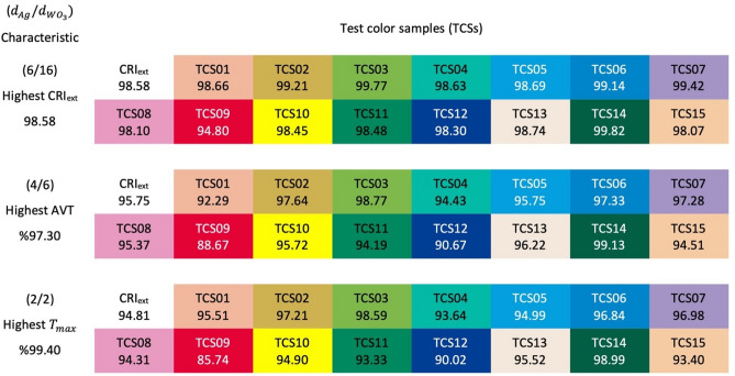
In addition to the CRIext evaluation, it is essential to know how the colour renderings of the optimally determined structures are for each test colour sample (TCS). TCS analysis determines which transparent contact structure to be used in various applications can give specific standard colour with which rendering and how faithfully it is. Within the scope of the study, colour renders analysis was performed by making calculations over 15 TCS for the MoO3/Ag/WO3 transparent contact structure. The TCS values for the MoO3/Ag/WO3 transparent contact structure with the highest AVT ( = 4 nm, = 6 nm), the highest CRIext = 6 nm, = 16 nm), and the highest transparency ( = 2 nm, = 2 nm) are given in Fig. 7.
Figure 7.
TCS classification of transparent contact structures. CRI for each test colour sample of MoO3/Ag/WO3 (10// nm) transparent contact structure with the highest AVT ( = 4 nm, = 6 nm), highest CRIext ( = 6 nm, = 16 nm) and highest transmittance ( = 2 nm, = 2 nm).
As expected for the structure with optimal values of = 6 nm and = 16 nm based on CRIext, there is a colour rendering index of over 90 for all TCSs. For structures designed based on AVT and Tmax, the values of all TCSs except TCS09 are pretty high and more significant than the perfection limit of 90. Therefore, the contact structure designed in these parameters is very suitable for optoelectronic applications such as lighting and display technologies that include specific colour applications. An electrical evaluation of MoO3/Ag/WO3 (10/6/16 nm), which is optimally presented for CRI, is also noteworthy in the literature. Especially, for > 4 nm, the decreases and becomes around 4 in = 6 nm53. Therefore, the MoO3/Ag/WO3 (10/6/16 nm) also has a very convenient contact properties for electrical performance.
TC09 measures how well a light source or transparent structure can reproduce red. The red colour is critical in applications such as photography, textiles and the production of human colour tones. Many objects around us appear as a mixture of colours, including red. For example, skin tone is very sensitive to the red colour of blood flowing under the skin. With all these features and its proximity to daylight or incandescent bulbs, the TCS09 stands out as a special consideration among other TCSs. A system with a low TCS09 score will display red as far from its colour, or even green. Therefore, the TCS09 is significant for LEDs, which form the backbone of daily or professional lighting technology today.
In analysis, it is not easy to obtain TCS09 at a high value compared to other TCSs, especially for mathematical evaluation over spectra. In addition, the TCS09 value is highly dependent on the spectral characteristics of the device. Therefore, the TCS09 rating is classified as suitable for values of 50 and above and excellent for values of 90 and above, unlike the CRI or CRIext scale. TCS09 values for MoO3/Ag/WO3 transparent contact designed based on AVT and are quite high and are 88.67 and 85.74, respectively. For the structure designed based on CRIext, the TCS09 metric is rated excellent and has a value of 94.80. Therefore, MoO3/Ag/WO3 (10// nm) transparent contact structure for = 6 nm and = 16 nm parameters is a high-performance contact system that can be integrated into optoelectronic devices based on LED lighting applications and imaging technologies.
When the are examined for the optimal structures presented in Fig. 7, it is remarkable that ultra-thin metal layer such as 2 nm, 4 nm and 6 nm is optimally presented. In practice, properties such as roughness and thickness of ultra-thin Ag films can significantly degrade the resistivity and sheet resistance. This is due to the formation process of the Ag layer, especially in physical vapor deposition techniques. Because it is usual for Ag particles to accumulate in islands during the deposition process. This requires the investigation of different transport mechanisms for the movement of electrons in the metal layer. Therefore, using various techniques such as sputtering and electron beam evaporation in the literature and improving the deposition parameters in these techniques, ultra-thin, ultra-smooth, continuous, low-loss and low- Ag thin films can be produced53,54. Especially in the sputter system, by increasing the sputtering time for Ag and narrowing the gap between Ag islands, for 4 nm Ag thin-film could be reduced considerably53. In addition, with the electron beam evaporation system, the root mean square roughness values could be improved from 0.73 nm to 0.22 nm even with the thinning of the thickness from 6 to 1 nm for ultra-thin Ag54. With all these developments and improvements in different deposition techniques for the production of ultra-fine Ags, the optimal structures presented in the study have the potential to be produced and offer good electrical properties.
Evaluation on colour Coordinates of MoO3/Ag/WO3 structure
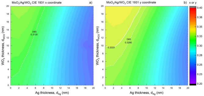
The colour perception and CRIext characteristics are also imperative to examine the colour coordinates of the MoO3/Ag/WO3 according to the and changes. The distribution of colour coordinates obtained from optical characteristics by TMM for MoO3/Ag/WO3 (10// nm) according to and was studied on. For and in the range of 0–20 nm is represented in Fig. 8.
Figure 8.
Mapping of the CIE 1931 colour coordinates of the transparent contact structure depending on the thickness. The distribution of (a) CIE x and, (b) y colour coordinates corresponding to the and values for MoO3/Ag/WO3 (10// nm). The dashed and solid white lines belong to the contours representing the colour coordinate of the D65 and achromatic point, respectively.
As mentioned in the AVT characteristic, examining the Fig. 8, it is seen that the metal layer is more effective than the outer dielectric on the colour coordinates. Also, the colour coordinates dependent on decrease after 7 nm for CIE x and 9 nm for CIE y. The obtainment colour coordinates very close to D65 and the achromatic point is possible for a wide range of and . On the other hand, the CIE x coordinate for the MoO3/Ag/WO3 (10// nm) contact cannot be at the Planckian locus value, but this is possible for the CIE y. A structure with colour characteristics of D65 coordinate can also be stated for MoO3/Ag/WO3 (10// nm), as seen from the D65 contour line in Fig. 8a and b. The optical parameters of the structures corresponding to the exact values of and are noted in Tables 2a and b. In addition, the change of colour coordinates and their relations with each other and together with and are given in Fig. 9a.
Table 2.
Optical parameters of transparent contact structure with colour over D65.
| (a) | (b) | ||||||||
|---|---|---|---|---|---|---|---|---|---|
| / | D65 | AVT(%) | CRIext | / | D65 | AVT(%) | CRIext | ||
| 8/19 | 0.3130 | 0.3341 | 94.19 | 98.18 | 10/20 | 0.3045 | 0.3290 | 91.21 | 98.44 |
| 6/14 | 0.3134 | 0.3324 | 95.89 | 97.01 | 9/18 | 0.3062 | 0.3292 | 92.78 | 98.44 |
| 5/11 | 0.3136 | 0.3309 | 96.5 | 96.37 | 8/16 | 0.3078 | 0.3293 | 94.12 | 98.03 |
| 4/8 | 0.3131 | 0.3291 | 96.97 | 95.76 | 7/14 | 0.3096 | 0.3297 | 95.22 | 97.42 |
| 3/6 | 0.3136 | 0.3289 | 97.016 | 95.32 | 6/12 | 0.3111 | 0.3297 | 96.07 | 96.82 |
| 5/10 | 0.3124 | 0.3297 | 96.66 | 96.27 | |||||
| 4/8 | 0.3131 | 0.3291 | 96.97 | 95.76 | |||||
| 2/5 | 0.3143 | 0.3290 | 96.22 | 95.04 | |||||
| 1/5 | 0.3153 | 0.3295 | 94.97 | 94.92 | |||||
Optical parameters of the structures corresponding to the exact values of and in the case that (a) CIE x and, (b) y coordinates are at D65.
Significant values are in [bold].
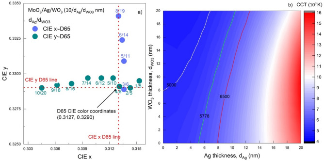
Figure 9.
Colour properties of the transparent contact structure with a CIE x and y on D65. (a) The colour coordinates' change of the structures corresponding to the exact values of and dependently the case that the CIE x and y colour coordinates of the MoO3/Ag/WO3 (10// nm) transparent contact are on the D65 point. (b) Mapping the CCT variation of the structure considering and values for MoO3/Ag/WO3 (10// nm). The white, green, and red-lined contours refer to the CCT values of 5000 K, 5778 K, and 6500 K, respectively.
As and decrease together in structures where the CIE x is equal to D65's x value, the CIE y coordinate also approaches its value in the D65 line. The same behaviour is obtained for structures where the coordinate is equal to D65. With this examination, as shown in Fig. 9a, the colour coordinate of the MoO3/Ag/WO3 transparent contact structure designed for nm and = 8 nm is equal to the D65 colour coordinates. In addition, the AVT and CRIext values for this structure are pretty high, with values of 96.97% and 95.76%, respectively.
The colour coordinates equal to D65 are the characteristic properties that make the current structure suitable for use in various optoelectronic applications, especially acting as a light source. Moreover, CCTs are noteworthy in optoelectronic devices designed for lighting technology, various light sources and illuminations closest to daylight. Here, CCTs were calculated from the optical characteristics of the MoO3/Ag/WO3 transparent contact structure obtained by TMM. The distribution of the values corresponding to and in the 0–20 nm range is given in Fig. 9b.
CCTs in the range of 5000–6500 K for MoO3/Ag/WO3 can be obtained for a wide value range of and . This characteristic shows that CCT is not limiting in optimising the MoO3/Ag/WO3 transparent contact. It can act as an illuminator quite close to daylight.
Method
Calculation of optic spectrum
The design of DMDs, which are transparent top contacts with MoO3/Ag/WO3 structure, was carried out by calculating the absorption, transmittance, reflection spectra and evaluating the thickness parameters. The transfer matrix method (TMM), a very effective one used in the simulations of optoelectronic devices, was applied to perform the calculations. It is the most potent and widely used method to analyze how the electromagnetic wave propagates in the structure and to determine the optical characteristics of the structure theoretically, especially in structures such as DMD, where different dielectric layers are grown on top of each other10. The method followed, and the equations used in calculating made with TMM are given in detail in our previous study10 and Supplementary Information.
Calculation of average visible transmittance
AVTs evaluate the transparency properties of contact systems and identify the transmittance characteristic in the visible light wavelength range (370–740 nm), taking into account the photonic response of the human eye. The transmittance spectra of the MoO3/Ag/WO3 system calculated by TMM were employed when making AVT calculations. The method followed, and the equations used in calculating AVTs are given in detail in our previous study10 and Supplementary Information.
Calculation of CIE 1931 colour coordinates
Another significant characteristic of transparent contact structures is the colour coordinates in the CIE 1931 chromaticity diagram (CIE x and y) as vital as AVT. Often used to determine the colour properties of transparent optoelectronic devices, the design of this diagram is based on the photonic response of the human eye. The method followed, and the equations used in calculating the CIE 1931 colour coordinates of the MoO3/Ag/WO3 transparent contact system are given in detail in our previous study10 and Supplementary Information.
Calculation of colour render ındex
Colour render index (CRI) measures how precise the colour of an object is when it is illuminated with an ideal or natural light source22. CRIs of 90 and above are considered excellent, while CRIs below 80 is generally considered poor40. Therefore, CRI creates a measurement system that gives whether the colours of illuminated objects are true to their originality and takes values in the range of 0–100. A CRI of 100 can be seen in standardised daylight sources or incandescent lamps. The method followed, and the equations used in calculating the CRIs of the MoO3/Ag/WO3 transparent contact system are given in detail in our previous study10 and Supplementary Information.
Calculation of correlated colour temperature
One key criterion of defining predominantly white light sources is that the associated colour temperature (CCT), a complete, one-dimensional measurement system, identifies a particular point along the blackbody curve on the CIE 1931 chromaticity diagram. CCT also emerges as a system that shows the similarity of optoelectronic devices with transparent or semi-transparent characteristics to light emitters in various technological applications. The method followed, and the equations used in calculating the CCTs of the MoO3/Ag/WO3 transparent contact system are given in detail in the Supplementary Information.
Supplementary Information
Author contributions
Ç.Ç. conceived the idea, conducted the study, performed the calculations and designed the Dielectric-Metal-Dielectric Plasmonic Structure, wrote the main manuscript text, E.Ç. performed the calculations, designed the Dielectric-Metal-Dielectric Plasmonic Structure, F.G. interpreted the optical spectra, did the critical revision and edited the main manuscript text, B.K. supervised the study.
Data availability
The datasets used and/or analysed during the current study available from the corresponding author on reasonable request.
Competing interests
The authors declare no competing interests.
Footnotes
Publisher's note
Springer Nature remains neutral with regard to jurisdictional claims in published maps and institutional affiliations.
Supplementary Information
The online version contains supplementary material available at 10.1038/s41598-022-13038-y.
References
- 1.Ji C, Liu D, Zhang C, Jay Guo L. Ultrathin-metal-film-based transparent electrodes with relative transmittance surpassing 100% Nat. Commun. 2020;11:3367. doi: 10.1038/s41467-020-17107-6. [DOI] [PMC free article] [PubMed] [Google Scholar]
- 2.Tom T, et al. Influence of co-sputtered Ag: Al ultra-thin layers in transparent V2O5/Ag:Al/AZO hole-selective electrodes for silicon solar cells. Materials. 2020;13:4905. doi: 10.3390/ma13214905. [DOI] [PMC free article] [PubMed] [Google Scholar]
- 3.Cattin L, Bernède JC, Morsli M. Toward indium-free optoelectronic devices: Dielectric/metal/dielectric alternative transparent conductive electrode in organic photovoltaic cells. Phys. Status Solidi a. 2013;210:1047–1061. doi: 10.1002/pssa.201228089. [DOI] [Google Scholar]
- 4.Giuliano G, et al. Nonprecious copper-based transparent top electrode via seed layer-assisted thermal evaporation for high-performance semitransparent n-i-p perovskite solar cells. Adv. Mater. Technol. 2019;4:1800688. doi: 10.1002/admt.201800688. [DOI] [Google Scholar]
- 5.Maniyara RA, Mkhitaryan VK, Chen TL, Ghosh DS, Pruneri V. An antireflection transparent conductor with ultralow optical loss (<2 %) and electrical resistance (<6 Ω sq−1) Nat. Commun. 2016;7:13771. doi: 10.1038/ncomms13771. [DOI] [PMC free article] [PubMed] [Google Scholar]
- 6.Yeh T-H, et al. Vacuum-deposited MoO3/Ag/WO3 multilayered electrode for highly efficient transparent and inverted organic light-emitting diodes. Org. Electron. 2018;59:266–271. doi: 10.1016/j.orgel.2018.05.014. [DOI] [Google Scholar]
- 7.Bae S, et al. Roll-to-roll production of 30-inch graphene films for transparent electrodes. Nat. Nanotechnol. 2010;5:574–578. doi: 10.1038/nnano.2010.132. [DOI] [PubMed] [Google Scholar]
- 8.Lipomi DJ, et al. Skin-like pressure and strain sensors based on transparent elastic films of carbon nanotubes. Nat. Nanotechnol. 2011;6:788–792. doi: 10.1038/nnano.2011.184. [DOI] [PubMed] [Google Scholar]
- 9.Wan J, et al. Tunable broadband nanocarbon transparent conductor by electrochemical intercalation. ACS Nano. 2017;11:788–796. doi: 10.1021/acsnano.6b07191. [DOI] [PubMed] [Google Scholar]
- 10.Çetinkaya Ç, et al. Design and fabrication of a semi-transparent solar cell considering the effect of the layer thickness of MoO3/Ag/MoO3 transparent top contact on optical and electrical properties. Sci. Rep. 2021;11:1–17. doi: 10.1038/s41598-021-92539-8. [DOI] [PMC free article] [PubMed] [Google Scholar]
- 11.Hecht DS, Hu L, Irvin G. Emerging transparent electrodes based on thin films of carbon nanotubes, graphene, and metallic nanostructures. Adv. Mater. 2011;23:1482–1513. doi: 10.1002/adma.201003188. [DOI] [PubMed] [Google Scholar]
- 12.Dou L, et al. Solution-processed copper/reduced-graphene-oxide core/shell nanowire transparent conductors. ACS Nano. 2016;10:2600–2606. doi: 10.1021/acsnano.5b07651. [DOI] [PubMed] [Google Scholar]
- 13.Maurer JHM, González-García L, Reiser B, Kanelidis I, Kraus T. Templated self-assembly of ultrathin gold nanowires by nanoimprinting for transparent flexible electronics. Nano Lett. 2016;16:2921–2925. doi: 10.1021/acs.nanolett.5b04319. [DOI] [PubMed] [Google Scholar]
- 14.Zhang Y, et al. Broadband transparent electrode in visible/near-infrared regions. ACS Photon. 2021;8:2203–2210. doi: 10.1021/acsphotonics.1c00515. [DOI] [Google Scholar]
- 15.Kwon JH, et al. Functional design of dielectric–metal–dielectric-based thin-film encapsulation with heat transfer and flexibility for flexible displays. ACS Appl. Mater. Interfaces. 2017;9:27062–27072. doi: 10.1021/acsami.7b06076. [DOI] [PubMed] [Google Scholar]
- 16.Guillén C, Herrero J. TCO/metal/TCO structures for energy and flexible electronics. Thin Solid Films. 2011;520:1–17. doi: 10.1016/j.tsf.2011.06.091. [DOI] [Google Scholar]
- 17.Gray SK. Theory and modeling of plasmonic structures. J. Phys. Chem. C. 2013;117:1983–1994. doi: 10.1021/jp309664c. [DOI] [Google Scholar]
- 18.Singh HK, Arunachalam B, Kumbhar S, Sharma P, Solanki CS. Opto-electrical performance improvement of mono c-Si solar cells using dielectric–metal–dielectric (D-M-D) sandwiched structure-based plasmonic anti-reflector. Plasmonics. 2016;11:323–336. doi: 10.1007/s11468-015-0049-5. [DOI] [Google Scholar]
- 19.Wu M, Yu S, He L, Yang L, Zhang W. High quality transparent conductive Ag-based barium stannate multilayer flexible thin films. Sci. Rep. 2017;7:103. doi: 10.1038/s41598-017-00178-9. [DOI] [PMC free article] [PubMed] [Google Scholar]
- 20.Choi DK, et al. Highly efficient, heat dissipating, stretchable organic light-emitting diodes based on a MoO3/Au/MoO3 electrode with encapsulation. Nat. Commun. 2021;12:2864. doi: 10.1038/s41467-021-23203-y. [DOI] [PMC free article] [PubMed] [Google Scholar]
- 21.Ren X, Li X, Choy WCH. Optically enhanced semi-transparent organic solar cells through hybrid metal/nanoparticle/dielectric nanostructure. Nano Energy. 2015;17:187–195. doi: 10.1016/j.nanoen.2015.08.014. [DOI] [Google Scholar]
- 22.Upama MB, et al. High-efficiency semitransparent organic solar cells with non-fullerene acceptor for window application. ACS Photon. 2017;4:2327–2334. doi: 10.1021/acsphotonics.7b00618. [DOI] [Google Scholar]
- 23.Betancur R, et al. Transparent polymer solar cells employing a layered light-trapping architecture. Nat. Photon. 2013;7:995–1000. doi: 10.1038/nphoton.2013.276. [DOI] [Google Scholar]
- 24.Yu W, et al. Highly efficient semitransparent polymer solar cells with color rendering index approaching 100 using one-dimensional photonic crystal. ACS Appl. Mater. Interfaces. 2015;7:9920–9928. doi: 10.1021/acsami.5b02039. [DOI] [PubMed] [Google Scholar]
- 25.Lipomi DJ, Tee BC, Vosgueritchian M, Bao Z. Stretchable organic solar cells. Adv. Mater. 2011;23:1771–1775. doi: 10.1002/adma.201004426. [DOI] [PubMed] [Google Scholar]
- 26.Yang T, et al. Inverted polymer solar cells with 8.4% efficiency by conjugated polyelectrolyte. Energy Environ. Sci. 2012;5:8208. doi: 10.1039/c2ee22296e. [DOI] [Google Scholar]
- 27.Li Z, Ma T, Yang H, Lu L, Wang R. Transparent and colored solar photovoltaics for building integration. Solar RRL. 2021;5:1–21. [Google Scholar]
- 28.Çetinkaya Ç, et al. Evaluation on output parameters of the inverted organic solar cells depending on transition-metal-oxide based hole-transporting materials. Opt. Mater. (Amst) 2021;120:111457. doi: 10.1016/j.optmat.2021.111457. [DOI] [Google Scholar]
- 29.Najafi-Ashtiani H, Akhavan B, Jing F, Bilek MM. Transparent conductive dielectric−metal−dielectric structures for electrochromic applications fabricated by high-power impulse magnetron sputtering. ACS Appl. Mater. Interfaces. 2019;11:14871–14881. doi: 10.1021/acsami.9b00191. [DOI] [PubMed] [Google Scholar]
- 30.Dong W, et al. Bifunctional MoO3–WO3/Ag/MoO3–WO3 films for efficient ITO–free electrochromic devices. ACS Appl. Mater. Interfaces. 2016;8:33842–33847. doi: 10.1021/acsami.6b12346. [DOI] [PubMed] [Google Scholar]
- 31.Thakur VK, Ding G, Ma J, Lee PS, Lu X. Hybrid materials and polymer electrolytes for electrochromic device applications. Adv. Mater. 2012;24:4071–4096. doi: 10.1002/adma.201200213. [DOI] [PubMed] [Google Scholar]
- 32.Yan C, et al. Stretchable and wearable electrochromic devices. ACS Nano. 2014;8:316–322. doi: 10.1021/nn404061g. [DOI] [PubMed] [Google Scholar]
- 33.Yin Y, Lan C, Guo H, Li C. Reactive sputter deposition of WO3/Ag/WO3 film for indium tin oxide (ITO)-free electrochromic devices. ACS Appl. Mater. Interfaces. 2016;8:3861–3867. doi: 10.1021/acsami.5b10665. [DOI] [PubMed] [Google Scholar]
- 34.Li H, Lv Y, Zhang X, Wang X, Liu X. High-performance ITO-free electrochromic films based on bi-functional stacked WO3/Ag/WO3 structures. Sol. Energy Mater. Sol. Cells. 2015;136:86–91. doi: 10.1016/j.solmat.2015.01.002. [DOI] [Google Scholar]
- 35.Wen R-T, Malmgren S, Granqvist CG, Niklasson GA. Degradation dynamics for electrochromic WO3 films under extended charge insertion and extraction: unveiling physicochemical mechanisms. ACS Appl. Mater. Interfaces. 2017;9:12872–12877. doi: 10.1021/acsami.7b01324. [DOI] [PubMed] [Google Scholar]
- 36.Cattin L, Louarn G, Morsli M, Bernède JC. Semi-transparent organic photovoltaic cells with dielectric/metal/dielectric top electrode: influence of the metal on their performances. Nanomaterials. 2021;11:393. doi: 10.3390/nano11020393. [DOI] [PMC free article] [PubMed] [Google Scholar]
- 37.Gong Y, et al. Diverse applications of MoO3 for high performance organic photovoltaics: fundamentals, processes and optimization strategies. J. Mater. Chem. A. 2020;8:978–1009. doi: 10.1039/C9TA12005J. [DOI] [Google Scholar]
- 38.Cattin L, et al. MoO3 surface passivation of the transparent anode in organic solar cells using ultrathin films. J. Appl. Phys. 2009;105:034507. doi: 10.1063/1.3077160. [DOI] [Google Scholar]
- 39.Ohta N, Robertson AR. Colorimetry: Fundamentals and applications. New York: Wiley; 2005. [Google Scholar]
- 40.Zhang H, et al. Transparent organic photodetector using a near-infrared absorbing cyanine dye. Sci. Rep. 2015;5:9439. doi: 10.1038/srep09439. [DOI] [PMC free article] [PubMed] [Google Scholar]
- 41.Kim S, Lee J-L. Design of dielectric/metal/dielectric transparent electrodes for flexible electronics. J. Photon. Energy. 2012;2:021215. doi: 10.1117/1.JPE.2.021215. [DOI] [Google Scholar]
- 42.Qin P, et al. Transition metal oxides as hole-transporting materials in organic semiconductor and hybrid perovskite based solar cells. Sci. China Chem. 2017;60:472–489. doi: 10.1007/s11426-016-9023-5. [DOI] [Google Scholar]
- 43.Tubbs MR. MoO3 layers — optical properties, colour centres, and holographic recording. Physica Status Solidi (a) 1974;21:253–260. doi: 10.1002/pssa.2210210127. [DOI] [Google Scholar]
- 44.Anwar M, Hogarth CA. Optical properties of amorphous thin films of MoO3 deposited by vacuum evaporation. Physica Status Solidi (a) 1988;109:469–478. doi: 10.1002/pssa.2211090213. [DOI] [Google Scholar]
- 45.Kyaw AKK, et al. An inverted organic solar cell employing a sol-gel derived ZnO electron selective layer and thermal evaporated MoO3 hole selective layer. Appl. Phys. Lett. 2008;93:221107. doi: 10.1063/1.3039076. [DOI] [Google Scholar]
- 46.Tao C, et al. Performance improvement of inverted polymer solar cells with different top electrodes by introducing a MoO3 buffer layer. Appl. Phys. Lett. 2008;93:2006–2009. [Google Scholar]
- 47.Ullah I, et al. Enhanced efficiency of organic solar cells by using ZnO as an electron-transport layer. Mater. Res. Exp. 2017;4:125505. doi: 10.1088/2053-1591/aa9dc9. [DOI] [Google Scholar]
- 48.Schulz LG. The optical constants of silver, gold, copper, and aluminum i the absorption coefficient k. J. Opt. Soc. Am. 1954;44:357. doi: 10.1364/JOSA.44.000357. [DOI] [Google Scholar]
- 49.Schulz LG, Tangherlini FR. Optical constants of silver, gold, copper, and aluminum ii the index of refraction n. J. Opt. Soc. Am. 1954;44:362. doi: 10.1364/JOSA.44.000362. [DOI] [Google Scholar]
- 50.Hutchins MG, Abu-Alkhair O, El-Nahass MM, El-Hady KA. Structural and optical characterisation of thermally evaporated tungsten trioxide (WO3) thin films. Mater. Chem. Phys. 2006;98:401–405. doi: 10.1016/j.matchemphys.2005.09.052. [DOI] [Google Scholar]
- 51.Patel KJ, Panchal CJ, Kheraj VA, Desai MS. Growth, structural, electrical and optical properties of the thermally evaporated tungsten trioxide (WO3) thin films. Mater. Chem. Phys. 2009;114:475–478. doi: 10.1016/j.matchemphys.2008.09.071. [DOI] [Google Scholar]
- 52.Gramotnev DK, Bozhevolnyi SI. Plasmonics beyond the diffraction limit. Nat. Photonics. 2010;4:83–91. doi: 10.1038/nphoton.2009.282. [DOI] [Google Scholar]
- 53.Zhang D, et al. Effect of silver evolution on conductivity and transmittance of ZnO/Ag thin films. J. Appl. Phys. 2011;109:104318. doi: 10.1063/1.3592975. [DOI] [Google Scholar]
- 54.Chen W, Thoreson MD, Ishii S, Kildishev AV, Shalaev VM. Ultra-thin ultra-smooth and low-loss silver films on a germanium wetting layer. Opt. Exp. 2010;18:5124. doi: 10.1364/OE.18.005124. [DOI] [PubMed] [Google Scholar]
Associated Data
This section collects any data citations, data availability statements, or supplementary materials included in this article.
Supplementary Materials
Data Availability Statement
The datasets used and/or analysed during the current study available from the corresponding author on reasonable request.


