

Abstract

The modeling of functional photonic devices that rely on molecular materials continues to be a major contemporary challenge. It is a challenge because, in the Maxwell equations, which govern the light-matter interaction, material properties are primarily introduced on phenomenological grounds and not from first principles. To overcome such limitations, we outline a multiscale modeling approach that bridges multiple length scales. We can predict with our approach the optical response of a photonic device that exploits in its design molecular materials whose properties were determined using time-dependent density functional theory. The specifically considered device is a broadband perfect absorber that uses in part a thin film comprising gold molecules made from 144 atoms. Our methodology discloses various chemical and physical effects that define such a device’s response. Our methodology is versatile, and a larger number of applications will profit from this development.
Introduction
Nanotechnology links atomic constituents to macroscopic applications and devices. While nanotechnological systems require a quantum mechanical description to capture their properties, classical and continuum descriptions are required when considering the devices at the macroscopic scale. The development of a scale-bridging computational methodology to predict the properties of such systems is a prime scientific challenge. The developments are worth spending and motivated by many promising devices applicable to selected needs.
Generally, scale-bridging computational methods have been developed in multiple application areas. One approach is simultaneously solving quantum mechanics (QM) and electromagnetic (EM) equations to study electronic devices, known as the QM/EM method.1 The quantum part explains the device’s electronic structure, and the classical electrodynamic part describes the electrodynamic interaction between the device and its background. Molecular dynamics (MD) has been used to understand the mechanics of molecules at the atomic scale.2 Using the outcomes from MD simulations, multiscale physics problems in objects such as nanopores can be bridged to an object on a larger scale,3,4 or when studying nucleation processes of metals and colloids.5 The finite-element method can also be used to study microstructures like grains6 or analyze the linear elastodynamics properties of objects across different scales.7
In the current work, we are interested in optical devices based on metallic nanoparticles as the molecular building blocks. Nanoparticles constitute a versatile platform where sizes, shapes, and materials can be deterministically tailored to create and enhance selected applications. For example, controlling protein orientations8 and measuring gravity has been implemented using quantum levitated nanoparticles.9 Sensing a few kinds of small bio-objects is now possible thanks to the strong and narrow optical resonances of the nanoparticles at desired frequencies.10−13 A metal nanoparticle coupled to a quantum emitter can emit single photons at a high repetition rate.14
The system we are interested in utilizes metal nanoparticles as a core in a thin film device that perfectly absorbs light in an extended spectral region. Experimentally, synthesizing the nanoparticles is possible through self-assembly of the nanoparticles,15 which has been reported for perfect absorber application.16 These perfect broadband absorbers shall have an operating frequency between the near-infrared and the UV region.17−19 The requirement for their functionality is simple: Absorb as much as possible light in a predefined spectral range. While many variations can be considered, a generic perfect absorber consists of three layers. At the bottom, there is a sufficiently thick metallic film that serves as a ground plate. It reflects the light and prevents transmission through the thin film stack. The top layer contains lossy metallic nanoparticles. Here, the light shall be predominantly absorbed where it can be harvested for selected applications. Finally, the central layer, frequently called the spacer layer, is a dielectric layer with a carefully chosen thickness.20 The dispersive response of the system allows achieving this effect spectrally broadband.21 But of course, this requires dedicated adjustments of all degrees of freedom, such as size, shape, and material of individual nanoparticles, the density of the nanoparticles in the top layer, and the material and the thickness of the spacer layers, not to mention the polarization and the angle of incidence of the incoming light.
For a deterministic design, we need to implement a methodology that reliably predicts the macroscopic response of such systems from an accurate description of its constituents. As the nanoparticles can be extremely tiny, when fabricated as clusters,22−24 such description shall start from a quantum-chemical description of the metallic molecules. Then, the outcome from such analysis is fueled into an optical simulation of the device that allows its optimization. Such scale-bridging simulation has not yet been reported and is developed in this work.
The perfect absorber contains metallic nanoparticles in the form of what we call metallic molecules. The considered metallic molecules consist of 144 gold atoms (Au144).25,26 However, this should merely be taken as an example. Au144 is a stable gold structure, and it corresponds to the bulk gold nanoparticles that would have been considered in a pure classical simulation.
The quantum mechanical description can be based on time-dependent density functional theory (TDDFT), density functional tight binding, empirical tight-binding, or fragment molecular-orbital. In our case, TDDFT is already proven to be able to analyze the plasmon response from resonant excitation of a superposition of single-electron transitions of a molecule.27 Afterward, we use the notion of a T-matrix28 to bridge the calculation from the quantum mechanical-based simulation to the classical Maxwell equation-based simulations if we start to look at a cluster of metal molecules in a thin film. The T-matrix is a matrix that expresses the electromagnetic response of a scatterer and/or a system of scatterers in a suitable algebraic language.
With the purpose to bridge multiple length scales, we first consider a larger number of metallic molecules and let them form a cluster, i.e., an assembly of metallic nanoparticles. The cluster is sufficiently large to capture the statistical details of the nanoparticle arrangement while sufficiently small so that we can still apply a full-wave solution of Maxwell’s equations to capture its response. The optical properties of such a cluster are expressed in terms of a global T-matrix.
Afterward, we compute the optical response from a periodic and dense arrangement of such a cluster of nanoparticles. We do so by solving the self-consistent scattering problem where the renormalization of the T-matrix, thanks to the interaction with all clusters forming the film, is considered. To bridge a further length scale and neglect the very fine details of the layer containing the metallic molecules, we invert the reflection and transmission coefficients from the thin film using a methodology from the field of metamaterials to assign an effective permittivity to it.
Using this effective property, we can use a thin film transfer matrix technique to study the optical response from the considered layer stacks. While suitably adjusting the individual layer thicknesses, we can maximize the objective function. Following the motivation, we consider exemplarily the absorption of light in an extended spectral region as the objective function.
With this approach, we describe a flexible and versatile methodology for the multiscale modeling of optical devices made from constituents that require a quantum mechanical treatment. Objects with smaller length scales, like molecules, are studied in detail, and only their primary optical response is considered to represent these objects at the following larger length scale. We stress that material properties are not introduced here on phenomenological grounds. In contrast, we consider materials explicitly using quantum mechanical methods. As a result, our work can be applied to a multitude of further considerations. Despite this, some approximations need to be done to describe the system as reliable and to predict macroscopic properties.
The article is structured into an extended Methods section, where we describe the considered methods used in our workflow, and a Results and Discussion section, where we present and discuss the actual results when considering a specific structure.
Methods
Quantum Simulations
Polarizabilities from Linear Response DFT
The frequency-dependent
electronic polarizability tensor  needed to construct the T-matrix for the
individual metallic molecule is obtained from a first-principles approach.
Using linear-response time-dependent density functional theory (LR-TDDFT),
the frequency-dependent response equation can be formulated as a coupled-perturbed
Kohn–Sham (CPKS) for each Cartesian component γ as equation29−31
needed to construct the T-matrix for the
individual metallic molecule is obtained from a first-principles approach.
Using linear-response time-dependent density functional theory (LR-TDDFT),
the frequency-dependent response equation can be formulated as a coupled-perturbed
Kohn–Sham (CPKS) for each Cartesian component γ as equation29−31
| 1 |
with the 2 × 2 supermatrices
| 2 |
Xγ and Yγ in eq 1 are the solution vectors needed to obtain the desired polarizability. Furthermore, Pγ and Qγ collect the integrals describing the external perturbation. In the case of (frequency-dependent) dipole polarizabilities, these are the electric dipole integrals given by
| 3 |
| 4 |
where ϕκ are the orbital basis functions and Cκp and Cλ are the atomic-orbital to molecular-orbital transformation coefficients obtained from solving the Kohn–Sham equations for the ground state. Note that the integrals ⟨ϕκ | μγ | ϕλ⟩ are equivalent with those used to calculate the ground state electric dipole moment for the three Cartesian components γ ∈ {x, y, z}. Within the adiabatic approximation and further assuming that the wavelength of the perturbation is significantly longer than the size of the nanostructures investigated in this work, the coupling matrices in eq 2 are given as
| 5 |
| 6 |
ϵi and ϵa in eq 5 refer to the occupied and virtual Kohn–Sham orbital energies respectively, via, jb is a standard Coulomb integral describing electron repulsion
| 7 |
and fia, jbXC is the second derivative of the exchange-correlation (XC) energy
| 8 |
where EXC is the exchange-correlation energy expression within the chosen density functional approximation. via, bjCOSMO is the potential energy contribution of the implicit conductor-like screening model (COSMO) used to incorporate effects of the chemical surrounding.32,33 The COSMO term is convenient, as it is far more efficient to describe the surrounding by a polarizable medium, modeled by its dielectric function and the refractive index, instead of adding further atomistic regions to the ab initio DFT region. For a detailed discussion of COSMO, we refer the reader to ref (32). Finally, the frequency-dependent dipole polarizability αe(ω) tensor is obtained from the solution vectors {Xγ(ω), Yγ(ω)} of eq 1 for each Cartesian component γ, and the integrals {Pγ′, Qγ′} for each Cartesian component γ′ by means of the direct product
| 9 |
To obtain the polarizability tensor  of a
molecule at a given complex frequency
ω, where the real part marks the absorption/emission frequency
and the imaginary part determines the line broadening, one CPKS equation
at eq 1 needs to be solved
for each Cartesian direction. In total, for N frequencies
of interest, 3N CPKS equations need to be solved.
The outcome from the analysis is the polarizability tensor
of a
molecule at a given complex frequency
ω, where the real part marks the absorption/emission frequency
and the imaginary part determines the line broadening, one CPKS equation
at eq 1 needs to be solved
for each Cartesian direction. In total, for N frequencies
of interest, 3N CPKS equations need to be solved.
The outcome from the analysis is the polarizability tensor  that expresses how the
molecular object,
i.e., an individual metallic molecule, responds to an external electromagnetic
field. We have considered here only the electric dipole approximation.
Such electric dipole approximation is, nevertheless, entirely sufficient
for the particles at stake. Also, while outlined for TD-DFT in this
work, recent developments have shown that also the GW–Bethe–Salpeter equation method can be applied to solve eq 1.31,34
that expresses how the
molecular object,
i.e., an individual metallic molecule, responds to an external electromagnetic
field. We have considered here only the electric dipole approximation.
Such electric dipole approximation is, nevertheless, entirely sufficient
for the particles at stake. Also, while outlined for TD-DFT in this
work, recent developments have shown that also the GW–Bethe–Salpeter equation method can be applied to solve eq 1.31,34
As outlined in the following subsections, it is straightforward to convert the obtained electric dipole polarizabilities to T-matrices, which can be injected into an appropriate framework to simulate properties of larger ensembles of molecules, which are difficult to tackle using DFT alone due to their size.
Classical Simulations
Using the polarizability of the object calculated on quantum mechanical grounds, we can study the optical response of the more macroscopic system on classical grounds. A sequence of tools is applied to climb up the ladder of length scales. First, we start from the classical description of the individual metallic molecule. Next, we go to a cluster of such metallic molecules and afterward to a thin film of such clusters to which we assign effective properties. Finally, using such a homogeneous description, we study and optimize the optical response of the perfect absorber by considering reflectance, transmittance, and absorptance of a suitably chosen layer stack.
Description of an Individual Metallic Molecule
At first, we consider an isolated metallic molecule, i.e., the individual nanoparticle, to be placed in homogeneous and isotropic media and illuminated by a time-harmonic plane wave. We describe its optical action classically using a T-matrix that we obtain from the quantum-chemical simulations described above. For that, all we need to do is to convert the electric dipolar polarizability to the T-matrix. Keeping in mind that our scattering problem is formulated in spherical coordinates while the polarizability has been calculated in a Cartesian, this is merely a basis change written as28
 |
10 |
where  is the
electric polarizability tensor in
dipole approximation obtained from the quantum-chemical simulation, c is the speed of light in the background medium, Z is the impedance of the background medium, and
is the
electric polarizability tensor in
dipole approximation obtained from the quantum-chemical simulation, c is the speed of light in the background medium, Z is the impedance of the background medium, and  is the inverse of the
3 × 3 unitary
change of basis matrix that goes from the Cartesian to the spherical
basis, for the dipole term.
is the inverse of the
3 × 3 unitary
change of basis matrix that goes from the Cartesian to the spherical
basis, for the dipole term.
When describing the light scattering from a spatially confined object in the T-matrix approach, we expand the incident and scattered electric field at a specific frequency ω using vector spherical harmonics (VSH)
| 11 |
| 12 |
where Nnm(ω, r) are the electric VSHs and Mnm(ω, r) are the magnetic VSHs. The VSHs are chosen to ensure boundary conditions for the different fields, expressed in the respective superscript (1) and (3). The VSH expand the fields relative to the center of the considered nanoparticle.
The expansion comes with their respective expansion coefficients {anm, bnm} for the incident field and {pnm, qnm} for the scattered field. The index n characterizes the multipolar order of the expansion. n = 1 corresponds to the dipole term, n = 2 to the quadrupolar term etc. The sum of the field from all the multipolar terms results in the full incident or scattered field. When considering an isolated metallic molecule, we truncate the expansion to the electric dipole term. However, higher-order multipole moments are also considered when considering a larger number of metallic molecules to form a cluster.
Now, the T-matrix relates the incident field to the scattered field by a matrix equation
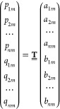 |
13 |
It implies that a matrix multiplication can compute the scattered field for a given incident field and a known object, characterized by its T-matrix. From that, observable properties can be calculated. Ensemble-averaged values that consider a possible random orientation of the nanoparticles relative to the incident field are defined on the base of a trace over the T-matrix. For example, the extinction cross section is defined as35
| 14 |
and the scattering cross section can be defined as
| 15 |
where  is the wavenumber in the background
medium.
The absorption cross section is then the difference between extinction
and scattering cross section
is the wavenumber in the background
medium.
The absorption cross section is then the difference between extinction
and scattering cross section
| 16 |
Description of a Cluster of Metallic Molecules
At this stage, we can classically describe the interaction of light with an individual metallic molecule placed in SiO2 as the background medium. This was considered throughout this work as the host medium in both the quantum-chemical and the classical Maxwell simulations.
However, Au144 has a diameter of roughly 1.5 nm, which is still extremely tiny. Nevertheless, at this length scale, the interaction to the nearest neighbor matters, and we wish to quantify that interaction precisely while being on the grounds of Maxwell’s equations. We stress that we can no longer describe charge transfer effects among adjacent metallic molecules. However, that is also safely supposed to be negligible since neighboring metallic molecules have a greater distance than the atomic spacing. Therefore, we consider a larger number of clustered metallic molecules and describe their interaction with light at the level of a Maxwell full-wave solver. The purpose is to assign to that cluster a T-matrix that describes the interaction of light with the cluster. In contrast to the discussion in the previous sub-subsection, this global T-matrix captures the optical action from many metallic molecules. Therefore, while a description in the electric dipole approximation was sufficient for the individual metallic molecule, we consider now an electric dipolar and a magnetic dipolar contribution to the scattering response. Higher-order terms could have been considered as well but are, indeed, negligible for our metallic cluster.
In anticipation of the description at the next higher level of aggregation, we pack the Au144 gold molecules into a cubical unit cell. At this level, the metallic molecules are approximated as individual spherical nanoparticles (please see Figure 1a). We will consider the Au144 molecular structure as a sphere. More detailed information about the Au144 molecular structure is included in the Supporting Information. Further, the cubical unit cell has a 12.5 nm side length and contains 500 metallic molecules that share a 0.7516 nm identical radius. This considered cluster is shown in Figure 1b. The volume filling fraction of 45% ensures an optically strong response at the macroscopic level. The random packing had been generated by considering periodic boundary conditions with a dedicated code.36 It implies that the object can cross the boundary of the cube. This maintains at the next level of our description in that no artificial gaps between adjacent unit cells are introduced when periodically arranging the unit cells to form a continuous film. Then, T-matrices for all Au144 nanoparticles positioned randomly inside the box are combined to create a global T-matrix for the entire cluster.
Figure 1.

(a) Au144 molecule that is constructed by the quantum chemical method is approximated with a sphere in the Maxwell equation-type computational method. (b) Cubical unit cell for a cluster containing 500 metallic molecules classically described as small metallic nanoparticles.
For this purpose, a Au144 nanoparticle
T-matrix obtained
through LR-TDDFT to represent the Au144 nanoparticle is
set in the center of the global coordinate, and the nanoparticle position
data are applied in the T-matrix combining process. The global T-matrix
of an ensemble of particle creation is possible by translation theory
of vector spherical harmonics.37 Considering
nonchiral materials, the translation coefficient matrices  are transformed to the global coordinate
as matrix
are transformed to the global coordinate
as matrix  and applied to eq 17 for getting the global
T-matrix
and applied to eq 17 for getting the global
T-matrix
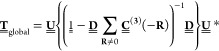 |
17 |
in which  is defined as the matrix
including sub-T-matrices
of every scatterers in the cluster.
is defined as the matrix
including sub-T-matrices
of every scatterers in the cluster.
In this way, the calculation of the response is much more effective and efficient than the quantum-mechanical simulation for multiple objects.
Description of a Thin Film of Clusters of Metallic Molecules
At this stage, we can classically describe the interaction of light with a cluster of metallic molecules placed in silica (SiO2) as the background medium. Now, we wish to describe the reflection and transmission from a thin film of periodically arranged clusters of metallic molecules at a next higher level of aggregation. Please note that at this stage, an assumption enters the description that shall be shortly discussed. Of course, the periodic arrangement of identical clusters will not occur in reality. However, the individual metallic molecules will mostly interact with their nearest neighbors. They will not explicitly interact with particles that are much further away. Therefore, the explicit arrangement on these longer scales will not affect the response, and the periodic arrangement will have no impact. A notable interaction across neighboring unit cells would only be encountered if lattice resonances would have been expected. However, they rather appear for lattices characterized by a period comparable to the wavelength. When compared to these scales, we are still having periods much smaller.
To solve the reflection and transmission from a thin film made from periodically arranged clusters, we solve the multiple scattering problem again but consider now (a) that all the particles are identical and (b) they are perfectly periodically arranged. In this case, we utilize lattice summation techniques for simulation multiscattering of an array of identical scatterers. Using the integral representation of the VSH and the direct application of Poisson’s formula, the scattered field from all lattice points R at normal incidence is37
| 18 |
where  and k∥ is the tangential component of the incoming plane
wave. The infinite
lattice sums are partially evaluated in real space and partially in
reciprocal space to assure convergence.
and k∥ is the tangential component of the incoming plane
wave. The infinite
lattice sums are partially evaluated in real space and partially in
reciprocal space to assure convergence.
At this stage, we can describe classically the reflection and transmission from a slab containing the metallic molecules with a finite thickness. The slab is illuminated by linearly polarized plane-wave propagating in the +z direction and with an amplitude Ẽinc. The vectorial reflection (r) and transmission coefficients (t) can be obtained by transforming the scattered field in eq 18 from the real space to the reciprocal space and using the definition of the coefficients,
| 19 |
Ẽsca, z± implies the vectorial amplitude of the reflected field for the – index and the transmitted field for the + index in reciprocal space if the incident field is considered propagating along the positive z axis. The reflected field comes from the superposition of scattered field in the negative z axis, while the transmitted field is generated in the positive z axis. The linear polarization of the incident field, of course, is preserved for the reflected and transmitted field. Alternatively, the reflection and transmission coefficient also can be directly obtained from expansion coefficients {anm, bnm} from the nanoparticle layer,38 if its T-matrix is known. Then, the reflectance (R) and transmittance (T) for normal incidence can be stated to
| 20 |
The indices {s, c} in eq 20 represent the substrate and cladding in order. The incoming wave travels in the substrate, and the cladding is defined as the second layer parallel to the film. Finally, the absorptance (A) is defined as
| 21 |
Effective Description of a Thin Film of Clusters of Metallic Molecules
At this stage, we can describe classically the reflection and transmission from a slab containing the metallic molecules with a finite thickness. We aim to describe this material using an effective dielectric function to advance toward the next length scale. Using such an effective dielectric function, we can consider the material in designing arbitrary functional devices. In our case, this is the perfect broadband absorber. The huge advantage would be that we can also change the thickness of the slab continuously in the design without being required to consider always a unit cell with a suitable thickness. Since the critical length scale is much smaller than the wavelength, we can treat it as a metamaterial to which we assign effective properties.
While considering reflection and transmission from a slab with a given thickness, corresponding in our case to the size of the cubical unit cell considered as the cluster, we can derive from the complex reflection and transmission coefficients (r, t), the effective electric permittivity (ϵeff), and the effective magnetic permeability (μeff) for a normal linear-polarized plane-wave illumination assuming an isotropic, homogeneous, local medium, without electromagnetic coupling as39,40
| 22 |
| 23 |
where parameters kf and ζf are defined as
| 24 |
and
| 25 |
m is the integer user-chosen branch order to ensure continuity of the wave vector in the respective medium. The parameter J in eqs 24 and 25 is
| 26 |
In our case, the substrate and the cladding are in vacuum medium, so that [ϵs, ϵc, μs, μc] = 1. Therefore, we can treat the material comprising Au144 metallic molecules as a homogeneous material and consider it in the next level of our description.
Optimization of the Actual Perfect Absorber
Finally, a multilayer thin film system is studied to model a device. All materials involved are described at the level of a dielectric function. The Au144 cluster embedded into a SiO2 matrix is deposited on top of a pure SiO2 spacer and gold mirror. By assuming that the sum of reflectance (R), transmittance (T), and absorptance (A) is always unity, a classical thin film transfer matrix method41 is used to calculate the absorptance of the thin film system. Then, the area below the resulting absorption curve is determined and normalized to get the most optimal thin film thickness to get the best broadband absorption. We aim to find the optimal absorption by varying the thickness of the thin film containing the metallic molecules and the spacer layer (dnp, dspacer) by maximizing the objective function over the area below the resulting absorption curve
| 27 |
Taken all aspects together, we have sketched above a computational approach to predict an optimal broadband perfect absorber while starting from the consideration of its constituents within a quantum-chemical description. It is a true multiscale modeling since we start from the electronic details of an individual metallic molecule and go up to a macroscopic device. The thin film thickness may be in the order of 100 nm, but of course, also thicker films could have been considered. This thickness was chosen exemplary for that specific device, other values could be set as well. In the next section, we present the results of the analysis.
Results and Discussion
Properties of an Individual Metallic Molecule
As outlined in the previous section, using the T-matrix obtained from LR-TDDFT, we apply eq 10 to determine the electric polarizability from a Au144 metallic molecule. The results are shown in Figure 2. For the DFT part, we employed the PBE functional42,43 together with the def2-TZVP basis set.44 The def2-TZVP basis set is used in conjunction with an effective core potential (ECP60MWB),45 where 60 electrons are placed inside the ECP. The ECP introduces scalar-relativistic effects, which are, therefore, properly accounted for. Spin-orbit interactions are neglected due to the vast computational effort that would be needed to carry out fully relativistic calculations at the given molecular sizes. Equation 1 was solved using the efficient semi-numerical semiJK algorithm,46 employing fine grids for the Coulomb potential and a grid of size 4 for the exchange-correlation part.47 For the simulations of Au144 embedded in SiO2, a refractive index of 1.46 and an ϵ of 3.90 have been used to simulate the SiO2 surrounding. For the cavity construction, a radius of r = 2.223 bohr was used for Au. All calculations have been performed with a development version of Turbomole V7.6.48
Figure 2.

(a) Magnitude of the electric dipolar polarizability of a Au144 nanoparticle in air and SiO2. (b) Transition density for the plasmonic peak of the Au144 generated from the polarizabilities from 2.0 to 2.5 eV. An isovalue of 0.00015 a.u. was used.
The polarizability curve displayed
in Figure 2a exhibits
several maxima, corresponding
to peaks in light absorption at the frequencies where they occur.
When embedded into a  matrix, a significant shift of the peaks
is observed. Especially the peaks found at λ = 460 nm and λ
= 565 nm are shifted to a longer wavelength compared to vacuum/air.
Also, a distinct increase in the polarizability is observed if the
matrix, a significant shift of the peaks
is observed. Especially the peaks found at λ = 460 nm and λ
= 565 nm are shifted to a longer wavelength compared to vacuum/air.
Also, a distinct increase in the polarizability is observed if the  nanoparticle is embedded in the
  matrix.
The polarizability obtained from DFT is closely connected to standard excited-state TD-DFT. Therefore, similarly, peaks can be analyzed by calculating a transition-density like property. This is done by summing the eigenvectors described in eq 1 and weighting them by the trace of the polarizability tensor. The latter is directly related to the oscillator strength used in standard TD-DFT excited state spectra. The corresponding transition density for the peak starting at above 400 nm in Figure 2a is shown in Figure 2b. The resulting transition density outlines the average charge movement away from the gold atoms in this band. For bulk gold, the corresponding band at 2.2 eV exhibits a distinct plasmonic character, and the charge movement in Figure 2b hints at this excitation also having a significant plasmonic character already. This is in agreement with general findings for small noble metal clusters.49
Properties of a Cluster of Metallic Molecules
As the next target of this study is an ab initio based multiscale modeling approach, we now focus on the effects of the interaction of multiple neighboring Au144 nanoparticles on the optical response. For this purpose, we compare the classically calculated absorption cross section of a Au144 nanoparticle to a cluster comprising a larger number of the nanoparticles. The combined T-matrix for a given number of nanoparticles is obtained and subsequently used to calculate the absorption cross section of the cluster of nanoparticles through eqs 14–16. It turns out that the interaction between the nanoparticles does not induce new resonance peaks in the optical absorption spectrum, as shown in Figure 3. The absorption curves are dominated by the usual scaling in the Rayleigh regime, but subtle underlying features are still affected.
Figure 3.

Absorption cross-section from a single Au144 nanoparticle (left y axis) and a cluster comprising 101 Au144 nanoparticles (right y axis).
Instead, the magnitude of absorption is enhanced. This is the expected effect for gold nanoparticles, which by themselves are only weakly interacting with each other through van der Waals forces. Moreover, since the particles are so small that scattering is negligible, a possible radiative interaction among the metallic molecules is absent. In that sense, the results are consistent with physical expectations. Nevertheless, the effect of interaction is fully considered and accommodated in our approach.
Properties of a Thin Film of Clusters of Metallic Molecules
Next, we consider a periodic arrangement of nanoparticle clusters when assembled into a thin film. We choose air as the surrounding material when considering reflection and transmission from this thin film. The thickness of the layer is the actual domain side length of the cubical cluster of the metallic molecules. We choose here a side length of dnp = 13.9 nm. We also want to study the optical response when considering thin films with different thicknesses. For this purpose, we consider layers comprising a different number of clusters of metallic molecules as previously considered. Figure 4 shows reflectance, transmittance, and absorptance when considering thin films made from 1, 2, or 4 layers, respectively. The thin films have a thickness of L ≈ {13.9,27.8,55.7} nm, respectively. According to Figure 4, the absorptance is getting stronger, and the transmittance becomes weaker as the number of layer stacks increases as expected. Also, all three quantities are strongly affected in the spectral region for which the metallic molecules sustain localized plasmon interaction as mentioned before, i.e., most notably in the spectral region between 400 and 600 nm. Reflectance and transmittance decrease while absorptance enhances.
Figure 4.

(a) Reflectance, (b) transmittance, and (c) absorptance for Au144 nanoparticle thin film stacks depending on the thickness. Please note that the thickness corresponds to an integer multiply of the thickness of the previously considered cluster of metallic molecules.
Using the reflection and transmission coefficient data of the nanoparticle layer, the effective relative electric permittivity of the material made from densely packed Au144 nanoparticles is calculated. Figure 5 shows the real and imaginary parts of the retrieved effective permittivity. The real part of the permittivity is high around λ > 600 nm and the imaginary part of the permittivity has a roughly similar feature to the polarizability curve in Figure 2a. Eventually, the excitation of localized plasmon polaritons in the metallic molecule translates to a Lorentzian resonance in the effective permittivity. The spectral position is best identified from the peaks in the imaginary part. The real part shows the respective dispersion. It attains high values at wavelengths longer than the resonance wavelength, which agrees with common expectations of a Lorentz oscillator. We carefully checked that the number of layer stacks does not change the relative permittivity. We can conclude from this observation that the material can nicely be described at the effective level using a dielectric function as retrieved. A nearly identical dispersion of the effective permittivity that is independent of the thickness of the considered thin film is also an indication that the interface effect between air and the nanoparticle layer has a vanishing impact on the response in these optical considerations. Therefore, the nanoparticle thin film layer is considered homogeneous.
Figure 5.

Real and imaginary parts of the effective relative electric permittivity of the Au144 nanoparticles in SiO2 matrix thin film stacks.
Properties of the Broadband Perfect Absorber
Lastly, we regard a multilayer thin film system to create a broadband perfect absorber. The thin film system, illustrated in Figure 6, consists of a layer comprising the Au144 metallic molecules, considered in the optical simulations as nanoparticles, embedded into a SiO2 matrix, a SiO2 spacer layer, and a semi-infinite gold mirror.
Figure 6.

Scheme of the considered multilayer thin film system.
Realizing such a geometry is entirely feasible with existing technologies. The metallic nanoparticles have to be co-deposited with the dielectric host to make the nanoparticles act as a functional plasmonic material. For example, Vahl et al.50 have demonstrated the fabrication of a thin film containing alloyed metallic nanoparticles in a SiO2 matrix. The metallic nanoparticles were deposited via a Haberland-type gas aggregation cluster source, and the SiO2 was deposited through an RF sputtering method. Both of these materials are continuously deposited, and the SiO2 as a host material builds up as a film with time passing. Details of the nanoparticles deposited with such techniques can be controlled quite flexibly. For example, the filling fraction can be easily controlled by the deposition rates, so that the nanoparticles can be made densely or loosely packed in the dielectric matrix. Also, the deposited nanoparticles do not have any specific spatial arrangement with respect to each other, so the spherical nanoparticles approximation applies here.
The specific thickness of the Au144 nanoparticle layer and the spacer layer is going to be determined to have an optimal broad and strong absorption from UV to visible light region, i.e., from 300 to 800 nm. While considering the material comprising the metallic molecules at the effective level and relying on a transfer matrix method to compute the optical response from a thin film stack, the computations are extremely fast and efficient. With this approach, the area of the absorption curve is obtained for each variation of layer thicknesses within a feasible range, i.e. dnp = 0 – 100 nm and dspacer = 0 – 100 nm. To quantify the broadband absorptance, we integrate it across the relevant spectral domain and normalize it to the absorptance of a perfectly functioning device in the same spectral region. This normalized integrated absorptance is hence a quantity between 0 and 1. The normalized integrated absorptance depending on the thickness of the spacer and the thin film comprising the metallic molecules is shown in Figure 7a. The figure clearly reveals an optimal absorptance for a system made from dnp = 15 nm and dspacer = 39 nm. Figure 7b shows the optical response of the perfect absorber comprising the optimized layer thicknesses. We see that the very high absorption of visible light is key to broadband absorptance in general. At infrared wavelengths, we predict that the overall response gets weaker. This is not surprising considering the weaker plasmonic response of the metallic molecules at these wavelengths.
Figure 7.

(a) Absorption colormap of variation of Au144 nanoparticle thin films and dielectric spacer layer thicknesses. A blue ring points to the optimal nanoparticle layer and spacer layer thickness. (b) Reflectance, transmittance, and absorption curve at optimal thin film layer thicknesses.
Conclusions
We have demonstrated the multiscale modeling of a broadband perfect absorber made from Au144 molecules. It starts with a quantum-chemical analysis of the gold molecules using TDDFT. This analysis provides information on the electric dipole polarizabilities of the metallic molecule that is converted to a T-matrix appropriate for classical optical simulations. Next, a cluster of Au144 is generated to describe the interaction of light between the metallic molecules. Afterward, we periodically arrange these clusters to let them form a thin film from which reflection and transmission are calculated. Inverting these optical coefficients allows for homogenizing the thin film and treating it in subsequent optical simulations as a homogeneous material characterized by a dielectric function. Finally, a broadband perfect absorber device is considered by stacking layers containing metallic molecules, silica, and a semi-infinite gold mirror above each other. Varying the thicknesses of the layers allows for finding a configuration where the absorption is optimal within some predefined spectral region.
The suggested architecture has multiple advantages with respect to other devices designed for a similar purpose. For example, by exploiting the multiple reflections in the thin film layers that lead to a vanishing reflection due to destructive interference, the proposed broadband absorber can be designed to be very thin. When compared to experimentally fabricated metallic broadband absorbers with an equivalent configuration and layer thicknesses,17,51 the absorption curve is analogously almost perfect across the entire visible part of the spectrum. Experimentally, it is also possible to fabricate the ultrathin metallic film on a large scale and in a self-assembly manner, which ultimately implies also rather low costs. This is in contrast to alternative approaches that rely on top-down nanofabrication techniques. Combining all these benefits suggests that more applications can profit from an accessible functionality, well beyond those demonstrated in the current work. For instance, small organic molecules can be considered for photovoltaic devices52 or chiral materials53 can be studied on a macroscopical scale.
We believe that our results can be used as a reference for future design studies of ultrathin perfect absorbers. Compared to our results, the absorption can be stronger at longer wavelengths by considering nanoparticles other than Au144, such as tungsten,54 to cover also the near infra-red absorption spectrum. They could also be arranged denser to increase the interactions between the nanoparticles. The bottom line is that with this methodology, effects in the investigated and related systems occurring on chemical or physical grounds can be simultaneously considered and accurately modeled.
Acknowledgments
C.H. and C.R. acknowledge funding by the Volkswagen Foundation. N.P. and C.R. acknowledge support by the Deutsche Forschungsgemeinschaft (DFG, German Research Foundation) (Project No. 413974664) within Project RO 3640/12-1. The authors acknowledge support by the state of Baden-Württemberg through bwHPC and the German Research Foundation (DFG) through grant no INST 40/575-1 FUGG (JUSTUS 2 cluster).
The authors declare no competing financial interest.
Notes
The Au144 molecular structure and the nanoparticles’ position in Figure 1b (with the nanoparticles having an identical radius of 0.7516 nm) are available in the standard “.xyz” format in Zenodo at DOI: 10.5281/zenodo.6474616.55
References
- Yam C.; Meng L.; Zhang Y.; Chen G. A multiscale quantum mechanics/electromagnetics method for device simulations. Chem. Soc. Rev. 2015, 44, 1763–1776. 10.1039/C4CS00348A. [DOI] [PubMed] [Google Scholar]
- Hollingsworth S.; Dror R. Molecular Dynamics Simulation for All. Neuron 2018, 99, 1129–1143. 10.1016/j.neuron.2018.08.011. [DOI] [PMC free article] [PubMed] [Google Scholar]
- Lubbers N.; Agarwal A.; Chen Y.; Son S.; Mehana M.; Kang Q.; Karra S.; Junghans C.; Germann T.; Viswanathan H. Modeling and scale-bridging using machine learning: nanoconfinement effects in porous media. Sci. Rep. 2020, 10, 13312. 10.1038/s41598-020-69661-0. [DOI] [PMC free article] [PubMed] [Google Scholar]
- Bousige C.; Levitz P.; Coasne B. Bridging scales in disordered porous media by mapping molecular dynamics onto intermittent Brownian motion. Nat. Commun. 2021, 12, 1043. 10.1038/s41467-021-21252-x. [DOI] [PMC free article] [PubMed] [Google Scholar]
- Berghoff M.; Nestler B. Scale-bridging phase-field simulations of microstructure responses on nucleation in metals and colloids. Eur. Phys. J.: Spec. Top. 2014, 223, 409–419. 10.1140/epjst/e2014-02099-8. [DOI] [Google Scholar]
- Lim H.; Abdeljawad F.; Owen S.; Hanks B.; Foulk J.; Battaile C. Incorporating physically-based microstructures in materials modeling: Bridging phase field and crystal plasticity frameworks. Modell. Simul. Mater. Sci. Eng. 2016, 24, 045016 10.1088/0965-0393/24/4/045016. [DOI] [Google Scholar]
- Geelen R.; Plews J.; Dolbow J. Scale-bridging with the extended/generalized finite element method for linear elastodynamics. Comput. Mech. 2021, 68, 295–310. 10.1007/s00466-021-02032-2. [DOI] [Google Scholar]
- Lin W.; Insley T.; Tuttle M.D.; Zhu L.; Berthold D.A.; Král P.; Rienstra C.M.; Murphy C.J. Control of Protein Orientation on Gold Nanoparticles. J. Phys. Chem. C 2015, 119, 21035–21043. 10.1021/acs.jpcc.5b07701. [DOI] [PMC free article] [PubMed] [Google Scholar]
- Rademacher M.; Millen J.; Li Y.L. Quantum sensing with nanoparticles for gravimetry: when bigger is better. Adv. Opt. Technol. 2020, 9, 227–239. 10.1515/aot-2020-0019. [DOI] [Google Scholar]
- Wang Y.; Bao L.; Liu Z.; Pang D.W. Aptamer biosensor based on fluorescence resonance energy transfer from upconverting phosphors to carbon nanoparticles for thrombin detection in human plasma. Anal. Chem. 2011, 83, 8130–8137. 10.1021/ac201631b. [DOI] [PubMed] [Google Scholar]
- Huang J.; Xie Z.; Xie Z.; Luo S.; Xie L.; Huang L.; Fan Q.; Zhang Y.; Wang S.; Zeng T. Silver nanoparticles coated graphene electrochemical sensor for the ultrasensitive analysis of avian influenza virus H7. Anal. Chim. Acta 2016, 913, 121–127. 10.1016/j.aca.2016.01.050. [DOI] [PubMed] [Google Scholar]
- Wu S.; Li D.; Wang J.; Zhao Y.; Dong S.; Wang X. Gold nanoparticles dissolution based colorimetric method for highly sensitive detection of organophosphate pesticides. Sens. Actuators, B 2017, 238, 427–433. 10.1016/j.snb.2016.07.067. [DOI] [Google Scholar]
- Quesada-González D.; Jairo G.A.; Blake R.C. II; Blake D.A.; Merkoçi A. Uranium (VI) detection in groundwater using a gold nanoparticle/paper-based lateral flow device. Sci. Rep. 2018, 8, 16157. 10.1038/s41598-018-34610-5. [DOI] [PMC free article] [PubMed] [Google Scholar]
- Bordo V.G. Quantum light from a metal nanoparticle. Phys. Rev. A 2019, 100, 063807. 10.1103/PhysRevA.100.063807. [DOI] [Google Scholar]
- Baron A.; Aradian A.; Ponsinet V.; Barois P. Self-assembled optical metamaterials. Opt. Laser Technol. 2016, 82, 94–100. 10.1016/j.optlastec.2016.02.024. [DOI] [Google Scholar]
- Bonin G.O.; Barrow S.J.; Connell T.U.; Roberts A.; Chesman A.S.R.; Gómez D.E. Self-Assembly of Plasmonic Near-Perfect Absorbers of Light: The Effect of Particle Size. J. Phys. Chem. Lett. 2020, 11, 8378–8385. 10.1021/acs.jpclett.0c02461. [DOI] [PubMed] [Google Scholar]
- Hedayati M.K.; Javaherirahim M.; Mozooni B.; Abdelaziz R.; Tavassolizadeh A.; Chakravadhanula V.S.K.; Zaporojtchenko V.; Strunkus T.; Faupel F.; Elbahri M. Design of a perfect black absorber at visible frequencies using plasmonic metamaterials. Adv. Mater. 2011, 23, 5410–5414. 10.1002/adma.201102646. [DOI] [PubMed] [Google Scholar]
- Hedayati M.K.; Zillohu A.U.; Strunskus T.; Faupel F.; Elbahri M. Plasmonic tunable metamaterial absorber as ultraviolet protection film. Appl. Phys. Lett. 2014, 104, 041103. 10.1063/1.4863202. [DOI] [Google Scholar]
- Ghori M.Z.; Veziroglu S.; Hinz A.; Shurtleff B.B.; Polonskyi O.; Strunskus T.; Adam J.; Faupel F.; Aktas O.C. Role of UV Plasmonics in the Photocatalytic Performance of TiO2 Decorated with Aluminum Nanoparticles. ACS Appl. Nano Mater. 2018, 1, 3760–3764. 10.1021/acsanm.8b00853. [DOI] [Google Scholar]
- Kats M.A.; Sharma D.; Lin J.; Genevet P.; Blanchard R.; Yang Z.; Qazilbash M.M.; Basov D.N.; Ramanathan S.; Capasso F. Ultra-thin perfect absorber employing a tunable phase change material. Appl. Phys. Lett. 2012, 101, 221101. 10.1063/1.4767646. [DOI] [Google Scholar]
- Sun J.; Liu L.; Dong G.; Zhou J. An extremely broad band metamaterial absorber based on destructive interference. Opt. Express 2011, 19, 21155–21162. 10.1364/OE.19.021155. [DOI] [PubMed] [Google Scholar]
- Henninen T.R.; Bon M.; Wang F.; Passerone D.; Erni R. The Structure of Subnm Platinum Clusters at Elevated Temperatures. Angew. Chem., Int. Ed. 2020, 59, 839–845. 10.1002/anie.201911068. [DOI] [PubMed] [Google Scholar]
- Kraft M.; Flores J.R.; Klopper W.; Kappes M.M.; Schooss D. Structures of Small Tantalum Cluster Anions: Experiment and Theory. J. Phys. Chem. A 2021, 125, 3135–3145. 10.1021/acs.jpca.1c01250. [DOI] [PubMed] [Google Scholar]
- Pal R.; Poddar A.; Chattaraj P.K. Atomic Clusters: Structure, Reactivity, Bonding, and Dynamics. Front. Chem. 2021, 9, 730548. 10.3389/fchem.2021.730548. [DOI] [PMC free article] [PubMed] [Google Scholar]
- Jensen K.M.Ø.; Juhas P.; Tofanelli M.A.; Heinecke C.L.; Vaughan G.; Ackerson C.J.; Billinge S.J.L. Polymorphism in magic-sized Au144(SR)60 clusters. Nat. Commun. 2016, 7, 11859. 10.1038/ncomms11859. [DOI] [PMC free article] [PubMed] [Google Scholar]
- Yan N.; Xia N.; Liao L.; Zhu M.; Jin F.; Jin R.; Wu Z. Unraveling the long-pursued Au144 structure by x-ray crystallography. Sci. Adv. 2018, 4, eaat7259. 10.1126/sciadv.aat7259. [DOI] [PMC free article] [PubMed] [Google Scholar]
- Senanayake R.D.; Lingerfelt D.B.; Kuda-Singappulige G.U.; Li X.; Aikens C.M. Real-Time TDDFT Investigation of Optical Absorption in Gold Nanowires. J. Phys. Chem. C 2019, 123, 14734–14745. 10.1021/acs.jpcc.9b00296. [DOI] [Google Scholar]
- Fernandez-Corbaton I.; Beutel D.; Rockstuhl C.; Pausch A.; Klopper W. Computation of Electromagnetic Properties of Molecular Ensembles. ChemPhysChem 2020, 21, 878–887. 10.1002/cphc.202000072. [DOI] [PMC free article] [PubMed] [Google Scholar]
- Bauernschmitt R.; Ahlrichs R. Treatment of electronic excitations within the adiabatic approximation of time dependent density functional theory. Chem. Phys. Lett. 1996, 256, 454–464. 10.1016/0009-2614(96)00440-X. [DOI] [Google Scholar]
- Furche F. On the density matrix based approach to time-dependent density functional response theory. J. Chem. Phys. 2001, 114, 5982–5992. 10.1063/1.1353585. [DOI] [Google Scholar]
- Kehry M.; Franzke Y.J.; Holzer C.; Klopper W. Quasirelativistic two-component core excitations and polarisabilities from a damped-response formulation of the Bethe– Salpeter equation. Mol. Phys. 2020, 118, e1755064 10.1080/00268976.2020.1755064. [DOI] [Google Scholar]
- Klamt A. The COSMO and COSMO-RS solvation models. Wiley Interdiscip. Rev.: Comput. Mol. Sci. 2011, 1, 699–709. 10.1002/wcms.56. [DOI] [Google Scholar]
- Karbalaei Khani S.; Marefat Khah A.; Hättig C. COSMO-RI-ADC(2) excitation energies and excited state gradients. Phys. Chem. Chem. Phys. 2018, 20, 16354–16363. 10.1039/C8CP00643A. [DOI] [PubMed] [Google Scholar]
- Franzke Y.J.; Holzer C.; Mack F. NMR Coupling Constants Based on the Bethe– Salpeter Equation in the GW Approximation. J. Chem. Theory Comput. 2022, 18, 1030–1045. 10.1021/acs.jctc.1c00999. [DOI] [PubMed] [Google Scholar]
- Mishchenko M. I.; Travis L. D.; Lacis A. A.. Scattering, Absorption, and Emission of Light by Small Particles; Cambridge University Press: Cambridge, 2002. [Google Scholar]
- Baranau V.; Tallarek U. Random-close packing limits for monodisperse and polydisperse hard spheres. Soft Matter 2014, 10, 3826–3841. 10.1039/c3sm52959b. [DOI] [PubMed] [Google Scholar]
- Beutel D.; Groner A.; Rockstuhl C.; Fernandez-Corbaton I. Efficient simulation of biperiodic, layered structures based on the T-matrix method. J. Opt. Soc. Am. B 2021, 38, 1782–1791. 10.1364/JOSAB.419645. [DOI] [Google Scholar]
- Dezert R.; Richetti P.; Baron A. Complete multipolar description of reflection and transmission across a metasurface for perfect absorption of light. Opt. Express 2019, 27, 26317–26330. 10.1364/OE.27.026317. [DOI] [PubMed] [Google Scholar]
- Menzel C.; Rockstuhl C.; Paul T.; Lederer F.; Pertsch T. Retrieving effective parameters for metamaterials at oblique incidence. Phys. Rev. B 2008, 77, 195328. 10.1103/PhysRevB.77.195328. [DOI] [Google Scholar]
- Menzel C.; Paul T.; Rockstuhl C.; Pertsch T.; Tretyakov S.; Lederer F. Validity of effective material parameters for optical fishnet metamaterials. Phys. Rev. B 2010, 81, 035320 10.1103/PhysRevB.81.035320. [DOI] [Google Scholar]
- Mackay T. G.; Lakhtakia A.. The Transfer-Matrix Method in Electromagnetics and Optics; Morgan & Claypool Publishers, 2020. [Google Scholar]
- Perdew J.P.; Burke K.; Ernzerhof M. Generalized Gradient Approximation Made Simple. Phys. Rev. Lett. 1996, 77, 3865–3868. 10.1103/PhysRevLett.77.3865. [DOI] [PubMed] [Google Scholar]
- Perdew J.P.; Burke K.; Ernzerhof M. Generalized Gradient Approximation Made Simple. Phys. Rev. Lett. 1997, 78, 1396–1396. 10.1103/PhysRevLett.78.1396. [DOI] [PubMed] [Google Scholar]
- Weigend F.; Furche F.; Ahlrichs R. Gaussian basis sets of quadruple zeta valence quality for atoms H–Kr. J. Chem. Phys. 2003, 119, 12753–12762. 10.1063/1.1627293. [DOI] [Google Scholar]
- Andrae D.; Haeussermann U.; Dolg M.; Stoll H.; Preuss H. Energy-adjustedab initio pseudopotentials for the second and third row transition elements. Theor. Chim. Acta 1990, 77, 123–141. 10.1007/BF01114537. [DOI] [Google Scholar]
- Holzer C. An improved seminumerical Coulomb and exchange algorithm for properties and excited states in modern density functional theory. J. Chem. Phys. 2020, 153, 184115. 10.1063/5.0022755. [DOI] [PubMed] [Google Scholar]
- Treutler O.; Ahlrichs R. Efficient molecular numerical integration schemes. J. Chem. Phys. 1995, 102, 346–354. 10.1063/1.469408. [DOI] [Google Scholar]
- Balasubramani S.G.; Chen G.P.; Coriani S.; Diedenhofen M.; Frank M.S.; Franzke Y.J.; Furche F.; Grotjahn R.; Harding M.E.; Hättig C.; Hellweg A. TURBOMOLE: Modular program suite for ab initio quantum-chemical and condensed-matter simulations. J. Chem. Phys. 2020, 152, 184107. 10.1063/5.0004635. [DOI] [PMC free article] [PubMed] [Google Scholar]
- Bursi L.; Calzolari A.; Corni S.; Molinari E. Quantifying the Plasmonic Character of Optical Excitations in Nanostructures. ACS Photonics 2016, 3, 520–525. 10.1021/acsphotonics.5b00688. [DOI] [Google Scholar]
- Vahl A.; Strobel J.; Reichstein W.; Polonskyi O.; Strunskus T.; Kienle L.; Faupel F. Single target sputter deposition of alloy nanoparticles with adjustable composition via a gas aggregation cluster source. Nanotechnology 2017, 28, 175703. 10.1088/1361-6528/aa66ef. [DOI] [PubMed] [Google Scholar]
- Hedayati M.K.; Faupel F.; Elbahri M. Tunable broadband plasmonic perfect absorber at visible frequency. Appl. Phys. A 2012, 109, 769–773. 10.1007/s00339-012-7344-1. [DOI] [Google Scholar]
- He X.; Yin L.; Li Y. Design of organic small molecules for photovoltaic application with high open-circuit voltage (Voc). J. Mater. Chem. C 2019, 7, 2487–2521. 10.1039/C8TC06589F. [DOI] [Google Scholar]
- Mun J.; Kim M.; Yang Y.; Badloe T.; Ni J.; Chen Y.; Qiu C.-W.; Rho J. Electromagnetic chirality: from fundamentals to nontraditional chiroptical phenomena. Light: Sci. Appl. 2020, 9, 139. 10.1038/s41377-020-00367-8. [DOI] [PMC free article] [PubMed] [Google Scholar]
- Andersen J.; Bonderup E.; Hansen K. Thermionic emission from clusters. J. Phys. B: At., Mol. Opt. Phys. 2002, 35, R1–R30. [Google Scholar]
- Perdana N.; Holzer C.; Rockstuhl C.. Multiscale modeling of broadband perfect absorbers based on gold metallic molecules - Supporting Information; 2022. [DOI] [PMC free article] [PubMed]