Abstract
Photonic integrated circuits (PICs) for next-generation optical communication interconnects and all-optical signal processing require efficient (∼A/W) and fast (≥25 Gbs–1) light detection at low (<pJbit–1) power consumption, in devices compatible with Si processing, so that the monolithic integration of electro-optical materials and electronics can be achieved consistently at the wafer scale. Graphene-based photodetectors can meet these criteria, thanks to their broadband absorption, ultra-high mobility, ultra-fast electron interactions, and strong photothermoelectric effect. High responsivities (∼ 1 A/W), however, have only been demonstrated in biased configurations, which introduce dark current, noise, and power consumption, while unbiased schemes, with low noise and zero consumption, have remained in the ∼ 0.1 A/W regime. Here, we consider the unbiased asymmetric configuration and show that optimized plasmonic enhanced devices can reach for both transverse-electric and transverse-magnetic modes (at λ = 1550 nm), ∼A/W responsivity, and ∼ 100 GHz operation speed at zero power consumption. We validate the model and material parameters by simulating experimental devices and derive analytical expressions for the responsivity. Our comprehensive modeling paves the way for efficient, fast, and versatile optical detection in PICs with zero power consumption.
Keywords: graphene, photodetectors, integrated photonics, plasmonics, photothermoelectric effect
Introduction
Photonic integrated circuits (PIC)1 can be used for interconnects,2,3 all-optical signal processing,4,5 as well as for neuromorphic photonics,6−8 whereby programmable (trainable) PICs become the photonic hardware counterpart for artificial neural network algorithms. There has been continuous progress in all key performance metrics,9 including increased bandwidth (BW),10 reduced footprint,10 and reduced power consumption,10 with current transceiver technologies already allowing for 400 Gb/s operation,3 and moving towards 800 Gbs–1 9 and 1.6 Tbs–1 interconnect applications.2
With receiver circuitry forming a critical element in the landscape of PICs, this performance race confronts the photodetector (PD) technology with a challenging functionality framework. PDs must constantly aim for smaller-size layouts with high optoelectronic BW (>100 GHz)11 and improved efficiencies (∼ 1 A/W),12,13 while expanding along a complementary metal-oxide-semiconductor (CMOS) process compatible framework.14 At the same time, they are required to operate at a low energy envelope, with improved noise characteristics,10 thus making a strong case for unbiased operational schemes which have zero power consumption, zero dark current, and low noise.15 They also need to support dynamic tunability in both photoresponse and electrical resistance, when their employment in balanced-PD schemes is targeted, i.e. paired PDs of equal response with their signal subtracted to reduce the light source noise,16−18 or subtraction of mixed signals in coherent detection schemes.19 Currently used bulk semiconductor technologies such as Ge20,21 and InP22,23-based PDs cannot meet all these criteria simultaneously. Besides spectral limitations associated with the semiconductor band gap,24 they often enforce process changes20,21,24,25 or experience speed limitations due to the material intrinsic mobility and increased thickness of the photoactive layer.26 These factors led to PD devices with increased complexity,26 and a trade-off between operation speed and responsivity.27
Single-layer graphene (SLG) is ideally suited to meet the abovementioned requirements,10,15,28−30 and a variety of integrated graphene PD (GPDs) prototypes have been demonstrated.31−45 SLG exhibits ultrafast electron interactions (<50 fs),46 extremely high room temperature (RT) carrier mobilities (>10,000 cm2/Vs),47−51 CMOS compatibility,15,52,53 field-effect gate tunability,54−57 and broadband optical response.28,29,58,59 On-Chip GPDs have been reported in both biased31,34,36,40−42,45 and unbiased34−40,44 schemes, demonstrating external responsivity (i.e. ratio of photocurrent Iph to incoming power Pin) up to RI,ext ∼ 0.7 A/W42 and ∼ 0.11 A/W,44 respectively, at ∼ 100 Gb–1.31,41,45 In a biased scheme, a source–drain voltage is applied to SLG and the photocurrent is measured as the difference between bright (under illumination) and dark currents,31 where the bright current is modulated as a result of photoconductive36,60 and photobolometric31,60 effects. Under bias, however, the SLG gapless nature61 leads to a sizable dark current and increased noise,15 resulting in a non-negligible power budget for PD operation (∼ 1 mW)31 and for the overall power requirements.15 Lower power metrics, on the other hand, can be accomplished when PDs operate without bias15,28 exploiting the photothermoelectric (PTE) effect,28,30 whereby an electronic temperature, Te, gradient gives rise to a photovoltage due to the Seebeck effect.62 To get a net photoresponse from the device, the symmetry between source and drain contacts must be broken. This can be achieved by either an architecture supporting asymmetric light absorption,33−35 or by an asymmetric gate creating a lateral pn-junction configuration.36−40,44
Unbiased GPDs reported so far have been typically augmented with absorption enhancement mechanisms to increase the SLG absorption above the 2.3%58 it has when suspended and even lower on a substrate,63 exploiting either photonic crystals40 or plasmonics.32,37,41 However, thus far, RI,ext ≲ 0.11 A/W for unbiased devices,34,36,40,44 significantly lower than the ∼ 0.7 A/W reported for biased GPDs.42 Given the preference for zero dark current, low noise, and low power consumption in PIC PDs, the critical question, then, is whether RI,ext ∼ 1 A/W or above can be obtained in unbiased GPDs.
Here, we show that this is possible, by analyzing the performance of a device architecture consisting of unbiased source–drain contacts asymmetrically placed with respect to a Si waveguide (WG).33−35 We employ coupled optical, thermal, and electrical simulations, and show that the simplest design enables strong (i.e., RI,ext ∼ 1 A/W) performance even at zero bias. We provide realistic full device model and material parameters, validated by comparison to experimental results. This allows us to understand the photoresponse mechanisms, the reasons why prior art reached different results and smaller performance, and how to optimize device concepts and designs (i.e., plasmonic effects at the contact edge, WG and contact configurations, and gating profile). An analytical expression derived for the ideal PTE performance (where absorption occurs only in SLG within a delta distribution at the contact edge without metal losses) defines an ideal internal responsivity (i.e., the ratio of photocurrent Iph to absorbed power Pabs) limit up to few A/W for asymmetric-contact unbiased GPDs. We consider both transverse electric (TE) and transverse magnetic (TM) guided modes. A scan of different gating combinations shows that independent dynamic control of resistance and RI,ext can be achieved, paving the way to balanced photodetection schemes.16−18 Noise, sensitivity, and operation speed metrics are also calculated.
Our comprehensive theoretical framework provides the understanding and guidelines needed to have tunable integrated GPDs with zero-consumption, low-noise, high-sensitivity, and high-speed operation.
Results and Discussion
We consider an integrated GPD comprising a Si WG (220 nm thick) on a silicon-on-insulator substrate, as shown in Figure 1. hBN encapsulation ensures high-mobility SLG at RT.64 Two Au electrodes (100 nm thick) are located asymmetrically on opposite sides of the Si WG to collect the photocurrent assuming unbiased operation: one of them 700 nm off the WG edge, and the other at a distance d, varied between 300 and −100 nm. Two contact formats are explored: 1d edge contact65,66 (Figure 1b) and 2d top contact66,67 (Figure 1c). Three Si WG configurations are also explored: fully embedded34 (Figure 1d), half-embedded35 (Figure 1e), and exposed (Figure 1f). The WG width, w, and device length, L, are varied, while all other parameters in Figure 1 remain fixed.
Figure 1.
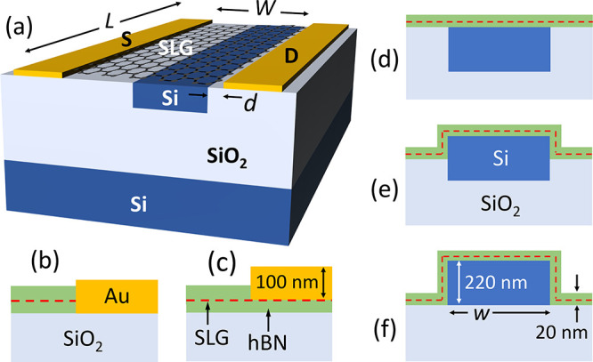
(a) Schematic device configuration with Si WG (220 nm thick) fully embedded in the SiO2 substrate (the encapsulating hBN layers are not shown for clarity). (b,c) Schematic 1d (edge) and 2d (top) contacts, respectively. (d–f) Schematics of 3 WG configurations: fully embedded in SiO2, half embedded, and fully exposed, respectively.
In unbiased metal/GPD devices, both PTE34,68,69 and photovoltaic68−71 mechanisms contribute to the photoresponse, depending on contact metals72,73 and light polarization.69,72 In an asymmetric device configuration, like that studied here, photocurrent measurements as a function of top-gate and source–drain voltages indicated PTE as the dominant effect.34 Thus, we also assume it to be the dominant mechanism here. Its traits include ultrafast detection36,39 and zero-bias operation,15,28,74,75 the latter providing for low noise10,15 and low power consumption.10,15 The PTE effect generates a voltage drop (thus an internal field) VPTE ∝ s∇Te,72,74 where the Seebeck coefficient, s, depends on Te and Fermi level, EF, across the SLG channel, with no requirement of a source–drain bias to observe an ultrafast response.34,35,37,39 For obtaining a net nonzero VPTE without bias, an asymmetry must be present in s(x) or in ∇Te(x), where x runs from source to drain. The former can be achieved by a split-gate to create an in-plane pn-junction.36−40,44 The latter, simpler and employed here, is achieved by asymmetrically positioning the contacts with respect to the Si WG.33−35
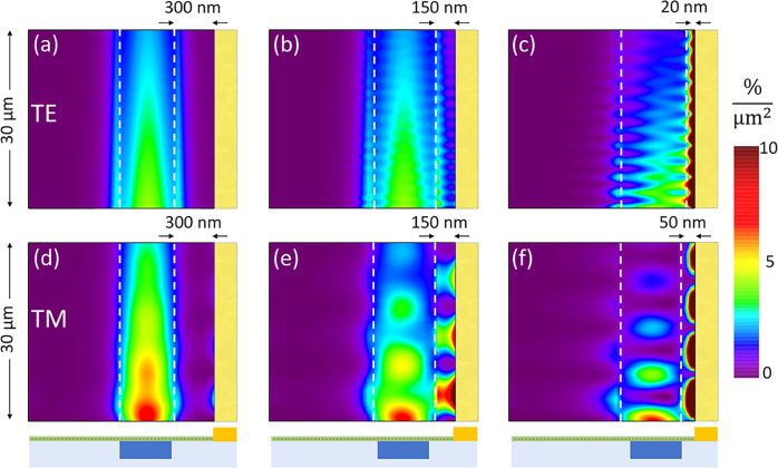
Full-wave simulations, for both the fundamental TE and TM modes at λ = 1550 nm, incident from the Si WG into the PD, in Figure 2, show the emerging optical effects as one of the contacts is brought closer to the WG. The optical mode excites and hybridizes with surface plasmon polaritons (SPP) on the Au contact edge,33 increasing the local SLG absorption. The hybridization is seen by the beating pattern of the absorption along the WG, becoming more pronounced as d decreases, and creating a strong asymmetry in the SLG absorption profile. This increases Te locally, while close to the other contact SLG remains cold. Note, however, that roughness on the metal contact will add to scattering and propagation losses on the plasmon mode, reducing SLG absorption, thus limiting the benefits coming from the SPPs.
Figure 2.
Absorption density αden (%/μm2) in SLG channel for (a–c) TE and (d–f) TM mode at λ = 1550 nm, at different d. The other contact is 700 nm to the left of the figures (not shown). The device configuration is 1d contact, w = 450 nm, L = 30 μm, and fully embedded Si WG. The white dashed lines indicate the Si WG position and the yellow bar the Au contact.
The SLG electron (e) heating and cooling dynamics can be
understood
as follows: light absorption creates hot nonequilibrium carriers which
undergo carrier multiplication by electron–electron (e–e)
scattering (τe–e < 50 fs),46,76,77 i.e., by impact ionization (interband
scattering creating new e-h pairs78,79) and impact
excitation (intraband scattering distributing the excess energy within
the band80) and relax into a hot equilibrium
Fermi–Dirac carrier distribution at an elevated temperature Te.46,76,77,81,82 This hot thermalized carrier distribution is established locally
with one temperature (Te) and chemical
potential (μ).46,77 Local cooling of the e gas then
follows, by electronic heat diffusion and electron–phonon (e–ph)
scattering (τC ∼ 2–4 ps).46,82−89 Due to the much smaller SLG electronic heat capacity compared to
the ones of SLG lattice, hBN, and metal contacts,90 the latter are assumed to remain at RT. Also, plasmonic
hot carrier (HC) effects91,92 in the Au contacts
have a small effect on the PTE response (see Methods). Considering all this, heat diffusion simulations (see Methods) show that the absorption spatial asymmetry
results in a Te asymmetric profile, which,
in turn, gives rise to a thermoelectric voltage74 , where the integration is over the entire
SLG area (length L and width W). VPTE is the device’s open-circuit voltage.
The performance metric is the voltage external responsivity RV,ext = VPTE/Pin, where Pin is
the incoming optical power. If the device internal resistance is RD, then the external sort-circuit current responsivity
is RI,ext = RV,ext/RD. We note that in either open-circuit
or sort-circuit conditions, the output power efficiency of the device
is zero. We now consider the effects of WG, contacts, device geometries,
and SLG doping to reach a generalized understanding of the PTE effects
in integrated GPDs and, by that, an optimization framework.
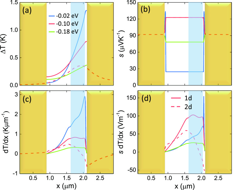
We first examine the SLG EF effect. We assume it pinned at −0.15 eV at/under the contacts (because of charge flow between SLG and metal reaching an equilibration depending on the metal work function),93 while it can vary across the channel (source-to-drain). Typically, SLG is found to be p-doped.94 We consider 3 indicative EF = −0.02, −0.10, −0.18 eV, corresponding to extremely low, low, and average doping for hBN encapsulated SLG, respectively.95,96Figure 3a plots the distribution of Te increase within the SLG channel for a d = 50 nm and L = 30 μm device illuminated with TE polarization at 1 μW. The absorption profile is practically the same for any EF in the range −0.21 to 0.21 eV, but differences in heat capacity and thermal conductivity (see Methods) result in different Te profiles. In addition, the different EF gives different s (see Methods). As shown in Figure 3c,d, the profile and peak position of the thermoelectric voltage are determined by the Te gradient, while s determines the magnitude. Thus, while EF = −0.10 eV does not produce the largest Te gradient (see Figure 3c), it does yield the largest thermoelectric voltage due to the larger s, as for Figure 3b.
Figure 3.
Spatial distribution of thermal quantities across SLG channel at the front (entrance) of the device for 1 μW incoming power with d = 50 nm, L = 30 μm, TE polarization, and fully embedded Si WG configuration. Solid lines correspond to various SLG EF for a 1d contact, while the dashed line corresponds to EF = −0.1 eV for a 2d contact. EF is assumed fixed at −0.15 eV under the contacts. (a) Te increase, (b) s, (c) Te gradient, and (d) local thermoelectric voltage s∇Te projected along the x (source–drain) direction. In all panels, the yellow bars indicate the Au contacts, and shaded light blue the Si WG.
The main difference between 1d and 2d contacts is that in the latter SLG extends under them,66 providing extra space for cooling through electronic heat diffusion and e–ph scattering. In the 1d case, in contrast, the electronic heat diffusion process is terminated at the contact edge, which results in a larger Te gradient, thus higher RI,ext. Cooling can be faster (i.e., smaller τC) locally where SLG is directly contacted by Au97,98 (due to interactions with Au’s e and ph or due to resonant dissipation from atomic defects along the SLG edges99). This affects the performance of both 1d and 2d contacts. We will start by assuming τC to be everywhere the same, so to derive an upper limit for the performance, then consider the effects of faster cooling at the contacts.
To systematically optimize d and EF, we continuously vary them within the range −100 nm < d < 300 nm and −0.21 eV < EF < 0.21 eV. The unbiased RI,ext is plotted in Figure 4 for both polarizations (TE and TM) and both contact geometries (1d and 2d) for the fully embedded Si WG configuration. 1d is better than 2d in all the parameter space. RI,ext increases as d is reduced, reaching an optimum at d = 20 nm and d = 50 nm for TE and TM polarizations, respectively (see Figure 2c,f), where the best compromise between plasmonic field confinement and losses is achieved (see Figure 4 and Methods). If the contact gets closer than this optimal d or overlaps with the WG (i.e., d < 0), RI,ext drops sharply due to increased metal absorption and scattering of the mode on the Au contact edge (see Methods). We note that ref (100) presented the case of complete overlap between contact and underlying WG (i.e., d < −450 nm), reporting RI,ext ∼ A/W as a result of optimistic SLG property values (i.e., heat capacity ce ∼150 J m–3 K–1 and cooling time τC ∼ 10 ps; thus interfacial heat conductance Γcool = ce/τC ∼ 5 × 10³ W m–2 K–1 ∼ 10 times smaller than our ∼5 × 10⁴ W m–2 K–1, and also zero contact resistance). Indeed, simulating the ref (100) structure using their parameters we reproduce their findings, but with our SLG property assumptions, we obtain RI,ext < 0.1 A/W, which is in line with Figure 4. We stress that the use of improper SLG parameters can lead to erroneously inflated responsivities, e.g, ∼ 1000 A/W in ref (101) (here τC ∼ 5 ns was used, instead of the experimentally measured τC ∼ 3 ps,46,82−89 and zero contact resistance). For TM, the response is less sensitive to d, due to the more extended fields and stronger coupling with the Au SPPs, as evident in Figure 2. For both cases, the optimal EF = ±0.07 eV. This is the optimal point of two counter-acting trends: at smaller EF, s drops sharply. At larger EF, thermal conductivity and thermal capacity increase (see Methods) resulting in reduced Te gradients.
Figure 4.
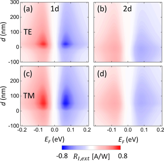
RI,ext [A/W] as a function of SLG EF and d for (a,b) TE and (c,d) TM modes. (a,c) 1d and (b,d) 2d contacts. Calculations are for fully embedded Si WG, with w = 450 nm and L = 30 μm.
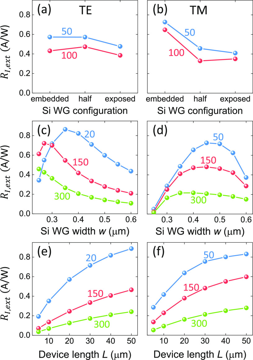
We now consider the 1d contacts, EF = −0.07 eV, and perform optimization simulation runs, shown in Figure 5 for both TE and TM polarizations. The effect of Si WG position with respect to the top oxide surface is shown in Figure 5a,b for two d. The fully embedded configuration is the optimal one for both polarizations. This is also easier to fabricate because the device is on a flat substrate. In Figure 5c,d, the effect of w is studied, assuming the fully embedded configuration. Different trends are observed between the two polarizations. For the optimal d = 20 and 50 nm for TE and TM, the peak RI,ext is observed at w = 350 and 450 nm, respectively. Narrowing the WG width results in vanishing RI,ext for TM, but not for TE. In both cases, detuning from the optimal w degrades RI,ext. A wider WG spreads out the mode, and a narrower WG reduces mode confinement, both cases resulting in smaller Te gradients.
Figure 5.
RI,ext (A/W) for SLG EF = −0.07 eV at 1d contact configuration, as a function of (a,b) WG embedding (at L = 30 μm and w = 450 nm), (c,d) w (fully embedded Si WG and L = 30 μm), (e,f) L (fully embedded Si WG and w = 450 nm). The numbers on the curves indicate different d. Panels (a,c,e) are for TE and (b,d,f) for TM mode.
Figure 5e,f shows the effect of device length. The trends in TE and TM polarizations are very similar, with a monotonic RI,ext increase for longer devices. This is due to larger overall absorption and smaller SLG channel resistance. An opposite trend is observed for the external voltage responsivity RV,ext (i.e., photovoltage Vph to incoming power Pin(30)), where the higher absorption density in the device entrance promotes a larger RV,ext for shorter devices (see Methods).
The dependence of PTE response on SLG EF opens a new avenue for dynamic control of both resistance and responsivity, towards a balanced photodetection scheme.16−19 This is an established method to reduce the effect of intrinsic light-source noise.16 A simple embodiment is realized by two PDs of equal RI,ext, whereby subtraction of their photocurrents removes the excess noise.16 The balanced PD pair output remains zero until a signal difference causes an “unbalance”, thus a net output.16 Balanced PDs are also essential in coherent detection schemes.19 which can significantly increase the transmission capacity by using the phase, amplitude, and polarization of the optical signal to carry information.
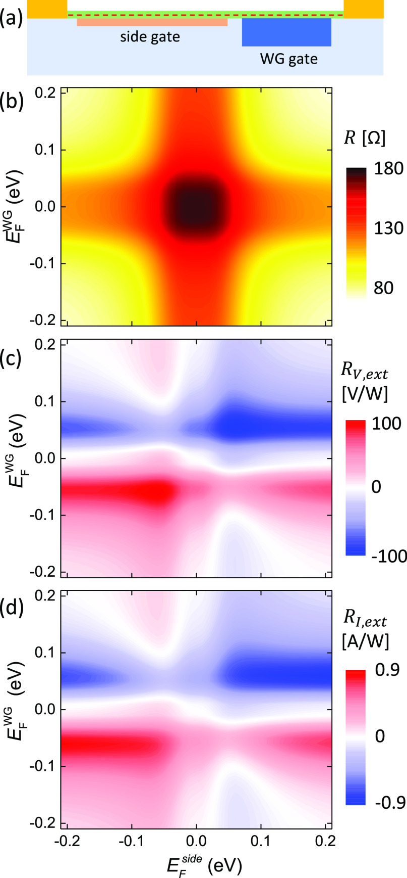
Figure 6a shows a schematic concept in which the Si WG is used as a gate, and a secondary gate is inserted on the side (we assume it does not affect the optical mode or the SLG absorption profile). The device has L = 30 μm, 1d contact layout, fully embedded WG, w = 450 nm, and d = 20 nm, at TE polarization. The device resistance RD as a function of WG and side SLG EF is in Figure 6b, while the corresponding RV,ext and RI,ext are in Figure 6c,d, respectively. Under these assumptions (see Methods), RD = 130 ± 50 Ω (∼ ± 40% change) as VG varies. A sixfold pattern emerges, typical of PTE,62 with values ranging between 0 and ∼100 V/W or 0 and ∼0.9 A/W for RV,ext and RI,ext, respectively. RV,ext increases further for shorter L, as shown in Methods, where it can exceed 200 V/W.
Figure 6.
(a) Schematic double-gating architecture, employing a WG gate and a side gate. (b) Resistance, (c) RV,ext [V/W], and (d) RI,ext [A/W] as a function of SLG “WG” and “side” EF, for the TE mode, d = 20 nm, L = 30 μm, w = 450 nm, 1d contact and fully embedded Si WG.
The operational optimal is at EFWG = EF = ±0.06 eV for RV,ext, reaching up to 102 V/W, but at EFWG = ±0.06 eV, EF = ±0.2 eV for RI,ext, reaching up to 0.88 A/W. The reason is as follows: the SLG EF above the WG (where the highest Te gradients are found) needs to be EFWG = ±0.06 eV. Increasing the side |EF| > 0.06 eV results in s reduction, as well as electrical resistance reduction (see Methods). This translates into a reduced (because of s) thermoelectric voltage (RV,ext reduction), but with a marginally increased (because of resistance) thermoelectric current (RI,ext increase). In either case, the independent variation of EF and EFside can enable independent dynamic control of RD, and RV,ext, towards balanced photodetection.
RV,ext and RI,ext assume open-circuit and short-circuit conditions, respectively,i.e., no power is transferred out of the system. It is instructive to extrapolate to the case of an external load RL closing the circuit with RL = RD, the condition for maximum power transfer efficiency, whose ideal value is ηmax = VPTE2/4RDPin.102 For Pin = 1 μW, we find ηmax∼ 0.002% at RV,ext = 100 V/W and RD = 120 Ω. Within the linear regime, ηmax increases with increasing Pin. In ref (44), the linear regime extended up to Pin = 0.1 mW, beyond which the responsivity dropped as Pin–1/3 due to SLG’s nonlinear response to temperature.76,86,103 Scaling our findings to the ref (44) trends, we get ηmax∼ 4% at Pin = 1 W. These are upper limits. Full device circuit modeling is needed for accurate evaluations.104
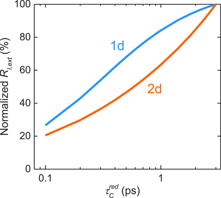
Until now, we made the simplifying assumption that Au contacts do not affect the e local cooling rate in SLG at (or under) the contacts, and assumed a fixed τC ∼ 3 ps34,75 everywhere. However, it is expected that Au ph and e may increase locally the SLG e cooling rate.97,98 The Au e–e and e–ph thermalization times were estimated in the 1–3 ps regime by theoretical105,106 and experimental107−111 works, with the smallest reported value ∼ 0.25 ps.110 Another source of increased cooling could be related to roughness in the metal contact. For the 1d case, on the other hand, increased cooling near the contact could originate by resonant dissipation from atomic defects along the SLG edge.99 To evaluate the effect of increased scattering, we assume a locally reduced cooling time τCred in SLG under the contact and up to a distance δ away from it (for the 1d contact τC involves only this δ). In the absence of experimental δ values, we assume, for simplicity and without loss of generality, δ = 25 nm as used in ref (98). τCred also lacks an experimental value, so it is used here as a free parameter. Simulations with τC reduced to 0.1 ps are shown in Figure 7 for the fully embedded TE mode case, with SLG EF = −0.07 eV, d = 20 nm, L = 30 μm, and w = 450 nm. RI,ext drops for smaller τCred, but at a faster rate for 2d compared to 1d contacts. This trend is reversed when τC approaches 0.1 ps. RI,ext reduces by 32% and 54% at τCred = 0.5 ps for the 1d and 2d cases, respectively. Thus, an increased e cooling rate at the contacts will impose a significant RI,ext reduction, more strongly for the 2d case, without however altering the main predictions of our work (see Methods).
Figure 7.
RI,ext as a function of τCred in SLG at/under the metal contact, normalized to RI,ext when τC = 3 ps.
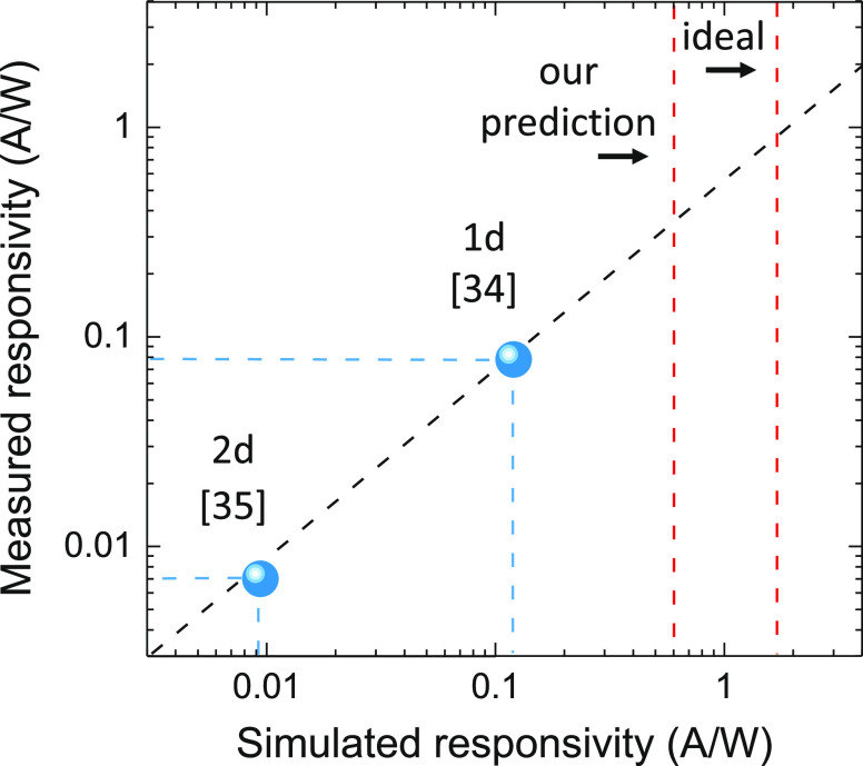
We next validate our results by comparing our model findings with the measurements of two similar devices, ref (35), where 2d contacts were used, and ref (34), where 1d ones were used (both in TE polarization). Simulations are done using the experimental device geometries of refs (34) and (35) detailed in Table 1. In the 2d case35 some missing information is assumed: in the experiment, there was no gate on SLG, so we assume p-doping EF = −0.14 eV.94,112 We assume μq = 2000 cm2/Vs as for ref (45), and a unit length contact resistance ρC = 1.2 kΩ μm.67 For the 1d case,34 we assume μq = 7000 cm2/Vs and ρC = 0.5 k Ωμm65 (in ref (34) μq = 1000 cm2/Vs was estimated, but with the effect of contact resistance integrated into the mobility), which, at the optimum |EF| ∼ 0.1 eV, yield RD ∼ 93 Ω, very close to the experimental value. For both contacts, we assume the same τC = 3 ps and τCred = 0.5 ps. Using the assumptions of Table 1, we reproduce the experimental resistance and RI,ext of refs (34) and (35). The final agreement between simulated and measured results confirms the validity of our model. A common τC = 0.5 ps assumption is adequate for both contact designs, confirming that there is faster cooling of SLG e at the metal contact. Small discrepancies between experiments and models can be due to a variety of reasons. Thus, rather than fitting τCred to coerce an exact agreement, we adopt τC = 0.5 ps as a reasonable assumption.
Table 1. Setup of Selected Experimental Devices (TE Polarization)34,35 and Comparison between Measurements and Simulations.
| contact type | 1d34 | 2d35 | ||
|---|---|---|---|---|
| device setup | device length L | 40 | 30 | μm |
| S–D distance W | 3 | 1.4 | μm | |
| contact distance d | 0.2 | 0.3 | μm | |
| WG width w | 0.52 | 0.4 | μm | |
| SLG-Si spacer thickness | 35 | 25 | nm | |
| electron cooling time τC | 3 | 3 | ps | |
| carrier mobility μq | 7000a | 2000a | cm2/Vs | |
| residual local charge n0* | 3b | 7b | (×1011) cm–2 | |
| graphene Fermi level EF | –0.11 | –0.14a | eV | |
| contact resistance ρC | 0.5a | 1.2a | kΩ μm | |
| measurements34,35 | graphene absorption αSLG | 40 | 35 | % |
| device resistance RD | 96 | 187 | Ω | |
| current responsivity RI,ext | 0.078 | 0.007 | A/W | |
| simulations | graphene absorption aSLG | 40 | 37 | % |
| device resistance RD | 93 | 187 | Ω | |
| current responsivity RI,ext | 0.12 | 0.0094 | A/W |
This confirms that RI,ext ∼ 0.6 A/W is possible, for L = 30 μm with the faster τCred = 0.5 ps at the contacts. In terms of external quantum efficiency (collected e–h pairs to incoming photons ratio30): EQE = RI,exthc/eλ ∼ 48%. By considering the simulated SLG absorption αSLG ∼ 50% (∼ 30% transmission and ∼ 20% scattering and parasitic contact absorption losses) in our best design, we get an internal quantum efficiency (collected e–h pairs to absorbed photons ratio30) IQE ∼ 100%. We note that high IQE (even >100%) are a result of carrier multiplication, i.e., the creation of multiple HCs per absorbed photon.46,76,77,81,82 HC multiplication and carrier heating is very efficient in SLG,77 and can be exploited for various applications.77
To put these numbers in perspective, we derive the ideal internal PTE performance (responsivity and quantum efficiency) to set a theoretical upper limit of an asymmetric contact architecture. We make two assumptions: (a) absorption occurs only in SLG (no scattering or metal absorption) and (b) absorption occurs in a δ-distribution width at the contact edge (maximized field confinement). Assuming that ΔTe exponentially decays in both x (along the source–drain) and y (along the WG) directions, its profile is given by:
| 1 |
where ΔTe0 is the peak Te rise,  is the cooling
length across the SLG channel,
and ψ is the decay length due to SLG absorption
along the WG length (used as a free parameter). κ and ce are the SLG heat conduction and capacity,
respectively. For a long device (L ≫ ψ), all light is absorbed, and we get the ideal internal
current responsivity (see Methods):
| 2 |
while for the smallest length (L → 0) we get the ideal voltage responsivity:
| 3 |
where g [Ω–1 m–1] is the device electrical conductance per
unit length, and  is a generalized
heat exchange coefficient.
For our SLG parameters (EF = −0.07
eV, τC = 3 ps, and μq = 10,000 cm2/Vs) for ideal (nonabsorbing) 1d contacts we find RI,int∞ ∼ 2.5 A/W (∼ 1.7 A/W if we include the 32% reduction
at τC = 0.5 ps). These correspond to ideal internal quantum efficiency
IQE∞ = 200% (136% for τCred = 0.5 ps). We find that our
proposed device is at ∼35% of the ideal performance (see Methods). If we include the metal absorption in
the infinite device (∼28%, extrapolated from the ∼20%
of the L = 30 μm device), we estimate RI,ext = 0.72 A/W and RI,int∞ = 1.22 A/W for the ideal case
of maximum field confinement (for τC = 0.5 ps and ρC =
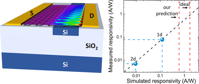
1 kΩ μm). Figure 8 puts all our findings into perspective, plotting the validation
studies and predicted performance (proposed and ideal) in one graph.
The excellent agreement between simulation and experiments (blue
points in Figure 8)
demonstrates the overall validity of our model.
Figure 8.
Simulated and measured RI,ext of the devices in refs (34) and (35) (blue points). The red lines mark the highest RI,ext prediction and the theoretical ideal internal RI,int∞ for integrated asymmetric PTE PDs, including the 32% reduction at τC = 0.5 ps.
We now consider other performance characteristics,
i.e., sensitivity
and speed. The sensitivity is quantified by the noise equivalent power
(NEP), defined as NEP = In/RI,ext, where In is the root-mean-square
noise current density per hertz of BW in A/Hz0.5.75 At the optimal operation point with RI,ext = 0.6 A/W (assuming the faster cooling
τCred =
0.5 ps at the contacts) and considering only thermal (Johnson) noise IJ (because of zero dark current)  (98) (see Methods), we estimate intrinsic NEP ∼ 22
pW/Hz0.5. An interesting comparison is with the sensitivity
of similar devices operated under a source–drain bias, VSD, in which case dark current enters the shot
noise. E.g., assuming VSD = 0.5 V31,45 and RD = 100 Ω, we find ID = 5 mA. Taking into consideration the shot
noise component, the total noise current spectral density becomes
  yielding, for RI,ext = 0.6 A/W, a NEP ∼70 pW/Hz0.5 at P = 2.5 mW power
consumption, more than triple the NEP of our unbiased device.
We estimated the RC time constant of the device using the cutoff frequency fc = {2πRD{[CG–1 + Cq(EF)−1]−1 + CSD}}−1, where CG is the capacitance due to local gates, Cq(EF) is the SLG quantum capacitance,114 and CSD is the parasitic device capacitance. We assume CSD = 20 fF as estimated in ref (35) for a similar device configuration. The gate capacitance is CG = εε0A/t, where ε0 = 8.85 × 10⁻¹² F/m is the vacuum permittivity, ε = 3.5 is the hBN static dielectric constant,115t = 10 nm is the hBN thickness between SLG and substrate, and A is the gated area. Cq(EF) = e2v(EF)A, where v(EF) is the SLG density of states at energy EF (see Methods). For the fully gated device (both WG and side) A = 30 × 1.1 μm2, while for a WG gate only, A = 30 × 0.35 μm2 (assuming the optimal TE configuration at L = 30 μm). For RD = 100 Ω and EF = −0.07 eV, the fully gated and WG-gated configurations yield cutoff frequencies fc ∼ 15 GHz and ∼ 34 GHz, respectively. If no gate is used, then fc can reach up to ∼ 80 GHz. We note that SLG τC ∼2–4 ps,46,82−89 and metal HC transfer/injection and cooling times of sub-ps116 and ps,108,117 result in a PTE-GPD intrinsic speed limit ∼1/τC ∼ 250–500 GHz, much larger than the estimated RC device characteristic frequency (<100 GHz), making the latter a good estimate for the expected BW.35
Conclusions
Given the absence of band gap in SLG, an unbiased operation is preferred for GPDs to avoid large dark currents, shot noise, power consumption, and unwanted joule heating. Placing the metal contacts asymmetrically with respect to WGs promotes plasmonic-assisted light absorption in the SLG channel and allows for unbiased photodetection. Comprehensive optical-thermal-electrical modeling shows that, by tuning the SLG EF and device architecture, high responsivity (RI,ext ∼ 0.6 A/W), sensitivity (NEP ∼ 22 pW/Hz0.5), and speed (f ∼ 80 GHz) can be achieved for integrated photonics. This architecture can be further enhanced with local gates, yielding independent control over device resistance and responsivity, towards integrated balanced photodetection. Comparison with refs (34) and (35) validates our model assumptions and predictions. Together with the derived analytical expression for the ideal performance, this gives a perspective and outlook for integrated GPDs. E.g., in the ideal responsivity we assumed a fixed cooling time (τC = 3 ps), carrier mobility (μq = 10,000 cm2/Vs), and contact resistance (ρC = 1 kΩ μm). Improving them will also increase responsivity (see Methods). Target areas of focus for improving performance should then be (i) increased SLG mobility (increased RI,ext and f), (ii) longer cooling time (increased RI,ext), and (iii) lower contact resistance (increased RI,ext and f). Given our design’s losses in scattering, transmission, and parasitic contact absorption, the focus should also be on (iv) improved plasmonic and/or metamaterial contact structures (less absorption losses). These pave the way toward RI,ext > 1 A/W, NEP <10 pW/Hz0.5, and f > 100 GHz in an unbiased integrated GPD.
Methods
Optical Modeling
Optical calculations are performed with the Finite-difference time-domain method (FDTD, Lumerical118). The computational cell dimensions are 4 × (L + 4) × 5 μm3, with perfectly matched layer (PML) conditions in all directions and with a 5 nm grid. The light source is the fundamental TE or TM optical mode of the Si WG at λ = 1550 nm. The dimensions of the device layers are given in Figure 1 and Table 1. The Au dielectric function is fitted with a Lumerical model.119 hBN is anisotropic120 with different permittivity in the in-plane (⊥) and out-of-plane (∥) directions. At λ = 1550 nm, its refractive index is120n⊥ = 2.187 and n∥ = 1.715. For SiO2 and Si, we use nSi = 3.4757121 and nSiO2 = 1.444.121 SLG is implemented as a 2d surface, with optical response modeled by the Kubo conductance122 σ = σintra + σinter:
| 4 |
| 5 |
where Ω = ω + iτopt–1, τopt is the scattering time, f(ε; μ, Te) = [e(ε–μ)/kBTe + 1]−1 is the Fermi–Dirac distribution, and ∂ε ≡ ∂/∂ε. τopt is related to EF and μq as τopt = μq|EF|/evF2,15 where vF = 106 ms–1 is the SLG Fermi velocity. For μq = 10,000 cm2/Vs and |EF| = 0.2 eV, we get τopt = 200 fs, used in eq 5.
Thermoelectric Modeling
We assume the quasi-cw case and solve the heat dissipation equation:74
| 6 |
where κ is the electronic thermal conductivity, Π = sTe is the Peltier coefficient, jq = −σs∇Te is the local thermoelectric current, σ is the electrical conductivity, ce is the electronic heat capacity, ΔT = Te – Tl, αden is the absorption density, and Pin is the incoming power. Note that in eq 6, −∇Π· jq = jq· (σ–1jq) – Tejq· ∇s, where the first term on the right is the Joule heating123 and the second term includes both Peltier124 (∇s at junction) and Thomson125 (∇s in thermal gradient) effects. Due to the large SLG lattice heat capacity (compared to the electronic one),90 we assume constant Tl = 300 K. The SLG parameters μ, σ, s, ce, κ, and αden are functions of EF and Te and are explicitly considered as such. The self-consistent solution of eq 6 provides the Te distribution, from which the thermoelectric voltage is obtained:
| 7 |
The photocurrent is then IPTE = VPTE/RD, where RD = RG + 2RC with  the SLG channel resistance and RC = ρC/L is
the contact resistance, with ρC being the unit length
contact resistance in units of Ω μm. Dividing by the input
power, we get the external responsivities RV,ext = VPTE/Pin and RI,ext = IPTE/Pin.
Zero bias PDs are
limited by the Johnson noise,98,126,127 when operating in frequencies
above the corner frequency f0 (defined
as the frequency where the flicker (1/f) noise is
equal to thermal or shot noise, typically ≤100 kHz for SLG
devices128), assuming that they are perfectly
shielded to minimize external noise and that have been impedance matched
to minimize the amplifier noise. Also, possible contributions from
generation–recombination noise, which occurs within the e–e
scattering time scale (<50 fs46,76,77), have a small effect on SLG’s local thermal
equilibrium which gives rise to the PTE response and are not considered
here. Thus the noise current (root-mean-square noise current density
per Hz of BW in A/Hz0.5) is  ,98 where kB is the
Boltzmann constant and T is the operation temperature
(300 K), and the intrinsic NEP = In/RI,ext in units
of W/Hz0.5. We note that a linear photoresponse as a function
of power is expected because the GPD operates in the weak heating
regime (ΔT ≪ Tambient), where
the electronic heat capacity can be considered constant.34,37,76,98
At finite Te we obtain the chemical
potential from the solution of103 ∫0∞v(ε)[f(ε; μ, Te) – f(ε; −μ, Te)]dε = EF2/πℏ2vF2, where v(ε) = 2|ε|/πℏ2vF2 is the SLG density
of states at energy ε. The other SLG electrical and thermal
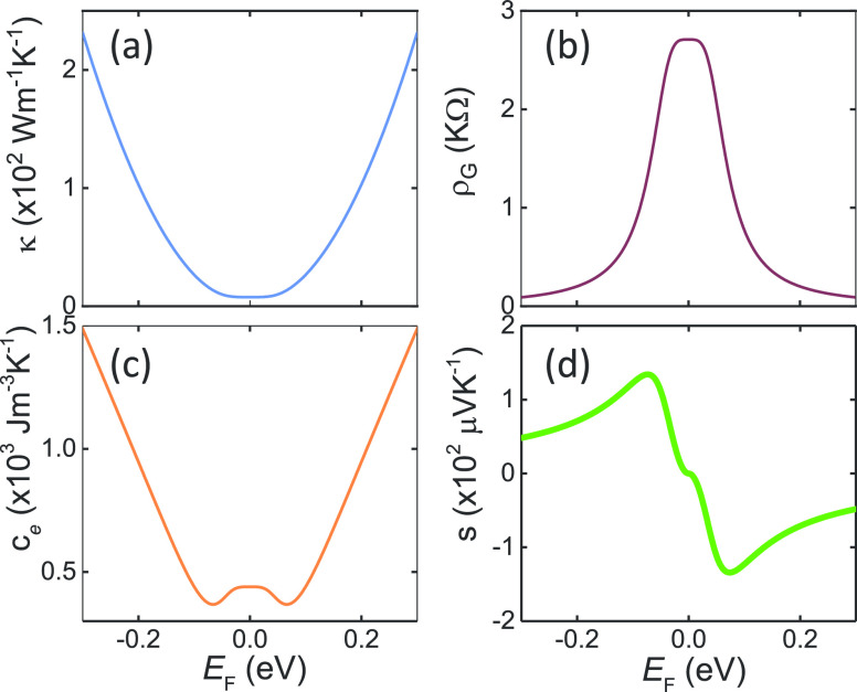
parameters in Figure 9 are calculated as follows: electrical conductivity σ(μ, Te) =  , where σ(ε)
= q[μqn(ε)
+ μ̅n*(ε)], with μq = μe/(μh) for ε > 0/(ε
< 0) and μ̅
= (μe + μh)/2. The effective residual
local charge fluctuation at energy ε is n*(ε)
=
  , where n(ε) = ε2/πℏ2vF2 is the SLG charge density
at energy ε and n0 is the residual local charge fluctuation
at the charge neutrality
point.129,130 From the Mott formula,131
 . The electronic heat capacity103
 , while thermal conductivity by the Wiedemann–Franz
law132 κ(μ, Te) = L0σ(μ, Te)Te, where L0 = 2.44 × 10⁻⁸ W Ω
K–2 is the Lorenz number.
Figure 9.
(a) Thermal conductivity, (b) specific resistivity, (c) thermal capacity, and (d) s as a function of SLG EF for e/h mobility μq = 10,000 cm2/Vs, residual local charge fluctuation n0* = 1011 cm–2, and operation temperature 300 K.
Model Assumptions
The thermoelectric
calculations assume
SLG with μq = 10,000 cm2/Vs75 for both e/h, residual local charge fluctuation n0* = 1011 cm–275 and τC = 3 ps.34,75 We use a typical
value of unit length contact resistance ρC = 1 kΩ
μm,65,67,75 which for
the 30 μm long device results in 2RC = 66.7 Ω. EF of the SLG channel
varies from −0.21 to 0.21 eV. The EF pinning under the metal contacts is fixed at – 0.15 eV.93 We introduce a narrow region extending 40 nm34,73,98 from the contact edge into the
SLG channel, within which the SLG EF linearly
scales back to the assumed channel EF.
For the double-gating architecture, the extension of the transition
region in the contact close to the WG is bound by d. Almost identical results are obtained by assuming full electrostatic
simulations, Figure 10. EF can be tuned by VG as EF =  where εhBN = 3.5115 is the hBN spacer relative dielectric
constant,
and thBN = 10 nm is its thickness. The
breakdown electric field for hBN is ∼2 MV/cm for polycrystalline115 and ∼8 MV/cm for single crystal.133 In our case, the VG = 1.67 V required to dope SLG up to |EF| = 0.21 eV (the upper limit of our simulations) will produce an
electric field ∼1.67 MV/cm, well below breakdown.
Figure 10.
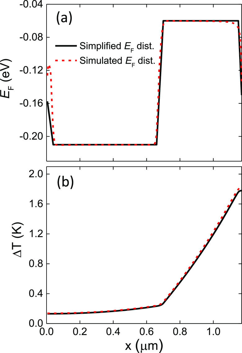
(a) EF spatial distribution across the SLG channel for the double-gating with “WG” EF = −0.06 eV and “side” EF = −0.21 eV. (b) Te increase distribution. The black solid lines correspond to results from the simplified EF spatial distribution presented in the main text, while the red dot lines are the results using the EF spatial distribution obtained by explicit electrostatic simulations.
Voltage Responsivity
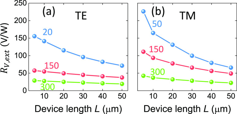
We adopt the 1d contact configuration, EF = −0.06 eV, and perform a series of optimization simulation runs, Figure 11, for both TE and TM polarizations to investigate the effect of device length on RV,ext. The trends are very similar, with a monotonic RV,ext increase for shorter devices. This is due to the higher absorption density in the first μms of the device.
Figure 11.
RV,ext (V/W) for SLG with EF = −0.06 eV at a 1d contact configuration, as a function of L (at fully embedded Si WG configuration and w = 450 nm). The numbers on the curves indicate different d. Panel (a) is for the TE, and panel (b) is for the TM mode.
Ideal PTE Responsivity and Quantum Efficiency
To estimate the ideal PTE internal responsivity and quantum efficiency, we assume that absorption occurs only in SLG and close to one of the contacts (e.g., at x = 0) with a fixed τC. At steady state, for x ≠ 0:
| 8 |
or
| 9 |
where  is the cooling length.
Assuming a decay
length ψ due to absorption along the WG length L, the Te profile can be written
as:
| 10 |
where ΔTe0 is the peak Te rise, and the variables x (y) run perpendicular (along) the WG. ψ is used as a free parameter. The power lost to phonons in steady state is ceτC–1ΔTe(x,y). By integration, we find the total power Pin:
| 11 |
The PTE voltage is found by integration over L (in the x direction we assume W is much larger than ξ):
| 12 |
The voltage responsivity is then:
| 13 |
where the term in the parenthesis accounts for light lost, that is, not absorbed, when L is comparable or smaller than ψ. By expanding ξ we find:
| 14 |
where  is a generalized
heat exchange coefficient
in W/mK. The max is at L → 0, where the absorbed
power density, thus Te, is the highest:
| 15 |
To find RI, we need the resistance as the sum of the SLG channel and contact contributions RD = RG + 2RC=(ρG′+2ρC)/L, with ρG = ρGW, ρG is the graphene specific resistivity, and ρC the contact resistance [Ω m]. Setting the device conductance per unit length g = (ρG′ + 2ρC)−1 [Ω–1 m–1] then:
| 16 |
RI increases as we increase the device length (voltage drops but resistance drops too). For long devices (i.e., all light is absorbed in the SLG channel) we get the ideal internal responsivity:
| 17 |
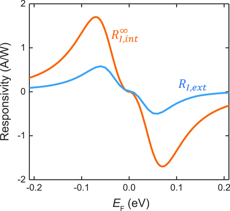
A comparison between RI,int∞ and RI,ext of our proposed design is shown in Figure 12. The ideal internal quantum efficiency is:30
| 18 |
Figure 12.
RI,int∞ and RI,ext for the double-gating architecture as a function of SLG channel EF and SLG “WG” EF, respectively (in the latter case, the “side” EF is set at EF = −0.2 eV). In both cases, we include the 32% reduction at τCred = 0.5 ps.
Effect of Mobility, Cooling Time, and Contact Resistance on Device Performance
We adopt the 1d contact configuration
and perform simulation runs for the optimum TE configuration of Figure 4 to investigate the
effect of μq, ρC, τC, and τCred on device performance. μq covers 5000–50,000
cm2/Vs, assuming a linear relation between 1/n0 and μq, according to ref (113). For τC, we use 1.5, 3, 5.5 ps, where
the last value was measured in WSe2-encapsulated SLG (WSe2/SLG/WSe2 stack with 124 nm total thickness, μq ≥ 10,000 cm2/Vs).89 As shown in Figure 13a, for zero contact resistance, higher μq and lower n0* result in monotonic increase of RI,ext. s saturates with improved SLG
quality (i.e., for μq ≥ 10,000 cm2/Vs, n0 ≤ 0.2 × 1012 cm–2)113,134 as the energy scale of n0* becomes
comparable to kBT,134Figure 13b. These RI,ext results
for ρC = 0 (channel limited) are consistent with eq 7, where g = (ρG)−1 ∝ μq and  , thus
  . When a finite ρC is introduced,
the trend changes, and the peak RI,ext is observed for lower μq as ρC increases. In the limit where the total device resistance is dominated
by the contact resistance g ∼ 1/2ρC (contact limited), the dominant contribution comes from the
increased thermal conductivity. Thus
  , i.e., reduced for increasing
μq.
Figure 13.
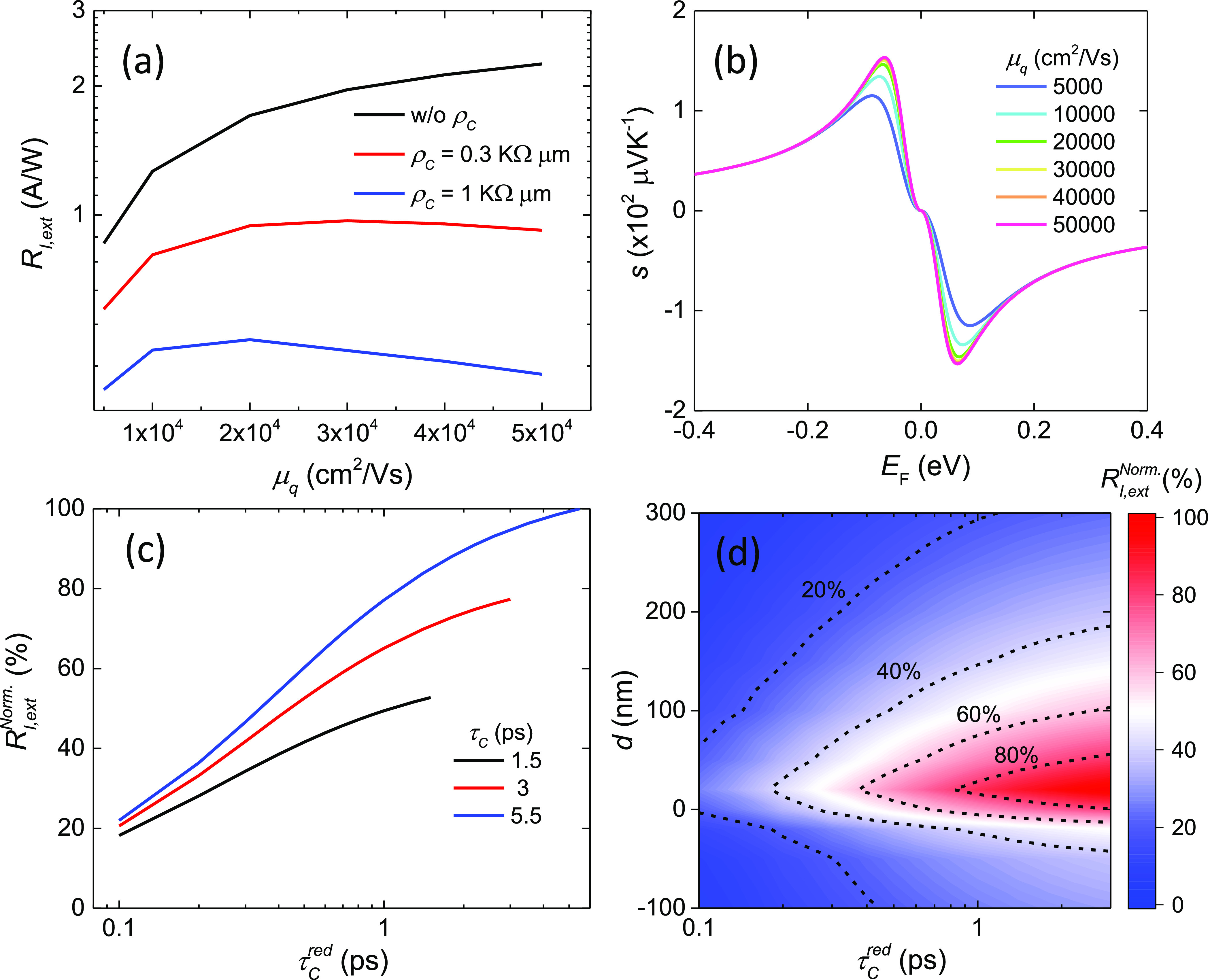
(a) RI,ext as a function of μq for three ρC for the optimal TE configuration of Figure 4 with τC = 3 ps and τCred = 0.5 ps. (b) s as a function of EF and μq. A linear relation between 1/n0 and μq is assumed as for ref (113). (c) RI,ext for EF = −0.07 eV, as a function of τC and τCred with ρC = 1 kΩ μm and μq = 10,000 cm2/Vs. All RI,ext are normalized to RI,ext when τC = τC = 5.5 ps. (d) RI,ext for EF = −0.07 eV as a function of τC and d. All RI,ext normalized to that for τCred = τC = 3 ps and d = 20 nm. All calculations for the TE mode, L = 30 μm, w = 450 nm, 1d contact, and fully embedded Si WG.
An increased cooling time improves RI,ext. As shown in Figure 13c, for τCred = τC, 90% and 30% increase in RI,ext is achieved for τC = 5.5 ps compared
to 1.5 and 3 ps, respectively, consistent with what is expected from
our analytical theory  . When we introduce faster cooling
at/under
the metal contact (τC < τC), the performance
differences diminish and converge to a common value. The faster cooling
at/under the metal contacts does not alter the optimum device configuration.
As shown in Figure 13d, the optimal d is unaffected by τCred.
Trade-off between Field Enhancement and Plasmonic Losses
As shown in Figures 2 and 14, the plasmonic excitation in the metal contacts results (as we reduce d) in field redistribution, enhanced field confinement, and increase of the SLG absorption density near the metal contact.
Figure 14.
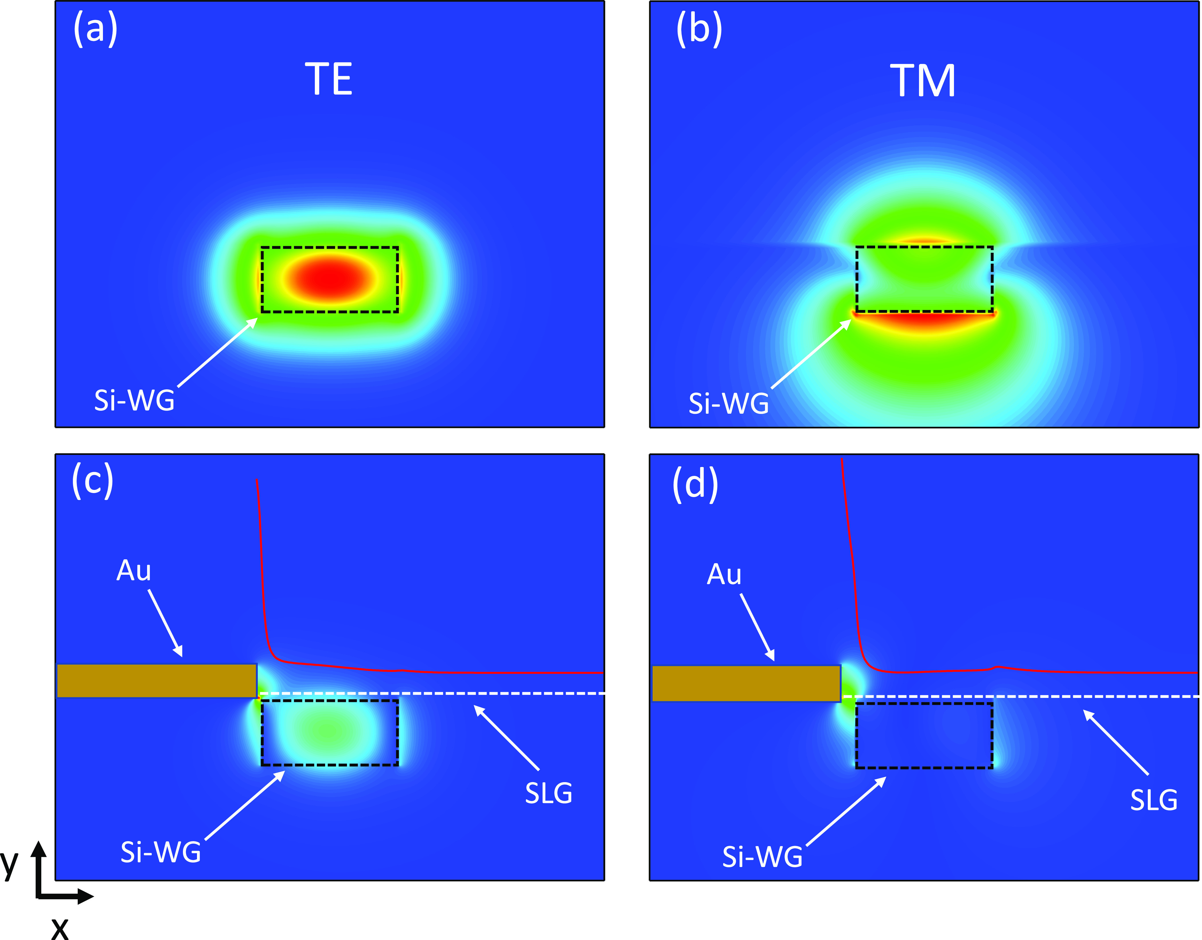
Si WG (w = 450 nm) optical mode field intensity profile for (a) TE and (b) TM polarization. |Ex| field component of the hybrid optical-plasmonic mode for (c) TE (d = 20 nm) and (d) TM (d = 50 nm). The SLG absorption profile is shown as a red line in (c,d). Calculations are for 1d contact and fully embedded Si WG.
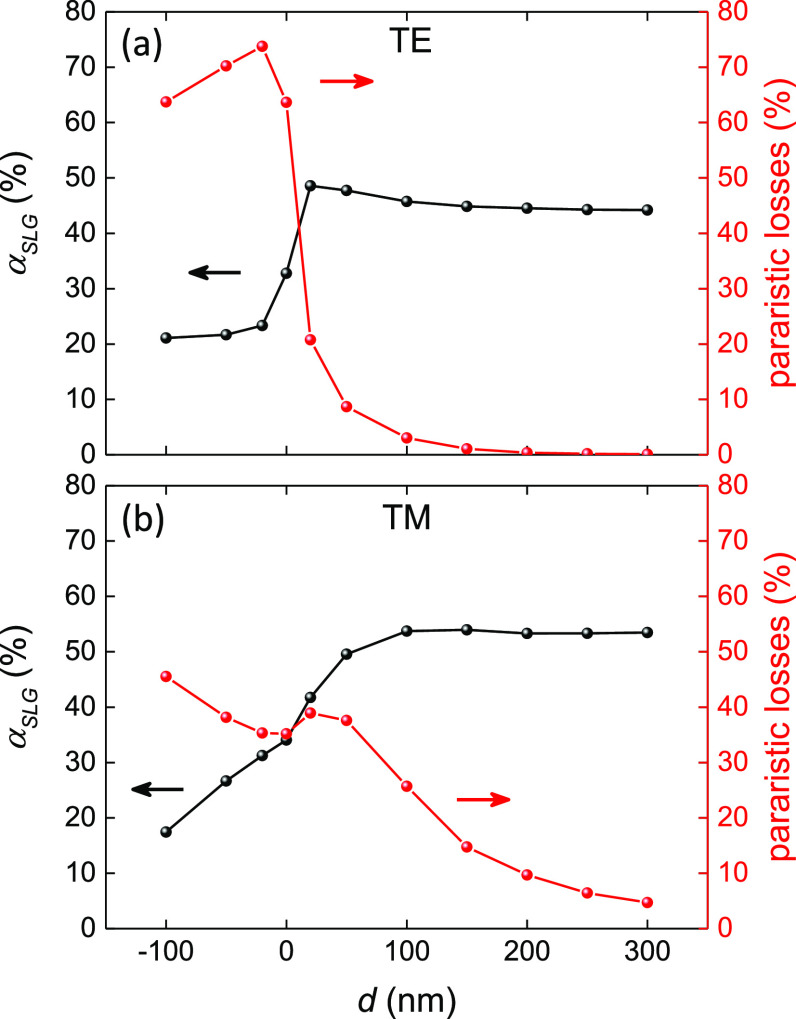
This increased absorption density is translated in larger Te and RI,ext with optimum d = 20 nm for TE and 50 nm for TM. To understand this behavior, we plot in Figure 15 the SLG absorption and the parasitic losses (metal absorption and scattering) as a function of d for both TE and TM modes. As d decreases to its optimal value, the gain from the increased plasmonic field confinement of the hybridized optical-SPP mode dominates the parasitic losses, yielding an enhanced Te gradient and RI,ext. Below the optimal d, metal losses and scattering increase at the expense of SLG absorption, resulting in reduced RI,ext, Figure 4.
Figure 15.
(a) SLG absorption, αSLG, and parasitic losses (metal absorption and scattering) as a function of d for (a) TE and (b) TM modes. Calculations are for w = 450 nm, L = 30 μm, fully embedded Si WG, 1d contacts.
Effect of Metal HC Injection/Transfer on Device Performance
As d reduces and the absorption in the metal contact increases due to the excitation of SPP modes (see Figure 15), photoexcited HC in the metal can in principle inject91 into the SLG channel and affect the responsivity.92 To quantify this, we estimate an upper limit of the metal HC contribution to the photocurrent using the optimized device (TE polarization, d = 20 nm) where we find a metal absorption αM ∼ 20% (see Figure 15a). If we assume all metal HCs with velocity normal to the interface to be injected and contribute to the photocurrent (i.e., 1/4 of them), then the metal HC current contribution is RI,HC = αM × 0.25 × e/ℏω = 0.0625 A/W. This corresponds to ∼ 10% of the maximum calculated RI,ext = 0.6 A/W. Given this upper limit, we expect the metal plasmonic HC effects to be a small correction.
We acknowledge funding from the Graphene and Quantum Flagships, EU Grant Plasmoniac, ERC grant Hetero2D, EPSRC grants EP/L016087/1, EP/K01711X/1, EP/K017144/1, EP/N010345/1, and DSTL. For the purpose of open access, the authors applied a Creative Commons Attribution (CC BY) license to any Author Accepted Manuscript version arising from this submission.
The authors declare no competing financial interest.
References
- Helkey R.; Saleh A. A. M.; Buckwalter J.; Bowers J. E. High-Performance Photonic Integrated Circuits on Silicon. IEEE J. Sel. Top. Quantum Electron. 2019, 25, 1–15. 10.1109/jstqe.2019.2903775. [DOI] [Google Scholar]
- Fathololoumi S.; et al. 1.6 Tbps Silicon Photonics Integrated Circuit and 800 Gbps Photonic Engine for Switch Co-Packaging Demonstration. J. Lightwave Technol. 2021, 39, 1155–1161. 10.1109/jlt.2020.3039218. [DOI] [Google Scholar]
- Pitris S.; Mitsolidou C.; Moralis-Pegios M.; Fotiadis K.; Ban Y.; De Heyn P.; Van Campenhout J.; Lambrecht J.; Ramon H.; Yin X.; Bauwelinck J.; Pleros N.; Alexoudi T. 400 Gb/s Silicon Photonic Transmitter and Routing WDM Technologies for Glueless 8-Socket Chip-to-Chip Interconnects. J. Lightwave Technol. 2020, 38, 3366–3375. 10.1109/jlt.2020.2977369. [DOI] [Google Scholar]
- Minzioni P.; et al. Roadmap on all-optical processing. J. Opt. 2019, 21, 063001. 10.1088/2040-8986/ab0e66. [DOI] [Google Scholar]
- Alexoudi T.; Kanellos G. T.; Pleros N. Optical RAM and integrated optical memories: a survey. Light: Sci. Appl. 2020, 9, 91. 10.1038/s41377-020-0325-9. [DOI] [PMC free article] [PubMed] [Google Scholar]
- Totović A. R.; Dabos G.; Passalis N.; Tefas A.; Pleros N. Femtojoule per MAC Neuromorphic Photonics: An Energy and Technology Roadmap. IEEE J. Sel. Top. Quantum Electron. 2020, 26, 1–15. 10.1109/jstqe.2020.2975579. [DOI] [Google Scholar]
- Shen Y.; Harris N. C.; Skirlo S.; Prabhu M.; Baehr-Jones T.; Hochberg M.; Sun X.; Zhao S.; Larochelle H.; Englund D.; Soljačić M. Deep learning with coherent nanophotonic circuits. Nat. Photonics 2017, 11, 441–446. 10.1038/nphoton.2017.93. [DOI] [Google Scholar]
- Shastri B. J.; Tait A. N.; Ferreira de Lima T.; Pernice W. H. P.; Bhaskaran H.; Wright C. D.; Prucnal P. R. Photonics for artificial intelligence and neuromorphic computing. Nat. Photonics 2021, 15, 102–114. 10.1038/s41566-020-00754-y. [DOI] [Google Scholar]
- Patrizio A.Ethernet Consortium Releases 800GbE Spec. https://www.networkworld.com/article/3538529/ethernet-consortium-releases-800gbespec.html (accessed Jan 12, 2021).
- Akinwande D.; Huyghebaert C.; Wang C.-H.; Serna M. I.; Goossens S.; Li L.-J.; Wong H.-S. P.; Koppens F. H. L. Graphene and two-dimensional materials for silicon technology. Nature 2019, 573, 507–518. 10.1038/s41586-019-1573-9. [DOI] [PubMed] [Google Scholar]
- Salamin Y.; Ma P.; Baeuerle B.; Emboras A.; Fedoryshyn Y.; Heni W.; Cheng B.; Josten A.; Leuthold J. 100 GHz Plasmonic Photodetector. ACS Photonics 2018, 5, 3291–3297. 10.1021/acsphotonics.8b00525. [DOI] [Google Scholar]
- Thomson D.; et al. Roadmap on silicon photonics. J. Opt. 2016, 18, 073003. 10.1088/2040-8978/18/7/073003. [DOI] [Google Scholar]
- Vivien L.; Osmond J.; Fédéli J.-M.; Marris-Morini D.; Crozat P.; Damlencourt J.-F.; Cassan E.; Lecunff Y.; Laval S. 42 GHz pin Germanium photodetector integrated in a silicon-on-insulator waveguide. Opt. Express 2009, 17, 6252–6257. 10.1364/oe.17.006252. [DOI] [PubMed] [Google Scholar]
- Stojanović V.; Ram R. J.; Popović M.; Lin S.; Moazeni S.; Wade M.; Sun C.; Alloatti L.; Atabaki A.; Pavanello F.; Mehta N.; Bhargava P. Monolithic silicon-photonic platforms in state-of-the-art CMOS SOI processes [Invited]. Opt. Express 2018, 26, 13106–13121. 10.1364/OE.26.013106. [DOI] [PubMed] [Google Scholar]
- Romagnoli M.; Sorianello V.; Midrio M.; Koppens F. H. L.; Huyghebaert C.; Neumaier D.; Galli P.; Templ W.; D’Errico A.; Ferrari A. C. Graphene-based integrated photonics for next-generation datacom and telecom. Nat. Rev. Mater. 2018, 3, 392–414. 10.1038/s41578-018-0040-9. [DOI] [Google Scholar]
- Hobbs P. C. D. Ultrasensitive laser measurements without tears. Appl. Opt. 1997, 36, 903–920. 10.1364/ao.36.000903. [DOI] [PubMed] [Google Scholar]
- Runge P.; Zhou G.; Beckerwerth T.; Ganzer F.; Keyvaninia S.; Seifert S.; Ebert W.; Mutschall S.; Seeger A.; Schell M. Waveguide Integrated Balanced Photodetectors for Coherent Receivers. IEEE J. Sel. Top. Quantum Electron. 2018, 24, 1–7. 10.1109/jstqe.2017.2723844. [DOI] [Google Scholar]
- Hai M. S.; Sakib M. N.; Liboiron-Ladouceur O. A 16 GHz silicon-based monolithic balanced photodetector with on-chip capacitors for 25 Gbaud front-end receivers. Opt. Express 2013, 21, 32680–32689. 10.1364/oe.21.032680. [DOI] [PubMed] [Google Scholar]
- Painchaud Y.; Poulin M.; Morin M.; Têtu M. Performance of balanced detection in a coherent receiver. Opt. Express 2009, 17, 3659–3672. 10.1364/oe.17.003659. [DOI] [PubMed] [Google Scholar]
- Wang J.; Lee S. Ge-photodetectors for Si-based optoelectronic integration. Sensors 2011, 11, 696–718. 10.3390/s110100696. [DOI] [PMC free article] [PubMed] [Google Scholar]
- Michel J.; Liu J.; Kimerling L. C. High-performance Ge-on-Si photodetectors. Nat. Photonics 2010, 4, 527–534. 10.1038/nphoton.2010.157. [DOI] [Google Scholar]
- Liang D.; Roelkens G.; Baets R.; Bowers J. Hybrid Integrated Platforms for Silicon Photonics. Materials 2010, 3, 1782–1802. 10.3390/ma3031782. [DOI] [Google Scholar]
- Beling A.; Campbell J. C. InP-Based High-Speed Photodetectors. J. Lightwave Technol. 2009, 27, 343–355. 10.1109/jlt.2008.2008399. [DOI] [Google Scholar]
- Chrostowski L.; Hochberg M.. Silicon Photonics Design: From Devices to Systems; Cambridge University Press, 2015. [Google Scholar]
- Ye H.; Yu J. Germanium epitaxy on silicon. Sci. Technol. Adv. Mater. 2014, 15, 024601. 10.1088/1468-6996/15/2/024601. [DOI] [PMC free article] [PubMed] [Google Scholar]
- Novack A.; Gould M.; Yang Y.; Xuan Z.; Streshinsky M.; Liu Y.; Capellini G.; Lim A. E.-J.; Lo G.-Q.; Baehr-Jones T.; Hochberg M. Germanium photodetector with 60 GHz bandwidth using inductive gain peaking. Opt. Express 2013, 21, 28387–28393. 10.1364/oe.21.028387. [DOI] [PubMed] [Google Scholar]
- Absil P. P.; Verheyen P.; De Heyn P.; Pantouvaki M.; Lepage G.; De Coster J.; Van Campenhout J. Silicon photonics integrated circuits: a manufacturing platform for high density, low power optical I/O’s. Opt. Express 2015, 23, 9369–9378. 10.1364/oe.23.009369. [DOI] [PubMed] [Google Scholar]
- Ferrari A. C.; et al. Science and technology roadmap for graphene, related two-dimensional crystals, and hybrid systems. Nanoscale 2015, 7, 4598–4810. 10.1039/c4nr01600a. [DOI] [PubMed] [Google Scholar]
- Bonaccorso F.; Sun Z.; Hasan T.; Ferrari A. C. Graphene photonics and optoelectronics. Nat. Photonics 2010, 4, 611–622. 10.1038/nphoton.2010.186. [DOI] [Google Scholar]
- Koppens F. H. L.; Mueller T.; Avouris P.; Ferrari A. C.; Vitiello M. S.; Polini M. Photodetectors based on graphene, other two-dimensional materials and hybrid systems. Nat. Nanotechnol. 2014, 9, 780–793. 10.1038/nnano.2014.215. [DOI] [PubMed] [Google Scholar]
- Ma P.; Salamin Y.; Baeuerle B.; Josten A.; Heni W.; Emboras A.; Leuthold J. Plasmonically Enhanced Graphene Photodetector Featuring 100 Gbit/s Data Reception, High Responsivity, and Compact Size. ACS Photonics 2019, 6, 154–161. 10.1021/acsphotonics.8b01234. [DOI] [Google Scholar]
- Gao Y.; Zhou G.; Zhao N.; Tsang H. K.; Shu C. High-performance chemical vapor deposited graphene-on-silicon nitride waveguide photodetectors. Opt. Lett. 2018, 43, 1399–1402. 10.1364/ol.43.001399. [DOI] [PubMed] [Google Scholar]
- Gan X.; Shiue R.-J.; Gao Y.; Meric I.; Heinz T. F.; Shepard K.; Hone J.; Assefa S.; Englund D. Chip-integrated ultrafast graphene photodetector with high responsivity. Nat. Photonics 2013, 7, 883–887. 10.1038/nphoton.2013.253. [DOI] [Google Scholar]
- Shiue R.-J.; Gao Y.; Wang Y.; Peng C.; Robertson A. D.; Efetov D. K.; Assefa S.; Koppens F. H. L.; Hone J.; Englund D. High-Responsivity Graphene-Boron Nitride Photodetector and Autocorrelator in a Silicon Photonic Integrated Circuit. Nano Lett. 2015, 15, 7288–7293. 10.1021/acs.nanolett.5b02368. [DOI] [PubMed] [Google Scholar]
- Schall D.; Neumaier D.; Mohsin M.; Chmielak B.; Bolten J.; Porschatis C.; Prinzen A.; Matheisen C.; Kuebart W.; Junginger B.; Templ W.; Giesecke A. L.; Kurz H. 50 GBit/s Photodetectors Based on Wafer-Scale Graphene for Integrated Silicon Photonic Communication Systems. ACS Photonics 2014, 1, 781–784. 10.1021/ph5001605. [DOI] [Google Scholar]
- Schuler S.; Schall D.; Neumaier D.; Dobusch L.; Bethge O.; Schwarz B.; Krall M.; Mueller T. Controlled Generation of a p-n Junction in a Waveguide Integrated Graphene Photodetector. Nano Lett. 2016, 16, 7107–7112. 10.1021/acs.nanolett.6b03374. [DOI] [PubMed] [Google Scholar]
- Muench J. E.; et al. Waveguide-Integrated, Plasmonic Enhanced Graphene Photodetectors. Nano Lett. 2019, 19, 7632–7644. 10.1021/acs.nanolett.9b02238. [DOI] [PubMed] [Google Scholar]
- Mišeikis V.; et al. Ultrafast, Zero-Bias, Graphene Photodetectors with Polymeric Gate Dielectric on Passive Photonic Waveguides. ACS Nano 2020, 14, 11190–11204. 10.1021/acsnano.0c02738. [DOI] [PMC free article] [PubMed] [Google Scholar]
- Marconi S.; Giambra M. A.; Montanaro A.; Mišeikis V.; Soresi S.; Tirelli S.; Galli P.; Buchali F.; Templ W.; Coletti C.; Sorianello V.; Romagnoli M. Photo thermal effect graphene detector featuring 105 Gbit s–1 NRZ and 120 Gbit s–1 PAM4 direct detection. Nat. Commun. 2021, 12, 806. 10.1038/s41467-021-21137-z. [DOI] [PMC free article] [PubMed] [Google Scholar]
- Schuler S.; Schall D.; Neumaier D.; Schwarz B.; Watanabe K.; Taniguchi T.; Mueller T. Graphene Photodetector Integrated on a Photonic Crystal Defect Waveguide. ACS Photonics 2018, 5, 4758–4763. 10.1021/acsphotonics.8b01128. [DOI] [Google Scholar]
- Ding Y.; Cheng Z.; Zhu X.; Yvind K.; Dong J.; Galili M.; Hu H.; Mortensen N. A.; Xiao S.; Oxenløwe L. K. Ultra-compact integrated graphene plasmonic photodetector with bandwidth above 110 GHz. Nanophotonics 2020, 9, 317–325. 10.1515/nanoph-2019-0167. [DOI] [Google Scholar]
- Ma Z.; Kikunaga K.; Wang H.; Sun S.; Amin R.; Maiti R.; Tahersima M. H.; Dalir H.; Miscuglio M.; Sorger V. J. Compact Graphene Plasmonic Slot Photodetector on Silicon-on-Insulator with High Responsivity. ACS Photonics 2020, 7, 932–940. 10.1021/acsphotonics.9b01452. [DOI] [Google Scholar]
- Goykhman I.; Sassi U.; Desiatov B.; Mazurski N.; Milana S.; de Fazio D.; Eiden A.; Khurgin J.; Shappir J.; Levy U.; Ferrari A. C. On-Chip Integrated, Silicon-Graphene Plasmonic Schottky Photodetector with High Responsivity and Avalanche Photogain. Nano Lett. 2016, 16, 3005–3013. 10.1021/acs.nanolett.5b05216. [DOI] [PMC free article] [PubMed] [Google Scholar]
- Schuler S.; Muench J. E.; Ruocco A.; Balci O.; Thourhout D. v.; Sorianello V.; Romagnoli M.; Watanabe K.; Taniguchi T.; Goykhman I.; Ferrari A. C.; Mueller T. High-responsivity graphene photodetectors integrated on silicon microring resonators. Nat. Commun. 2021, 12, 3733. 10.1038/s41467-021-23436-x. [DOI] [PMC free article] [PubMed] [Google Scholar]
- Schall D.; Pallecchi E.; Ducournau G.; Avramovic V.; Otto M.; Neumaier D.. Record High Bandwidth Integrated Graphene Photodetectors for Communication beyond 180 Gb/s. 2018 Optical Fiber Communications Conference and Exposition; OFC, 2018; pp 1–3. [Google Scholar]
- Brida D.; Tomadin A.; Manzoni C.; Kim Y. J.; Lombardo A.; Milana S.; Nair R. R.; Novoselov K. S.; Ferrari A. C.; Cerullo G.; Polini M. Ultrafast collinear scattering and carrier multiplication in graphene. Nat. Commun. 2013, 4, 1987. 10.1038/ncomms2987. [DOI] [PubMed] [Google Scholar]
- Mayorov A. S.; Elias D. C.; Mucha-Kruczynski M.; Gorbachev R. V.; Tudorovskiy T.; Zhukov A.; Morozov S. V.; Katsnelson M. I.; Geim A. K.; Novoselov K. S. Interaction-Driven Spectrum Reconstruction in Bilayer Graphene. Science 2011, 333, 860–863. 10.1126/science.1208683. [DOI] [PubMed] [Google Scholar]
- Bolotin K. I.; Sikes K. J.; Jiang Z.; Klima M.; Fudenberg G.; Hone J.; Kim P.; Stormer H. L. Ultrahigh electron mobility in suspended graphene. Solid State Commun. 2008, 146, 351–355. 10.1016/j.ssc.2008.02.024. [DOI] [Google Scholar]
- Dorgan V. E.; Bae M.-H.; Pop E. Mobility and saturation velocity in graphene on SiO2. Appl. Phys. Lett. 2010, 97, 082112. 10.1063/1.3483130. [DOI] [Google Scholar]
- De Fazio D.; Purdie D. G.; Ott A. K.; Braeuninger-Weimer P.; Khodkov T.; Goossens S.; Taniguchi T.; Watanabe K.; Livreri P.; Koppens F. H. L.; Hofmann S.; Goykhman I.; Ferrari A. C.; Lombardo A. High-Mobility, Wet-Transferred Graphene Grown by Chemical Vapor Deposition. ACS Nano 2019, 13, 8926–8935. 10.1021/acsnano.9b02621. [DOI] [PubMed] [Google Scholar]
- Purdie D. G.; Pugno N. M.; Taniguchi T.; Watanabe K.; Ferrari A. C.; Lombardo A. Cleaning interfaces in layered materials heterostructures. Nat. Commun. 2018, 9, 5387. 10.1038/s41467-018-07558-3. [DOI] [PMC free article] [PubMed] [Google Scholar]
- Pospischil A.; Humer M.; Furchi M. M.; Bachmann D.; Guider R.; Fromherz T.; Mueller T. CMOS-compatible graphene photodetector covering all optical communication bands. Nat. Photonics 2013, 7, 892–896. 10.1038/nphoton.2013.240. [DOI] [Google Scholar]
- Giambra M. A.; Mišeikis V.; Pezzini S.; Marconi S.; Montanaro A.; Fabbri F.; Sorianello V.; Ferrari A. C.; Coletti C.; Romagnoli M. Wafer-Scale Integration of Graphene-Based Photonic Devices. ACS Nano 2021, 15, 3171–3187. 10.1021/acsnano.0c09758. [DOI] [PMC free article] [PubMed] [Google Scholar]
- Das A.; Pisana S.; Chakraborty B.; Piscanec S.; Saha S. K.; Waghmare U. V.; Novoselov K. S.; Krishnamurthy H. R.; Geim A. K.; Ferrari A. C.; Sood A. K. Monitoring dopants by Raman scattering in an electrochemically top-gated graphene transistor. Nat. Nanotechnol. 2008, 3, 210–215. 10.1038/nnano.2008.67. [DOI] [PubMed] [Google Scholar]
- Pisana S.; Lazzeri M.; Casiraghi C.; Novoselov K. S.; Geim A. K.; Ferrari A. C.; Mauri F. Breakdown of the adiabatic Born-Oppenheimer approximation in graphene. Nat. Mater. 2007, 6, 198–201. 10.1038/nmat1846. [DOI] [PubMed] [Google Scholar]
- Li Z. Q.; Henriksen E. A.; Jiang Z.; Hao Z.; Martin M. C.; Kim P.; Stormer H. L.; Basov D. N. Dirac charge dynamics in graphene by infrared spectroscopy. Nat. Phys. 2008, 4, 532–535. 10.1038/nphys989. [DOI] [Google Scholar]
- Wang F.; Zhang Y.; Tian C.; Girit C.; Zettl A.; Crommie M.; Shen Y. R. Gate-Variable Optical Transitions in Graphene. Science 2008, 320, 206–209. 10.1126/science.1152793. [DOI] [PubMed] [Google Scholar]
- Nair R. R.; Blake P.; Grigorenko A. N.; Novoselov K. S.; Booth T. J.; Stauber T.; Peres N. M. R.; Geim A. K. Fine Structure Constant Defines Visual Transparency of Graphene. Science 2008, 320, 1308. 10.1126/science.1156965. [DOI] [PubMed] [Google Scholar]
- Dawlaty J. M.; Shivaraman S.; Strait J.; George P.; Chandrashekhar M.; Rana F.; Spencer M. G.; Veksler D.; Chen Y. Measurement of the optical absorption spectra of epitaxial graphene from terahertz to visible. Appl. Phys. Lett. 2008, 93, 131905. 10.1063/1.2990753. [DOI] [Google Scholar]
- Freitag M.; Low T.; Xia F.; Avouris P. Photoconductivity of biased graphene. Nat. Photonics 2013, 7, 53–59. 10.1038/nphoton.2012.314. [DOI] [Google Scholar]
- Castro Neto A. H.; Guinea F.; Peres N. M. R.; Novoselov K. S.; Geim A. K. The electronic properties of graphene. Rev. Mod. Phys. 2009, 81, 109–162. 10.1103/revmodphys.81.109. [DOI] [Google Scholar]
- Gabor N. M.; Song J. C. W.; Ma Q.; Nair N. L.; Taychatanapat T.; Watanabe K.; Taniguchi T.; Levitov L. S.; Jarillo-Herrero P. Hot Carrier-Assisted Intrinsic Photoresponse in Graphene. Science 2011, 334, 648–652. 10.1126/science.1211384. [DOI] [PubMed] [Google Scholar]
- Echtermeyer T. J.; Milana S.; Sassi U.; Eiden A.; Wu M.; Lidorikis E.; Ferrari A. C. Surface Plasmon Polariton Graphene Photodetectors. Nano Lett. 2016, 16, 8–20. 10.1021/acs.nanolett.5b02051. [DOI] [PubMed] [Google Scholar]
- Dean C. R.; Young A. F.; Meric I.; Lee C.; Wang L.; Sorgenfrei S.; Watanabe K.; Taniguchi T.; Kim P.; Shepard K. L.; Hone J. Boron nitride substrates for high-quality graphene electronics. Nat. Nanotechnol. 2010, 5, 722–726. 10.1038/nnano.2010.172. [DOI] [PubMed] [Google Scholar]
- Wang L.; Meric I.; Huang P. Y.; Gao Q.; Gao Y.; Tran H.; Taniguchi T.; Watanabe K.; Campos L. M.; Muller D. A.; Guo J.; Kim P.; Hone J.; Shepard K. L.; Dean C. R. One-Dimensional Electrical Contact to a Two-Dimensional Material. Science 2013, 342, 614–617. 10.1126/science.1244358. [DOI] [PubMed] [Google Scholar]
- Giubileo F.; Di Bartolomeo A. The role of contact resistance in graphene field-effect devices. Prog. Surf. Sci. 2017, 92, 143–175. 10.1016/j.progsurf.2017.05.002. [DOI] [Google Scholar]
- Xia F.; Perebeinos V.; Lin Y.-m.; Wu Y.; Avouris P. The origins and limits of metal-graphene junction resistance. Nat. Nanotechnol. 2011, 6, 179–184. 10.1038/nnano.2011.6. [DOI] [PubMed] [Google Scholar]
- Park J.; Ahn Y. H.; Ruiz-Vargas C. Imaging of Photocurrent Generation and Collection in Single-Layer Graphene. Nano Lett. 2009, 9, 1742–1746. 10.1021/nl8029493. [DOI] [PubMed] [Google Scholar]
- Echtermeyer T. J.; Nene P. S.; Trushin M.; Gorbachev R. V.; Eiden A. L.; Milana S.; Sun Z.; Schliemann J.; Lidorikis E.; Novoselov K. S.; Ferrari A. C. Photothermoelectric and Photoelectric Contributions to Light Detection in Metal-Graphene-Metal Photodetectors. Nano Lett. 2014, 14, 3733–3742. 10.1021/nl5004762. [DOI] [PubMed] [Google Scholar]
- Lee E. J. H.; Balasubramanian K.; Weitz R. T.; Burghard M.; Kern K. Contact and edge effects in graphene devices. Nat. Nanotechnol. 2008, 3, 486–490. 10.1038/nnano.2008.172. [DOI] [PubMed] [Google Scholar]
- Mueller T.; Xia F.; Freitag M.; Tsang J.; Avouris P. Role of contacts in graphene transistors: A scanning photocurrent study. Phys. Rev. B 2009, 79, 245430. 10.1103/physrevb.79.245430. [DOI] [Google Scholar]
- Tielrooij K. J.; Massicotte M.; Piatkowski L.; Woessner A.; Ma Q.; Jarillo-Herrero P.; Hulst N. F. v.; Koppens F. H. L. Hot-carrier photocurrent effects at graphene-metal interfaces. J. Phys.: Condens. Matter 2015, 27, 164207. 10.1088/0953-8984/27/16/164207. [DOI] [PubMed] [Google Scholar]
- Mueller T.; Xia F.; Avouris P. Graphene photodetectors for high-speed optical communications. Nat. Photonics 2010, 4, 297–301. 10.1038/nphoton.2010.40. [DOI] [Google Scholar]
- Song J. C. W.; Rudner M. S.; Marcus C. M.; Levitov L. S. Hot Carrier Transport and Photocurrent Response in Graphene. Nano Lett. 2011, 11, 4688–4692. 10.1021/nl202318u. [DOI] [PubMed] [Google Scholar]
- Castilla S.; et al. Plasmonic antenna coupling to hyperbolic phonon-polaritons for sensitive and fast mid-infrared photodetection with graphene. Nat. Commun. 2020, 11, 4872. 10.1038/s41467-020-18544-z. [DOI] [PMC free article] [PubMed] [Google Scholar]
- Tielrooij K. J.; Piatkowski L.; Massicotte M.; Woessner A.; Ma Q.; Lee Y.; Myhro K. S.; Lau C. N.; Jarillo-Herrero P.; van Hulst N. F.; Koppens F. H. L. Generation of photovoltage in graphene on a femtosecond timescale through efficient carrier heating. Nat. Nanotechnol. 2015, 10, 437–443. 10.1038/nnano.2015.54. [DOI] [PubMed] [Google Scholar]
- Massicotte M.; Soavi G.; Principi A.; Tielrooij K.-J. Hot carriers in graphene - fundamentals and applications. Nanoscale 2021, 13, 8376–8411. 10.1039/d0nr09166a. [DOI] [PMC free article] [PubMed] [Google Scholar]
- Winzer T.; Knorr A.; Malic E. Carrier Multiplication in Graphene. Nano Lett. 2010, 10, 4839–4843. 10.1021/nl1024485. [DOI] [PubMed] [Google Scholar]
- Plötzing T.; Winzer T.; Malic E.; Neumaier D.; Knorr A.; Kurz H. Experimental Verification of Carrier Multiplication in Graphene. Nano Lett. 2014, 14, 5371–5375. 10.1021/nl502114w. [DOI] [PubMed] [Google Scholar]
- Song J. C. W.; Tielrooij K. J.; Koppens F. H. L.; Levitov L. S. Photoexcited carrier dynamics and impact-excitation cascade in graphene. Phys. Rev. B 2013, 87, 155429. 10.1103/physrevb.87.155429. [DOI] [Google Scholar]
- Tielrooij K. J.; Song J. C. W.; Jensen S. A.; Centeno A.; Pesquera A.; Zurutuza Elorza A.; Bonn M.; Levitov L. S.; Koppens F. H. L. Photoexcitation cascade and multiple hot-carrier generation in graphene. Nat. Phys. 2013, 9, 248–252. 10.1038/nphys2564. [DOI] [Google Scholar]
- Tomadin A.; Brida D.; Cerullo G.; Ferrari A. C.; Polini M. Nonequilibrium dynamics of photoexcited electrons in graphene: Collinear scattering, Auger processes, and the impact of screening. Phys. Rev. B 2013, 88, 035430. 10.1103/physrevb.88.035430. [DOI] [Google Scholar]
- Song J. C. W.; Levitov L. S. Energy flows in graphene: hot carrier dynamics and cooling. J. Phys.: Condens. Matter 2015, 27, 164201. 10.1088/0953-8984/27/16/164201. [DOI] [PubMed] [Google Scholar]
- Urich A.; Unterrainer K.; Mueller T. Intrinsic Response Time of Graphene Photodetectors. Nano Lett. 2011, 11, 2804–2808. 10.1021/nl2011388. [DOI] [PMC free article] [PubMed] [Google Scholar]
- Johannsen J. C.; Ulstrup S.; Cilento F.; Crepaldi A.; Zacchigna M.; Cacho C.; Turcu I. C.; Springate E.; Fromm F.; Raidel C.; Seyller T.; Parmigiani F.; Grioni M.; Hofmann P. Direct View of Hot Carrier Dynamics in Graphene. Phys. Rev. Lett. 2013, 111, 027403. 10.1103/PhysRevLett.111.027403. [DOI] [PubMed] [Google Scholar]
- Graham M. W.; Shi S.-F.; Ralph D. C.; Park J.; McEuen P. L. Photocurrent measurements of supercollision cooling in graphene. Nat. Phys. 2013, 9, 103–108. 10.1038/nphys2493. [DOI] [Google Scholar]
- Tielrooij K.-J.; et al. Out-of-plane heat transfer in van der Waals stacks through electron-hyperbolic phonon coupling. Nat. Nanotechnol. 2018, 13, 41–46. 10.1038/s41565-017-0008-8. [DOI] [PubMed] [Google Scholar]
- Lazzeri M.; Piscanec S.; Mauri F.; Ferrari A. C.; Robertson J. Electron Transport and Hot Phonons in Carbon Nanotubes. Phys. Rev. Lett. 2005, 95, 236802. 10.1103/physrevlett.95.236802. [DOI] [PubMed] [Google Scholar]
- Pogna E. A. A.; et al. Hot-Carrier Cooling in High-Quality Graphene Is Intrinsically Limited by Optical Phonons. ACS Nano 2021, 15, 11285–11295. 10.1021/acsnano.0c10864. [DOI] [PMC free article] [PubMed] [Google Scholar]
- Pop E.; Varshney V.; Roy A. K. Thermal properties of graphene: Fundamentals and applications. MRS Bull. 2012, 37, 1273–1281. 10.1557/mrs.2012.203. [DOI] [Google Scholar]
- Fang Z.; Wang Y.; Liu Z.; Schlather A.; Ajayan P. M.; Koppens F. H. L.; Nordlander P.; Halas N. J. Plasmon-Induced Doping of Graphene. ACS Nano 2012, 6, 10222–10228. 10.1021/nn304028b. [DOI] [PubMed] [Google Scholar]
- Fang Z.; Liu Z.; Wang Y.; Ajayan P. M.; Nordlander P.; Halas N. J. Graphene-Antenna Sandwich Photodetector. Nano Lett. 2012, 12, 3808–3813. 10.1021/nl301774e. [DOI] [PubMed] [Google Scholar]
- Giovannetti G.; Khomyakov P. A.; Brocks G.; Karpan V. M.; van den Brink J.; Kelly P. J. Doping Graphene with Metal Contacts. Phys. Rev. Lett. 2008, 101, 026803. 10.1103/PhysRevLett.101.026803. [DOI] [PubMed] [Google Scholar]
- Casiraghi C.; Pisana S.; Novoselov K. S.; Geim A. K.; Ferrari A. C. Raman fingerprint of charged impurities in graphene. Appl. Phys. Lett. 2007, 91, 233108. 10.1063/1.2818692. [DOI] [Google Scholar]
- Rhodes D.; Chae S. H.; Ribeiro-Palau R.; Hone J. Disorder in van der Waals heterostructures of 2D materials. Nat. Mater. 2019, 18, 541–549. 10.1038/s41563-019-0366-8. [DOI] [PubMed] [Google Scholar]
- Decker R.; Wang Y.; Brar V. W.; Regan W.; Tsai H.-Z.; Wu Q.; Gannett W.; Zettl A.; Crommie M. F. Local Electronic Properties of Graphene on a BN Substrate via Scanning Tunneling Microscopy. Nano Lett. 2011, 11, 2291–2295. 10.1021/nl2005115. [DOI] [PubMed] [Google Scholar]
- Sundaram R. S.; Steiner M.; Chiu H.-Y.; Engel M.; Bol A. A.; Krupke R.; Burghard M.; Kern K.; Avouris P. The Graphene-Gold Interface and Its Implications for Nanoelectronics. Nano Lett. 2011, 11, 3833–3837. 10.1021/nl201907u. [DOI] [PubMed] [Google Scholar]
- Castilla S.; Terrés B.; Autore M.; Viti L.; Li J.; Nikitin A. Y.; Vangelidis I.; Watanabe K.; Taniguchi T.; Lidorikis E.; Vitiello M. S.; Hillenbrand R.; Tielrooij K.-J.; Koppens F. H. L. Fast and Sensitive Terahertz Detection Using an Antenna-Integrated Graphene pn Junction. Nano Lett. 2019, 19, 2765–2773. 10.1021/acs.nanolett.8b04171. [DOI] [PubMed] [Google Scholar]
- Halbertal D.; Ben Shalom M.; Uri A.; Bagani K.; Meltzer A. Y.; Marcus I.; Myasoedov Y.; Birkbeck J.; Levitov L. S.; Geim A. K.; Zeldov E. Imaging resonant dissipation from individual atomic defects in graphene. Science 2017, 358, 1303–1306. 10.1126/science.aan0877. [DOI] [PubMed] [Google Scholar]
- AlAloul M.; Rasras M. Plasmon-enhanced graphene photodetector with CMOS-compatible titanium nitride. J. Opt. Soc. Am. B 2021, 38, 602–610. 10.1364/josab.416520. [DOI] [Google Scholar]
- Gosciniak J.; Rasras M.; Khurgin J. B. Ultrafast Plasmonic Graphene Photodetector Based on the Channel Photothermoelectric Effect. ACS Photonics 2020, 7, 488–498. 10.1021/acsphotonics.9b01585. [DOI] [Google Scholar]
- Enescu D.Green Energy Advances; Enescu D., Ed.; IntechOpen: Rijeka, 2019, Chapter 1. [Google Scholar]
- Soavi G.; et al. Broadband, electrically tunable third-harmonic generation in graphene. Nat. Nanotechnol. 2018, 13, 583–588. 10.1038/s41565-018-0145-8. [DOI] [PubMed] [Google Scholar]
- Cheng F.Thermoelectrics for Power Generation; Skipidarov S., Nikitin M., Eds.; IntechOpen: Rijeka, 2016, Chapter 19. [Google Scholar]
- Saavedra J. R. M.; Asenjo-Garcia A.; García de Abajo F. J. Hot-Electron Dynamics and Thermalization in Small Metallic Nanoparticles. ACS Photonics 2016, 3, 1637–1646. 10.1021/acsphotonics.6b00217. [DOI] [Google Scholar]
- Liu J. G.; Zhang H.; Link S.; Nordlander P. Relaxation of Plasmon-Induced Hot Carriers. ACS Photonics 2018, 5, 2584–2595. 10.1021/acsphotonics.7b00881. [DOI] [Google Scholar]
- Fann W. S.; Storz R.; Tom H. W. K.; Bokor J. Electron thermalization in gold. Phys. Rev. B 1992, 46, 13592–13595. 10.1103/physrevb.46.13592. [DOI] [PubMed] [Google Scholar]
- Sun C.-K.; Vallée F.; Acioli L. H.; Ippen E. P.; Fujimoto J. G. Femtosecond-tunable measurement of electron thermalization in gold. Phys. Rev. B 1994, 50, 15337–15348. 10.1103/physrevb.50.15337. [DOI] [PubMed] [Google Scholar]
- Link S.; El-Sayed M. A. Spectral Properties and Relaxation Dynamics of Surface Plasmon Electronic Oscillations in Gold and Silver Nanodots and Nanorods. J. Phys. Chem. B 1999, 103, 8410–8426. 10.1021/jp9917648. [DOI] [Google Scholar]
- Voisin C.; Christofilos D.; Loukakos P. A.; Del Fatti N.; Vallée F.; Lermé J.; Gaudry M.; Cottancin E.; Pellarin M.; Broyer M. Ultrafast electron-electron scattering and energy exchanges in noble-metal nanoparticles. Phys. Rev. B 2004, 69, 195416. 10.1103/physrevb.69.195416. [DOI] [Google Scholar]
- Dowgiallo A.-M.; Knappenberger K. L. Ultrafast electron-phonon coupling in hollow gold nanospheres. Phys. Chem. Chem. Phys. 2011, 13, 21585–21592. 10.1039/c1cp22743b. [DOI] [PubMed] [Google Scholar]
- Casiraghi C. Probing disorder and charged impurities in graphene by Raman spectroscopy. Phys. Status Solidi RRL 2009, 3, 175–177. 10.1002/pssr.200903135. [DOI] [Google Scholar]
- Couto N. J. G.; Costanzo D.; Engels S.; Ki D.-K.; Watanabe K.; Taniguchi T.; Stampfer C.; Guinea F.; Morpurgo A. F. Random Strain Fluctuations as Dominant Disorder Source for High-Quality On-Substrate Graphene Devices. Phys. Rev. X 2014, 4, 041019. 10.1103/physrevx.4.041019. [DOI] [Google Scholar]
- Fang T.; Konar A.; Xing H.; Jena D. Carrier statistics and quantum capacitance of graphene sheets and ribbons. Appl. Phys. Lett. 2007, 91, 092109. 10.1063/1.2776887. [DOI] [Google Scholar]
- Kim K. K.; Hsu A.; Jia X.; Kim S. M.; Shi Y.; Dresselhaus M.; Palacios T.; Kong J. Synthesis and Characterization of Hexagonal Boron Nitride Film as a Dielectric Layer for Graphene Devices. ACS Nano 2012, 6, 8583–8590. 10.1021/nn301675f. [DOI] [PubMed] [Google Scholar]
- Hoggard A.; Wang L.-Y.; Ma L.; Fang Y.; You G.; Olson J.; Liu Z.; Chang W.-S.; Ajayan P. M.; Link S. Using the Plasmon Linewidth To Calculate the Time and Efficiency of Electron Transfer between Gold Nanorods and Graphene. ACS Nano 2013, 7, 11209–11217. 10.1021/nn404985h. [DOI] [PMC free article] [PubMed] [Google Scholar]
- Brongersma M. L.; Halas N. J.; Nordlander P. Plasmon-induced hot carrier science and technology. Nat. Nanotechnol. 2015, 10, 25–34. 10.1038/nnano.2014.311. [DOI] [PubMed] [Google Scholar]
- Lumerical Inc. . https://www.lumerical.com/products/fdtd/ (accessed Feb 06, 2021).
- Johnson P. B.; Christy R. W. Optical Constants of the Noble Metals. Phys. Rev. B 1972, 6, 4370–4379. 10.1103/physrevb.6.4370. [DOI] [Google Scholar]
- Woessner A.; Lundeberg M. B.; Gao Y.; Principi A.; Alonso-González P.; Carrega M.; Watanabe K.; Taniguchi T.; Vignale G.; Polini M.; Hone J.; Hillenbrand R.; Koppens F. H. L. Highly confined low-loss plasmons in graphene-boron nitride heterostructures. Nat. Mater. 2015, 14, 421–425. 10.1038/nmat4169. [DOI] [PubMed] [Google Scholar]
- Kischkat J.; Peters S.; Gruska B.; Semtsiv M.; Chashnikova M.; Klinkmüller M.; Fedosenko O.; Machulik S.; Aleksandrova A.; Monastyrskyi G.; Flores Y.; Ted Masselink W. Mid-infrared optical properties of thin films of aluminum oxide, titanium dioxide, silicon dioxide, aluminum nitride, and silicon nitride. Appl. Opt. 2012, 51, 6789–6798. 10.1364/ao.51.006789. [DOI] [PubMed] [Google Scholar]
- Hanson G. W. Quasi-transverse electromagnetic modes supported by a graphene parallel-plate waveguide. J. Appl. Phys. 2008, 104, 084314. 10.1063/1.3005881. [DOI] [Google Scholar]
- Luo F.; et al. Graphene Thermal Emitter with Enhanced Joule Heating and Localized Light Emission in Air. ACS Photonics 2019, 6, 2117–2125. 10.1021/acsphotonics.9b00667. [DOI] [Google Scholar]
- Grosse K. L.; Bae M.-H.; Lian F.; Pop E.; King W. P. Nanoscale Joule heating, Peltier cooling and current crowding at graphene-metal contacts. Nat. Nanotechnol. 2011, 6, 287–290. 10.1038/nnano.2011.39. [DOI] [PubMed] [Google Scholar]
- Andersen T. I.; Smith T. B.; Principi A. Enhanced Photoenergy Harvesting and Extreme Thomson Effect in Hydrodynamic Electronic Systems. Phys. Rev. Lett. 2019, 122, 166802. 10.1103/physrevlett.122.166802. [DOI] [PubMed] [Google Scholar]
- Fang Y.; Armin A.; Meredith P.; Huang J. Accurate characterization of next-generation thin-film photodetectors. Nat. Photonics 2019, 13, 1–4. 10.1038/s41566-018-0288-z. [DOI] [Google Scholar]
- Guo Q.; Yu R.; Li C.; Yuan S.; Deng B.; García de Abajo F. J.; Xia F. Efficient electrical detection of mid-infrared graphene plasmons at room temperature. Nat. Mater. 2018, 17, 986–992. 10.1038/s41563-018-0157-7. [DOI] [PubMed] [Google Scholar]
- Balandin A. A. Low-frequency 1/f noise in graphene devices. Nat. Nanotechnol. 2013, 8, 549–555. 10.1038/nnano.2013.144. [DOI] [PubMed] [Google Scholar]
- Tan Y.-W.; Zhang Y.; Bolotin K.; Zhao Y.; Adam S.; Hwang E. H.; Das Sarma S.; Stormer H. L.; Kim P. Measurement of Scattering Rate and Minimum Conductivity in Graphene. Phys. Rev. Lett. 2007, 99, 246803. 10.1103/physrevlett.99.246803. [DOI] [PubMed] [Google Scholar]
- Zuev Y. M.; Chang W.; Kim P. Thermoelectric and Magnetothermoelectric Transport Measurements of Graphene. Phys. Rev. Lett. 2009, 102, 096807. 10.1103/PhysRevLett.102.096807. [DOI] [PubMed] [Google Scholar]
- Cutler M.; Mott N. F. Observation of Anderson Localization in an Electron Gas. Phys. Rev. 1969, 181, 1336–1340. 10.1103/physrev.181.1336. [DOI] [Google Scholar]
- Jones W.; March N.. Theoretical Solid State Physics: Perfect Lattices in Equilibrium; Dover Books on Physics Series; Dover Publications, 1985. [Google Scholar]
- Young A. F.; Dean C. R.; Meric I.; Sorgenfrei S.; Ren H.; Watanabe K.; Taniguchi T.; Hone J.; Shepard K. L.; Kim P. Electronic compressibility of layer-polarized bilayer graphene. Phys. Rev. B 2012, 85, 235458. 10.1103/physrevb.85.235458. [DOI] [Google Scholar]
- Duan J.; Wang X.; Lai X.; Li G.; Watanabe K.; Taniguchi T.; Zebarjadi M.; Andrei E. Y. High thermoelectricpower factor in graphene/hBN devices. Proc. Natl. Acad. Sci. U.S.A. 2016, 113, 14272–14276. 10.1073/pnas.1615913113. [DOI] [PMC free article] [PubMed] [Google Scholar]


