

Abstract
Metasurfaces consisting of artificially designed meta-atoms have been popularized recently due to their advantages of amplitude and phase of light control. However, the electron beam lithography method for metasurface fabrication has high cost and low throughput, which results in a limitation for the fabrication of metasurfaces. In this study, nanocomposite printing technology is used to fabricate high-efficiency metasurfaces with low cost. To demonstrate the efficiency of the proposed fabrication method, a metahologram is designed and fabricated using a nanocomposite. The metahologram exhibits conversion efficiencies of 48% and 35% at wavelengths of 532 and 635 nm, respectively. The nanocomposite is composed of polymers with nanoparticles, so durability tests are also performed to evaluate the effects of temperature and humidity on the metasurfaces. The test verifies that at temperatures below the glass transition temperature of the base resin, the nanostructures do not collapse, so the efficiency of the metasurfaces remains almost the same. The surrounding humidity does not affect the nanostructures at all. Hence, the durability of the nanocomposite metasurfaces can be further enhanced by replacing the base resin, and this nanocomposite printing method will facilitate practical metasurface use at low cost.

Subject terms: Nanophotonics and plasmonics, Structural properties, Micro-optics, Nanoparticles
Introduction
Metasurfaces consist of nanostructure arrays of subwavelength antennas that can allow control of electromagnetic waves. These nanoantennas can allow the control of optical properties according to their morphology, thickness, and material composition1–6. Therefore, metasurfaces exhibit novel optical effects and functions that cannot be easily achieved in nature7–11. Moreover, metasurfaces can replace complex optical systems with virtually flat formfactors. The special functionalities of metasurfaces have been applied in various fields, such as metalenses12–17, holographic devices18–29, optical cloaks30,31, and color filters32–38. Active metasurfaces have also been investigated extensively to facilitate dynamic light manipulation39–42, as substantial research has been conducted on machine learning-based inverse design methods43–46. However, for the practical application of metasurfaces, it is necessary to overcome various fabrication limitations, such as manufacturing cost and production efficiency.
The realization of optical metasurfaces requires precise lithography processes due to the necessity of using resolutions down to several hundreds of nanometers or less. The two main techniques used to fabricate metasurfaces, electron beam lithography (EBL) and focused ion beam milling, enable precise lithography but come with optical diffraction issues47–49. Since the total area of these techniques is very small and expensive procedures, such as vacuum deposition, are needed, new methods for fabricating practical metasurfaces are required50,51. Nanoimprint lithography (NIL) is a method that offers the advantage of the rapid and easy manufacturing of nanostructures using a solution-based process. The nanostructures are produced using a single direct contact with a replica mold52–54. This method is fast and cost-effective, as it does not require any vacuum processes55. Although the master stamp must be created using traditional EBL processes56, it can be used repeatedly. It can also be applied to various resins and incorporated with light sources of various wavelengths λ by creating a single stamp57.
In this study, we design and fabricate a metahologram using NIL. As the designed master stamp has a high aspect ratio, it is difficult to replicate its nanostructure with typical polydimethylsiloxane (PDMS); thus, the master stamp is replicated with hard PDMS (h-PDMS). In the replicated polymer mold, the pattern is transferred to the substrate through dielectric nanoparticle-embedded thermally curable polymer resin (PER), which has a sufficiently high refractive index for use in metasurface fabrication. Therefore, by simply duplicating the master stamp through the PER, a dielectric metahologram that forms a holographic image can be fabricated easily. This approach is inexpensive and highly productive compared to other metasurface manufacturing processes, as vacuum deposition and etching are not needed. The durability of the PER metasurfaces is investigated at different temperatures and relative humidities. The PER nanostructures do not collapse under temperatures below the glass transition temperature of the base resin, and the metasurface efficiency also remains constant. Furthermore, the relative humidity does not affect the PER nanostructures and the metasurface efficiency.
Results
Figure 1 presents a schematic of the fabrication of the metasurfaces using NIL. First, the h-PDMS mold is duplicated from the master stamp. As the single h-PDMS layer is brittle, it can easily be crushed; thus, an additional PDMS buffer layer is coated onto the h-PDMS thin film. Thereafter, the resin is dropped onto the replicated mold, which is covered with a substrate, the temperature is increased to 80 °C, and a pressure of 2 bar is applied for 20 min. The PER consists of TiO2 nanoparticles, dipentaerythritol hexaacrylate (DPHA), and tert-butyl peroxybenzoate (trigonox C). DPHA acts as a binder that supports the nanostructures by connecting the nanoparticles, while trigonox C promotes the action of DPHA as a thermal initiator. The excess solvent is absorbed into the polymer mold, resulting in the formation of PER nanostructures. In the process of transferring PER nanostructures to the substrate, the adhesive force of the PER on the substrate must be strong enough for easy demolding from the polymer mold. Once the polymer mold is removed, a PER metasurface is left on the substrate.
Fig. 1.
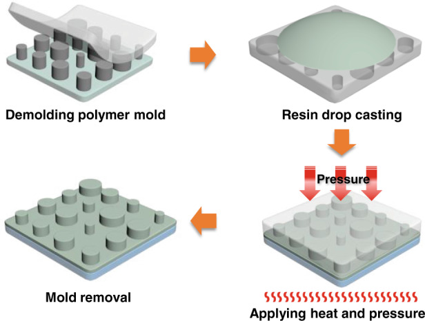
Schematic of metasurface fabrication by nanocomposite printing
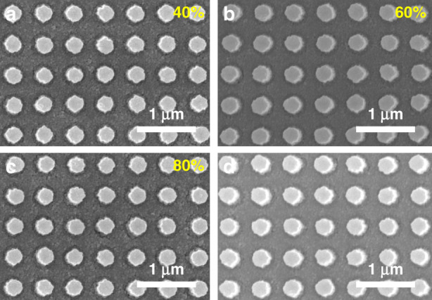
The effects of temperature and humidity on the PER nanostructures are evaluated, as the base resin of the PER is a polymer that is sensitive to heat. A uniform array of similar cylindrical PER nanostructures constitutes the PER metasurfaces for the tests (Fig. 2a), and the deformation of the nanostructures is assessed after annealing for 4 h at different temperatures (Fig. 2b–f). The PER nanostructures begin to collapse when the temperature exceeds 90 °C, which is the glass transition temperature of DPHA. We believe that the thermal resistance of the PER could be enhanced by using other base resins with higher glass transition temperatures. The same metasurfaces are also used for humidity tests where the metasurface is exposed to different relative humidities in a humidity-controlled chamber (Fig. 3a–c). The humidity test verifies that the PER nanostructures are not affected by the surrounding humidity even if the sample is immersed in water (Fig. 3d).
Fig. 2. Effect of temperature on PER nanostructures.

a Original PER nanostructures. b–f PER nanostructures after 4 h of annealing at different temperatures at a surrounding humidity of 30%. The PER patterns begin to collapse above 90 °C, which corresponds to the glass transition temperature of the base resin
Fig. 3. Effect of humidity on PER nanostructures. The test sample is identical to that of the temperature test.
a–c PER nanostructures after 4 h in a humidity-controlled chamber. d PER nanostructures after soaking in water. The PER nanostructures are not affected by the surrounding humidity
It is required to arrange the nanostructures according to phase for the visualization of the hologram. To design appropriate nanostructures, the refractive index and extinction coefficient of the TiO2 PER are evaluated for various nanoparticle concentrations (Fig. 4a). A higher concentration results in a higher refractive index and extinction coefficient. By spin-coating and curing the PER, a uniform thin film is formed (Fig. 4b). The refractive index and extinction coefficient of the PER are measured using ellipsometry (Fig. S2). When the concentration of TiO2 PER is adjusted, 89 wt% PER shows a higher refractive index than 80 wt% PER, confirming that it is sufficiently applicable to other wavelength bands (Fig. 4c, d). A finite-difference time-domain (FDTD) simulation is performed based on the measured refractive index and extinction coefficient to optimize the hologram formation of the green and red lights. The height, period, and diameter of the cylindrical nanostructures are determined to achieve a transmission phase delay from 0 to 2π. The FDTD simulation reveals that 80 wt% TiO2 PER is suitable for green light and 89 wt% TiO2 PER is suitable for red light (Fig. 4e, f). When the diameter of the nanostructure is varied from 150 to 380 nm, the TiO2 PER can achieve the required phase shift for each λ by changing the concentration.
Fig. 4. Optical properties of TiO2 PER thin films.

a Refractive index (dashed lines) and extinction coefficient (solid lines) according to TiO2 nanoparticle concentration following solvent removal. b SEM image of a spin-coated 80% TiO2 nanoparticle layer on a glass substrate. Optical properties of TiO2 PER thin films: (c) measured refractive index and extinction coefficient and (d) simulated transmission of 80 wt% PER. The transmission is simulated at λ = 532 nm. e Refractive index and (f) simulated transmission of 89 wt% PER. The transmission is simulated at λ = 635 nm
To design the metahologram, we use the Gerchberg-Saxton (GS) algorithm, which employs an iteration process to reduce the error between the desired and holographic images. The desired grayscale image is represented by a two-dimensional matrix consisting of the target intensity distribution intensities from 0 to 255. The complex amplitude profile in the object plane can be obtained by taking the inverse Fourier transform of the target image. Then, the magnitude of the transformed matrix is normalized by the GS algorithm so that the matrix contains phase information only. The Fourier transform of the consequent matrix represents the holographic image generated by a metasurface when it is encoded by the phase-only profile. However, the image has large errors compared with the desired image, so the magnitude of the image is normalized again and multiplied by the desired image. This process enforces the reduction of the error during the iteration process. After taking the inverse Fourier transform again, those processes are iterated. When the error becomes sufficiently small, the normalized phase-only matrix at the object plane is the phase profile required for a metasurface to produce the desired image.
The metasurface consists of eight types of cylindrical nanostructures with diameters that vary from 150 to 380 nm, with a periodicity of 500 nm and height of 800 nm (Fig. 5a). The polymer soft mold has a hole-shaped pattern that is the inverse of the master stamp. The SEM images of the h-PDMS verify that the master stamp is replicated effectively, without any loss of the desired pattern (Fig. 5b). Furthermore, the nanostructures of the master stamp are successfully replicated with the TiO2 PER (Fig. 5c, d). Although the pattern is composed of nanoparticles, it is uniform and smooth as a result of the small average diameter of the TiO2 nanoparticles of 27.3 nm, which is small compared to that of the pattern size (Fig. S1).
Fig. 5. Scanning electron microscopy (SEM) images.
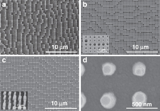
a Si master stamp, b h-PDMS polymer replica. c, d TiO2 80% nanoparticle PER nanostructures
The designed metahologram is fabricated using TiO2 PER, and the holographic image is observed by shining lasers of λ = 532 and 635 nm (Fig. 6). When λ = 532 nm, the 80 wt% PER yields the clearest image (Fig. 6b). When λ = 635 nm, the 89 wt% PER yields the clearest image (Fig. 6h). Figure 7 depicts the hologram efficiency, which is the optical power ratio of the incident light to the holographic image. The maximum efficiency is 48% at λ = 532 nm and 35% at λ = 635 nm. The FDTD simulation and experimental values are consistent, but the efficiency of the fabricated metahologram is lower than the FDTD simulation result because of fabrication defects. The transmission coefficients of the metasurfaces are affected by the physical shapes of the individual nanostructures, but the metasurfaces in this work have several kinds of defects, such as slanted sidewalls and random deformation (Fig. S3).
Fig. 6. Captured holographic images produced by TiO2 PER metaholograms with different concentrations.

Measurement results at λ = 532 nm with concentrations of (a) 67 wt%, (b) 80 wt%, (c) 86 wt%, and (d) 89 wt% and at λ = 635 nm with concentrations of (e) 67 wt%, (f) 80 wt%, (g) 86 wt%, and (h) 89 wt%. i Measured hologram efficiency according to TiO2 PER concentration
Fig. 7.
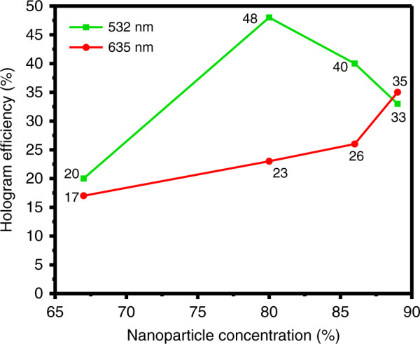
Measured hologram efficiency according to TiO2 PER concentration
NIL is a solution-based and direct-contact type of lithography. As the replicated mold is flexible, patterns can easily be printed on various substrates. In addition to flat glass, the patterns can be formed on flexible and curved glass substrates (Fig. 8). Although the clarity is reduced owing to the phase deviation resulting from the substrate curvature, the hologram can be easily recognized. Moreover, less distortion of the structure occurs on substrates with higher curvatures than other lithography types. Therefore, our approach can be applied to create metasurfaces on curved substrates.
Fig. 8. Captured holographic images generated from TiO2 PER metaholograms.

They are fabricated on (a) and (d) flat, (b) and (e) flexible, and (c) and (f) curved substrates. Metaholograms following the durability test: (g) SEM image and (h) generated hologram after 24 h at 70 °C and 70% humidity
A reliability test is again conducted in a high-temperature and high-humidity environment to verify the durability of the PER metasurfaces that are produced through the solution-based NIL process. The metasurfaces are stored for 24 h in an atmosphere of 70% humidity at 70 °C. The SEM images confirm that the nanostructures are not deformed (Fig. 8g). The PER synthesized in this study was stable in high-temperature and high-humidity environments. Figure 8h depicts a holographic image following the reliability test. Moreover, the conversion efficiency of the metahologram is 43% after the test. No significant performance degradation occurs compared to the efficiency of 48% before the reliability test.
Discussion
There have been various reported works on monolithic TiO2 metasurfaces, allowing for comparison. In the case of polarization-insensitive metasurfaces, a transmittance of 83% at a wavelength of 532 nm has been proven58. The efficiency of the monolithic metasurfaces is higher than that of TiO2 PER metasurfaces in this work because the refractive index of TiO2 is much higher than that of TiO2 PER. However, it is expensive and time-consuming to fabricate monolithic TiO2 metasurfaces because they require challenging processes, such as the atomic layer deposition of TiO2 over 500 nm. In contrast, our TiO2 PER metasurfaces can be rapidly fabricated at very low cost once a master mold is prepared. Moreover, TiO2 PER metasurfaces can be defined for any kind of substrate, including flexible polymers and curved glass, which are not compatible with typical monolithic TiO2 metasurfaces.
In this study, although it is necessary to produce a master stamp using electron beam lithography, a high-efficiency metahologram is produced through a semipermanently usable master stamp. By producing reusable polymer molds using h-PDMS with excellent mechanical strength, metasurfaces can be replicated repeatedly with a low cost. The TiO2 PER, which has a high refractive index, is synthesized and applied in the production of metaholograms. Furthermore, the concentration is optimized to control the refractive index of the PER. Using the solution-based NIL process, it is possible to create metasurfaces on flexible and curved substrates. The reliability test validates that the PER metasurfaces maintain their optical performance at temperatures below the glass transition temperature of the base resin. The surrounding humidity does not influence the PER metasurface. As high fabrication cost is a major limitation in the metasurface field, this low-cost and high-efficiency NIL-based manufacturing method may provide a breakthrough in the commercialization of metasurfaces.
Supplementary information
Acknowledgements
H.L. acknowledges the financial supports from the Technology Innovation program (20000887, Development of self-healing impact resistant film coating material and process technology for rollable displays) funded by the Ministry of Trade, Industry & Energy (MOTIE), and the International Research & Development program (NRF-2019K1A47A02113032) of the National Research Foundation (NRF) funded by the Ministry of Science and ICT (MSIT) of the Korean government. J.R. acknowledges the POSCO-POSTECH-RIST Convergence Research Center program funded by POSCO, the LGD-SNU incubation program funded by LG Display, and the NRF grants (NRF-2022M3C1A3081312, CAMM-2019M3A6B3030637, NRF-2019R1A5A8080290) funded by the MSIT of the Korean government. J.K. acknowledges the POSTECH Alchemist fellowship. Y.K. acknowledges the Hyundai Motor Chung Mong-Koo fellowship, and the NRF Ph.D. fellowship (NRF-2022R1A6A3A13066251) funded by the Ministry of Education of the Korean government.
Author contributions
W.K., G.Y. and J.K. contributed equally to this work. J.R. conceived the idea and initiated the project. W.K., J.K., H.J. and H.C. performed the experiments. G.Y., Y.K. and T.B. performed simulations. G.Y., J.R. and W.K. wrote the manuscript. J.R. and H.L. supervised the project. All authors participated in the discussion and confirmed the final manuscript.
Competing interests
The authors declare no competing interests.
Footnotes
These authors contributed equally: Wonjoong Kim, Gwanho Yoon, Joohoon Kim
Contributor Information
Junsuk Rho, Email: jsrho@postech.ac.kr.
Heon Lee, Email: heonlee@korea.ac.kr.
Supplementary information
The online version contains supplementary material available at 10.1038/s41378-022-00403-0.
References
- 1.Keshavarz Hedayati M, Elbahri M. Review of metasurface plasmonic structural color. Plasmonics. 2017;12:1463–1479. doi: 10.1007/s11468-016-0407-y. [DOI] [Google Scholar]
- 2.Chen H-T, Taylor AJ, Yu N. A review of metasurfaces: physics and applications. Rep. Prog. Phys. 2016;79:076401. doi: 10.1088/0034-4885/79/7/076401. [DOI] [PubMed] [Google Scholar]
- 3.Xu W, Xie L, Ying Y. Mechanisms and applications of terahertz metamaterial sensing: a review. Nanoscale. 2017;9:13864–13878. doi: 10.1039/C7NR03824K. [DOI] [PubMed] [Google Scholar]
- 4.Ding F, Yang Y, Deshpande RA, Bozhevolnyi SI. A review of gap-surface plasmon metasurfaces: fundamentals and applications. Nanophotonics. 2018;7:1129–1156. doi: 10.1515/nanoph-2017-0125. [DOI] [Google Scholar]
- 5.Rho J. Metasurfaces: subwavelength nanostructure arrays for ultrathin flat optics and photonics. MRS Bull. 2020;45:180–187. doi: 10.1557/mrs.2020.68. [DOI] [Google Scholar]
- 6.Kim J, et al. Geometric and physical configurations of meta-atoms for advanced metasurface holography. InfoMat. 2021;3:739–754. doi: 10.1002/inf2.12191. [DOI] [Google Scholar]
- 7.Liu Y, Ke Y, Luo H, Wen S. Photonic spin hall effect in metasurfaces: a brief review. Nanophotonics. 2017;6:51–70. doi: 10.1515/nanoph-2015-0155. [DOI] [Google Scholar]
- 8.Bukhari SS, Vardaxoglou J, Whittow W. A metasurfaces review: definitions and applications. Appl. Sci. 2019;9:2727. doi: 10.3390/app9132727. [DOI] [Google Scholar]
- 9.Alaee R, Albooyeh M, Rockstuhl C. Theory of metasurface based perfect absorbers. J. Phys. D: Appl. Phys. 2017;50:503002. doi: 10.1088/1361-6463/aa94a8. [DOI] [Google Scholar]
- 10.Keshavarz Hedayati M, Elbahri M. Antireflective coatings: conventional stacking layers and ultrathin plasmonic metasurfaces, a mini-review. Materials. 2016;9:497. doi: 10.3390/ma9060497. [DOI] [PMC free article] [PubMed] [Google Scholar]
- 11.Jung C, et al. Metasurface-driven optically variable devices. Chem. Rev. 2021;121:13013–13050. doi: 10.1021/acs.chemrev.1c00294. [DOI] [PubMed] [Google Scholar]
- 12.Kamali SM, Arbabi E, Arbabi A, Horie Y, Faraon A. Highly tunable elastic dielectric metasurface lenses. Laser Photonics Rev. 2016;10:1002–1008. doi: 10.1002/lpor.201600144. [DOI] [Google Scholar]
- 13.Yu YF, et al. High-transmission dielectric metasurface with 2π phase control at visible wavelengths. Laser Photonics Rev. 2015;9:412–418. doi: 10.1002/lpor.201500041. [DOI] [Google Scholar]
- 14.Ding X, et al. Ultrathin Pancharatnam–Berry metasurface with maximal cross-polarization efficiency. Adv. Mater. 2015;27:1195–1200. doi: 10.1002/adma.201405047. [DOI] [PubMed] [Google Scholar]
- 15.Moon S-W, Kim Y, Yoon G, Rho J. Recent progress on ultrathin metalenses for flat optics. iScience. 2020;23:101877. doi: 10.1016/j.isci.2020.101877. [DOI] [PMC free article] [PubMed] [Google Scholar]
- 16.Yoon G, Jang J, Mun J, Nam KT, Rho J. Metasurface zone plate for light manipulation in vectorial regime. Commun. Phys. 2019;2:156. doi: 10.1038/s42005-019-0258-x. [DOI] [Google Scholar]
- 17.Badloe T, Kim I, Kim Y, Kim J, Rho J. Electrically tunable bifocal metalens with diffraction-limited focusing and imaging at visible wavelengths. Adv. Sci. 2021;8:2102646. doi: 10.1002/advs.202102646. [DOI] [PMC free article] [PubMed] [Google Scholar]
- 18.Zheng G, et al. Metasurface holograms reaching 80% efficiency. Nat. Nanotechnol. 2015;10:308–312. doi: 10.1038/nnano.2015.2. [DOI] [PubMed] [Google Scholar]
- 19.Wen D, et al. Helicity multiplexed broadband metasurface holograms. Nat. Commun. 2015;6:8241. doi: 10.1038/ncomms9241. [DOI] [PMC free article] [PubMed] [Google Scholar]
- 20.Ni X, Kildishev AV, Shalaev VM. Metasurface holograms for visible light. Nat. Commun. 2013;4:2807. doi: 10.1038/ncomms3807. [DOI] [Google Scholar]
- 21.Li L, et al. Electromagnetic reprogrammable coding-metasurface holograms. Nat. Commun. 2017;8:197. doi: 10.1038/s41467-017-00164-9. [DOI] [PMC free article] [PubMed] [Google Scholar]
- 22.Yoon G, Lee D, Nam KT, Rho J. “Crypto-display” in dual-mode metasurfaces by simultaneous control of phase and spectral responses. ACS Nano. 2018;12:6421–6428. doi: 10.1021/acsnano.8b01344. [DOI] [PubMed] [Google Scholar]
- 23.Yoon G, et al. Wavelength-decoupled geometric metasurfaces by arbitrary dispersion control. Commun. Phys. 2019;2:129. doi: 10.1038/s42005-019-0232-7. [DOI] [Google Scholar]
- 24.Ren H, et al. Complex-amplitude metasurface-based orbital angular momentum holography in momentum space. Nat. Nanotechnol. 2020;15:948–955. doi: 10.1038/s41565-020-0768-4. [DOI] [PubMed] [Google Scholar]
- 25.Kim I, et al. Dual-band operating metaholograms with heterogeneous meta-atoms in the visible and near-infrared. Adv. Opt. Mater. 2021;9:2100609. doi: 10.1002/adom.202100609. [DOI] [Google Scholar]
- 26.Naveed MA, et al. Optical spin-symmetry breaking for high-efficiency directional helicity-multiplexed metaholograms. Microsyst. Nanoeng. 2021;7:5. doi: 10.1038/s41378-020-00226-x. [DOI] [PMC free article] [PubMed] [Google Scholar]
- 27.Kim J, et al. Photonics encryption platform via dual-band vectorial metaholograms in the ultraviolet and visible. ACS Nano. 2022;16:3546–3533. doi: 10.1021/acsnano.1c10100. [DOI] [PubMed] [Google Scholar]
- 28.Naveed MA, et al. Novel spin-decoupling strategy in liquid crystal-integrated metasurfaces for interactive metadisplays. Adv. Opt. Mater. 2022;10:2200196. doi: 10.1002/adom.202200196. [DOI] [Google Scholar]
- 29.Kim, J. et al. Metasurface holography reaching the highest efficiency limit in the visible via one-step nanoparticle-embedded-resin printing. Laser Photonics Rev.16, 2200098 (2022).
- 30.Orazbayev B, Mohammadi Estakhri N, Beruete M, Alù A. Terahertz carpet cloak based on a ring resonator metasurface. Phys. Rev. B. 2015;91:195444. doi: 10.1103/PhysRevB.91.195444. [DOI] [Google Scholar]
- 31.Yang Y, et al. Full-polarization 3D metasurface cloak with preserved amplitude and phase. Adv. Mater. 2016;28:6866–6871. doi: 10.1002/adma.201600625. [DOI] [PubMed] [Google Scholar]
- 32.Sun S, et al. All-dielectric full-color printing with TiO2 metasurfaces. ACS Nano. 2017;11:4445–4452. doi: 10.1021/acsnano.7b00415. [DOI] [PubMed] [Google Scholar]
- 33.Badloe T, et al. Liquid crystal-powered Mie resonators for electrically tunable photorealistic color gradients and dark blacks. Light Sci. Appl. 2022;11:118. doi: 10.1038/s41377-022-00806-8. [DOI] [PMC free article] [PubMed] [Google Scholar]
- 34.Lee T, et al. Nearly perfect transmissive subtractive coloration through the spectral amplification of Mie scattering and lattice resonance. ACS Appl. Mater. Interfaces. 2021;13:26299–26307. doi: 10.1021/acsami.1c03427. [DOI] [PubMed] [Google Scholar]
- 35.Cheng F, Gao J, Luk TS, Yang X. Structural color printing based on plasmonic metasurfaces of perfect light absorption. Sci. Rep. 2015;5:11045. doi: 10.1038/srep11045. [DOI] [PMC free article] [PubMed] [Google Scholar]
- 36.Colburn S, Zhan A, Majumdar A. Metasurface optics for full-color computational imaging. Sci. Adv. 2018;4:eaar2114. doi: 10.1126/sciadv.aar2114. [DOI] [PMC free article] [PubMed] [Google Scholar]
- 37.Jang J, et al. Full and gradient structural colouration by lattice amplified gallium nitride Mie-resonators. Nanoscale. 2020;12:21392–21400. doi: 10.1039/D0NR05624C. [DOI] [PubMed] [Google Scholar]
- 38.Jang J, et al. Spectral modulation through the hybridization of Mie-scatterers and quasi-guided mode resonances: realizing full and gradients of structural color. ACS Nano. 2020;14:15317–15326. doi: 10.1021/acsnano.0c05656. [DOI] [PubMed] [Google Scholar]
- 39.Kim I, et al. Stimuli-responsive dynamic metaholographic displays with designer liquid crystal modulators. Adv. Mater. 2020;32:2004664. doi: 10.1002/adma.202004664. [DOI] [PubMed] [Google Scholar]
- 40.Kim I, et al. Holographic metasurface gas sensors for instantaneous visual alarms. Sci. Adv. 2021;7:eabe9943. doi: 10.1126/sciadv.abe9943. [DOI] [PMC free article] [PubMed] [Google Scholar]
- 41.Yoon, G. et al. Electrically tunable metasurface perfect absorber for infrared frequencies. Nano Converg.4, 36 (2017). [DOI] [PMC free article] [PubMed]
- 42.Kim I, et al. Pixelated bifunctional metasurface-driven dynamic vectorial holographic color prints for photonic security platform. Nat. Commun. 2021;12:3614. doi: 10.1038/s41467-021-23814-5. [DOI] [PMC free article] [PubMed] [Google Scholar]
- 43.So S, Badloe T, Noh J, Bravo-Abad J, Rho J. Deep learning enabled inverse design in nanophotonics. Nanophotonics. 2020;9:1041–1057. doi: 10.1515/nanoph-2019-0474. [DOI] [Google Scholar]
- 44.So S, Mun J, Rho J. Simultaneous inverse design of materials and structures via deep learning: demonstration of dipole resonance engineering using core–shell nanoparticles. ACS Appl. Mater. Interfaces. 2019;11:24264–24268. doi: 10.1021/acsami.9b05857. [DOI] [PubMed] [Google Scholar]
- 45.So S, Park N, Lee HJ, Rho J. New trends in nanophotonics. Nanophotonics. 2020;9:983–985. doi: 10.1515/nanoph-2020-0170. [DOI] [Google Scholar]
- 46.So S, Rho J. Designing nanophotonic structures using conditional deep convolutional generative adversarial networks. Nanophotonics. 2019;8:1255–1261. doi: 10.1515/nanoph-2019-0117. [DOI] [Google Scholar]
- 47.Yoon G, Kim I, Rho J. Challenges in fabrication towards realization of practical metamaterials. Microelectron. Eng. 2016;163:7–20. doi: 10.1016/j.mee.2016.05.005. [DOI] [Google Scholar]
- 48.Tseng AA, Chen K, Chen CD, Ma KJ. Electron beam lithography in nanoscale fabrication: recent development. IEEE Trans. Electron. Packag. Manuf. 2003;26:141–149. doi: 10.1109/TEPM.2003.817714. [DOI] [Google Scholar]
- 49.Chang THP. Proximity effect in electron‐beam lithography. J. Vac. Sci. Technol. 1975;12:1271–1275. doi: 10.1116/1.568515. [DOI] [Google Scholar]
- 50.Bailey TC, et al. Step and flash imprint lithography: an efficient nanoscale printing technology. J. Photopolym. Sci. Technol. 2002;15:481–486. doi: 10.2494/photopolymer.15.481. [DOI] [Google Scholar]
- 51.Horák M, et al. Comparative study of plasmonic antennas fabricated by electron beam and focused ion beam lithography. Sci. Rep. 2018;8:9640. doi: 10.1038/s41598-018-28037-1. [DOI] [PMC free article] [PubMed] [Google Scholar]
- 52.Küpers H, et al. Surface preparation and patterning by nano imprint lithography for the selective area growth of GaAs nanowires on Si(111) Semicond. Sci. Technol. 2017;32:115003. doi: 10.1088/1361-6641/aa8c15. [DOI] [Google Scholar]
- 53.Kim I, et al. Outfitting next generation displays with optical metasurfaces. ACS Photonics. 2018;5:3876–3895. doi: 10.1021/acsphotonics.8b00809. [DOI] [Google Scholar]
- 54.Hong S-H, et al. Fabrication of sub-50 nm Au nanowires using thermally curing nanoimprint lithography. Electron. Mater. Lett. 2009;5:139–143. doi: 10.3365/eml.2009.12.139. [DOI] [Google Scholar]
- 55.Chou SY, Krauss PR, Renstrom PJ. Nanoimprint lithography. J. Vac. Sci. Technol. B. 1996;14:4129–4133. doi: 10.1116/1.588605. [DOI] [Google Scholar]
- 56.Yoon, G., Lee, D. & Rho, J. Demonstration of equal-intensity beam generation by dielectric metasurfaces. J. Vis. Exp. e59066 (2019). [DOI] [PubMed]
- 57.Guo LJ. Nanoimprint lithography: methods and material requirements. Adv. Mater. 2007;19:495–513. doi: 10.1002/adma.200600882. [DOI] [Google Scholar]
- 58.Khorasaninejad M, et al. Polarization-insensitive metalenses at visible wavelengths. Nano Lett. 2016;16:7229–7234. doi: 10.1021/acs.nanolett.6b03626. [DOI] [PubMed] [Google Scholar]
Associated Data
This section collects any data citations, data availability statements, or supplementary materials included in this article.