Abstract
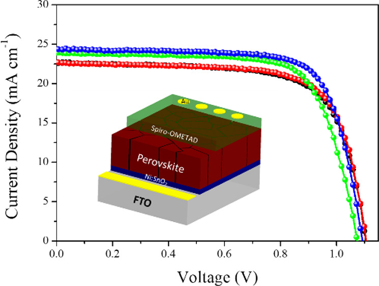
Perovskite solar cells (PSCs) based on a planar structure have recently become more attractive due to their simple manufacturing process and relatively low cost, while most perovskite solar cells employ highly porous TiO2 as an electron transport layer in mesoporous devices offering higher energy conversion efficiency (PCE). In planar structural devices, non-radiative recombination effects of the absorber layer and the electron transport layer cause potential loss and lower PCE. We created an efficient electron transport layer by combining low-temperature Ni-doped SnO2 with SDBS as a surfactant (denoted as Ni:SnO2). Doping Ni+ into low-temperature solution-processed SnO2 increased the power conversion efficiency of PSCs from 17.8 to 19.7%.
Introduction
The perovskite solar cells (PSCs) have been reported with rapid progress in power conversion efficiency, ranging from 3.8 to 25.5%, and have become prevalent in the past several years owing to their high efficiency, ease of manufacture, and low cost.1−5 Typically, PSCs with regular device configurations consist of a transparent electrode, an electron transport layer (ETL), a perovskite absorber, a hole transport layer, and a back contact electrode.6,7 In planar PSCs, the ETLs need to be very dense and smooth surfaces for electron extraction and hole blocking to prevent holes from absorbing layers from reaching transparent electrodes.8 Recently, numerous materials, such as TiO2, SnO2, ZnO, Zn2SnO4, WO3, etc., have been reported as ETLs. Among them, SnO2 can be used at low temperature (∼150 °C) and has exhibited better optical and electrical properties, band ailment to perovskite, and stability than the other materials, making it a strong candidate for highly efficient PSCs.9−12
Doping organic chemicals into ETLs either turns the Fermi level of the ETL to match the conduction band of the perovskite or modifies the perovskite/hole transport layers, thereby enhancing the crystallization and grain size of the perovskite layer.13−15 Consequently, doping is an effective and convenient approach to developing and improving both the perovskite and ETL by reducing the trap defects in the photo-absorber and ETL, which improves the separation of charge and transfer for the efficient performance of perovskite solar cells.
In 2016, Xiong et al. reported that magnesium-doped SnO2 as ETL layers lowered the levels of the conduction band, improved the interfacial contact, dramatically reduced the free electron density, and enhanced the cell’s PCE to 14.55%.16 Moreover, Ren and colleagues developed effective ETLs using a low-temperature process with a niobium dopant and found that a high PCE of 17.57% of Nb-doped SnO2-based devices originated from better surface morphology to increased electron mobility, enhanced electron extraction, and electrical conductivity.17 In addition, lithium-doped, gallium-doped, antimony-doped, and yttrium-doped SnO2 ETLs have also been investigated.18−21
It is evident that doping ETLs with metal aliovalent cations is an effective approach for enhancing the properties of ETLs and improving the PCEs of devices. However, very few studies have been conducted on Ni-doped SnO2 ETLs for perovskite solar cells. Previous studies of Ni-doped SnO2 have been devoted to improving the photocatalytic properties, resulting in a narrower optical bandgap owing to the substitution of Sn sites by Ni+ ions in SnO2.22 Ni+ cations can penetrate into the SnO2 lattice and substitute Ti cations. In addition, the Ni-doped SnO2 chemical co-precipitation approach decreases the average particle size of the nanoparticles with increasing amounts of doping Ni, which is expected to result in a smoother surface of the ETL in PSCs.23 Generally, Ni+-doped SnO2 ETLs are expected to further improve the photovoltaic performance of PSCs compared with other doped ETLs.
In a previous study, we demonstrated that electron transport in SnO2 can be effectively enhanced with surfactant sodium dodecylbenzene sulfonate (SDBS) at a low concentration.24 In this work, we describe how we developed an ideal Ni-doped SnO2 as an ETL by combining SnO2 with the SDBS surfactant. The PCE of the Ni:SnO2-based device improved from 17.8 to 19.7%, compared to commercial SnO2. Better electron mobility, greater electrical conductivity, and quicker electron extraction are the features that have improved the optical and electrical properties of the electron transport layer.
Results and Discussion
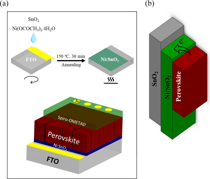
The SnO2 ETLs were spin-coated with SnO2 precursor solution at ambient temperature and then thermally annealed in air for 30 min at 150 °C. Figure 1a represents the SnO2 ETL fabrication method as well as the device structure of planar PSCs that uses undoped or doped SnO2 to collect and transport electrons from the absorber layer to the TCO. The Ni:SnO2 ETL was prepared by directly dissolving Ni(OCOCH3)2·4H2O in a commercially available SnO2 colloidal solution. A two-step deposition process was then used to create the perovskite layers. Figure 1b shows that a band diagram of the cell structure with the conduction band (CB) of ETL SnO2 nanocrystals was estimated from the band structure of the semiconductor, indicating as
| 1 |
where WS is the work function (4.36 eV) and VBM is the valance band maximum (3.74 eV).3
Figure 1.
(a) Schematic drawing illustrating the perovskite solar cell device structure based on the Ni:SnO2 ETL. (b) Energy-level diagram of the SnO2- or Ni:SnO2-based solar cells.
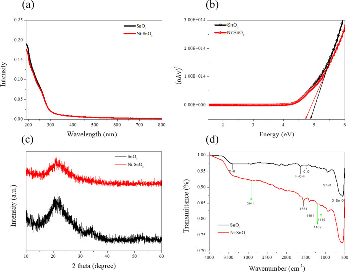
Figure 2a and Figure 2b illustrate the absorbance and estimated bandgap of two different ETL substrates, respectively, by UV–vis measurements. It can also be estimated that both the SnO2 and Ni:SnO2 films exhibit a good band alignment. Figure S1a, Supporting Information illustrates the transmission spectra of SnO2 and Ni:SnO2 at different concentrations, which indicates excellent transmittance in the visible region. Figure S1b, Supporting Information presents the optical image of the SnO2 precursor solution with different doping ratios of Ni+, which changes the solution from transparent to bluish-white, confirming the reduction in the transmittance of the ETL layer in Figure S1a. The XRD patterns of the SnO2 and Ni:SnO2 layers are shown in Figure 2c, demonstrating that the ETLs generated by Ni:SnO2 and SnO2 are comparable, indicating that Ni+ was doped entirely in the lattice of SnO2.
Figure 2.
(a) Optical transmission data of pristine SnO2 and Ni:SnO2 substrates. (b) Relation between (αhν)2 and photon energy hν of the control sample and Ni:SnO2 sample. (c) XRD patterns of the SnO2 and Ni:SnO2 layer. (d) FTIR analysis of the SnO2 layer and Ni:SnO2 layer.
The FTIR spectrum recorded from 400 to 4000 cm–1 to evaluate the bonding of SnO2 and Ni+ in the ETL film is shown in Figure 2d. The SDBS peaks at 2911, 1182, and 1119 cm1 confirm that SDBS was also integrated into the SnO2 film.25 In addition, the peaks at ∼930, ∼610, and ∼540 cm–1 are assigned to stretching of Sn–O and vibrations of O–Sn–O.26,27 The most remarkable differences between the two curves are the positions at 1561 and 1401 cm–1. Moreover, Figure S2, Supporting Information shows the increase in the relative intensity peaks of nickel-doped samples, implying the incorporation of Ni+ into the SnO2 lattice.28,29
Compact SnO2 films were spin-coated onto FTO substrates using a colloid dispersion solution with or without Ni+ doping. Atomic force microscopy (AFM) was used to investigate the surface morphology of the coated films. As shown in Figure 3a,b, both the ETL films indicate a smooth surface; however, the roughness of the Ni:SnO2 film (23.15 nm) is larger than that of SnO2 ETLs (22.63 nm), which is consistent with the surface morphology observed by scanning electron microscopy (SEM) in Figure 3c,d. When the mass concentration of Ni+ exceeded 1 mg mL–1, Ni:SnO2 aggregated into large particles, which could not form a smooth and dense ETL layer in Figure S3, Supporting Information.
Figure 3.
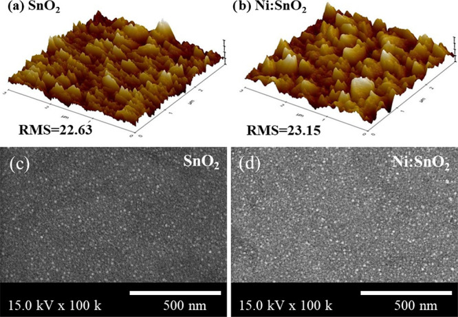
(a, b) AFM images of the SnO2 and Ni:SnO2 layer. (c, d) Top-view SEM images of SnO2 and Ni:SnO2 films coated on the pure TCO substrates.
The root-mean-square (RMS) roughnesses of perovskite films obtained from AFM deposited on SnO2 and Ni:SnO2 are 31.8 and 23.25 nm, respectively, indicating that the SnO2-modified perovskite is smoother in Figure 4a,b. Figure 4c,d shows the SEM pictures of the absorber layer coated onto different ETLs, confirming the surface morphology of the perovskite layers. Moreover, it was found that the perovskite coated on Ni:SnO2 was larger than that coated on the SnO2 layer. Simultaneously, the effects of different concentrations of Ni+ into SnO2 colloidal solution on the surface morphology of perovskite layers were also obtained, as shown in Figure S4, Supporting Information.
Figure 4.
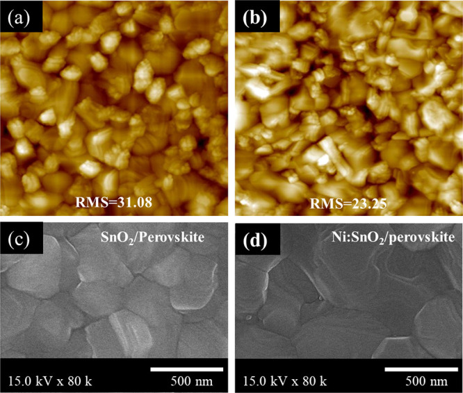
(a, b) Perovskite films grown on the SnO2 or Ni:SnO2 layer. (c, d) Top-view SEM pictures of absorber substrates grown onto the pristine control layer and doped SnO2 layer.
High-quality perovskite films are a precondition for the high efficiency of planar and mesoporous PSCs. The wetting surface of the ETL layers could assist in the formation of large-grain perovskite films owing to the smooth surface and suitable contact angle of the coated solution.5,30,31 The contact angle values of the two different ETL films are shown in Figure S5, Supporting Information. The contact angle measurement indicates that the increased concentration of the doped element Ni+ in the Ni:SnO2 films reduces the contact angle on the surface. However, the contact angle increased when a high concentration of elemental doping over 1.0 mg mL–1 was employed. The contact angle value is a minimum of 4.2° on the surface of 1 mg mL–1 Ni:SnO2 films, which can result in lower surface energy and accelerated crystallization for the growth of the perovskite structure.
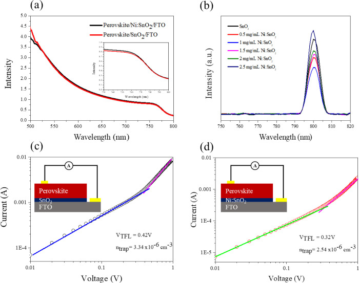
The light-harvesting properties of perovskites with various SnO2 and Ni:SnO2 ETLs were investigated using UV–vis spectroscopy (Figure 5a). Evidently, the Ni:SnO2 layer slightly influences the absorption ability of the perovskite layer. However, it is unchanged in its bandgap. The steady-state photoluminescence (PL) of the absorber formed onto various films is depicted in Figure 5b. The presence of SDBS reduced the PL intensity, indicating that the doped SnO2 film can extract electrons effectively from the absorber thin film. Figure 5c,d illustrates the I–V data of the perovskite layer with the structure of FTO/SnO2 (Ni:SnO2)/perovskite/Au. The bulk-trap density of the absorber formed onto control and doped SnO2 substrates was quantified using a space-charge-limited current measure, which was calculated using the equation below:
| 2 |
in which ε denotes the relative dielectric constant of the absorber layer (ε = 26), ε0 represents the vacuum permittivity (ε0 = 8.8 × 10⁻¹² F m–1), e denotes the electron charge (−1.6 × 10⁻¹⁹ C), L is the electrode distance, and VTFL symbolizes the trap-filled limit voltage calculated from the measured data. The absorber layer formed onto the pristine SnO2 substrate had a trap-state density of 3.34 × 1015 cm–3 and a VTFL of 0.42 V. Moreover, the trap-state density of the absorber formed onto the doped one was 2.54 × 1015 cm–3 with a VTLF of 0.32 V. Because of the lower grain boundaries of the absorber samples, this result suggests that Ni:SnO2 can effectively reduce the defect density of perovskite. The corresponding dark current–voltage (I–V) curves of SnO2 with different Ni+ concentrations are shown in Figure S6, Supporting Information. It is obvious that increasing the amount of Ni+ dopant to 2.5 mg mL–1 in the SnO2 substrate increased the trap densities of the perovskite layers from 2.54 × 10¹⁵ to 3.02 × 1015 cm–3. This increment originates from the rough surface of the perovskite caused by increased Ni+ at the grain boundaries and interfaces. Therefore, a Ni+ concentration of 1 mg mL–1 is optimal for high-quality perovskite formation.
Figure 5.
(a) UV–vis absorption data of absorber films with SnO2 and Ni:SnO2 layers (the inset is amplifying absorption spectra in the wavelength of 730–800 nm). (b) Steady-state PL of the absorber layers. SCLC measurements of electron-only devices based on (c) SnO2 and (d) Ni:SnO2 layers.
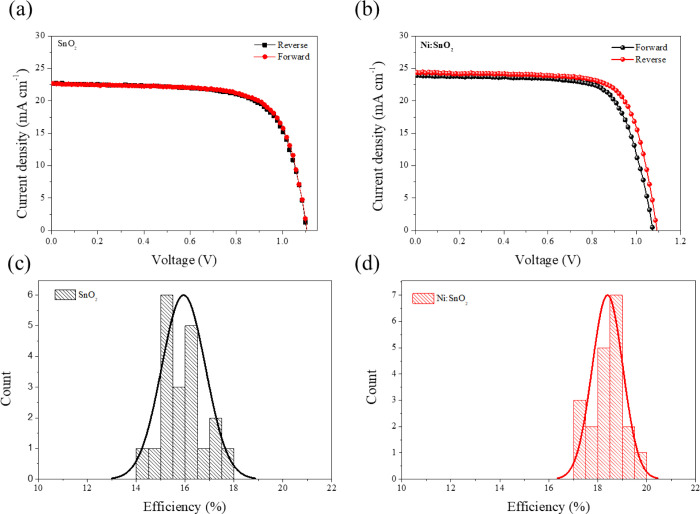
The J–V curves for SnO2- and Ni:SnO2-based devices in the reverse and forward scan directions are shown in Figure 6a,b and Figure S7, Supporting Information. The Ni:SnO2-based devices exhibiting high efficiency with the J–V characteristics of the champion devices utilizing ETLs are shown in Table 1 and Figure S2, Supporting Information. The maximum PCE of the devices based on the SnO2 ETL substrate is 17.7%, with the detailed parameters of Voc = 1.09 V, Jsc = 22.67 mA cm–2, and FF = 0.71. Remarkably, the optimal PCE can be increased to 19.7% by changing the control ETL to a Ni:SnO2 ETL, with detailed parameters of Voc and FF dramatically enhanced to 1.93 V and 0.74%, respectively. This result demonstrates that the Ni:SnO2 layer effectively passivated charge recombination at the ETL/perovskite interfaces, significantly inhibiting interfacial carrier recombination. To test the repeatability of the material and technique, we made 20 unique devices for each undoped and In-doped ETL, as shown in Table S2, Supporting Information. Figure 6c,d illustrates the distribution of device parameters, with the statistic parameters, which are listed in Figure S8, Supporting Information. For the doped SnO2-based devices, the J–V values clearly exhibit a tight distribution with a small standard deviation, suggesting remarkable repeatability.
Figure 6.
Current density–voltage (J–V) curves of devices based on (a) pristine SnO2 and (b) Ni:SnO2 under reverse-forward scanning directions. The PCE distribution of the PSCs of (c) SnO2 and (d) Ni:SnO2.
Table 1. Photovoltaic Parameters of Champion PSCs Based on SnO2 and Ni:SnO2 ETLs.
| VOC (V) | JSC (mA cm–2) | FF | PCE (%) | Rs (Ω) | Rsh (Ω) | ||
|---|---|---|---|---|---|---|---|
| SnO2 | reverse | 1.090 | 22.67 | 0.71 | 17.7 | 126.64 | 22529.07 |
| forward | 1.069 | 22.62 | 0.70 | 17.1 | 130.64 | 21719.86 | |
| Ni:SnO2 | reverse | 1.093 | 24.38 | 0.74 | 19.7 | 108.83 | 34398.75 |
| forward | 1.083 | 23.921 | 0.72 | 18.6 | 132.17 | 31149.95 | |
Conclusions
In conclusion, we successfully fabricated a low-temperature solution technique to effectively produce Ni:SnO2 as an ideal ETL for effective planar PSCs. The highest efficiency device exhibited a higher value of 19.7% under the same scan conditions compared to the control-based ETL. The exceptional efficiency of the perovskite solar cell based on Ni:SnO2 ETLs is primarily due to the smooth surface morphology and higher electron extraction. Furthermore, because of the low-temperature solution process, Ni:SnO2 improves the performance of perovskite solar cells.
Experimental Section
All reagents and chemicals were purchased from commercial suppliers without further purification. Tin dioxide(IV) and 15% hydrocolloid dispersion (SnO2) were purchased from Alfa Aesar. Nickel(II) acetate tetrahydrate (Ni(OCOCH3)2·4H2O, 99.995% trace metals basis), PbI2, spiro-OMeTAD (purity ≥99.8%), sodium dodecylbenzene sulfonate (SDBS), isopropanol (IPA), N,N-dimethylformamide (DMF), dimethyl sulfoxide (DMSO), chlorobenzene (CB), acetonitrile (ACN), 4-tert-butylpyridine (tBP), lithium bis(trifluoromethane sulfonyl)imide (Li-TFSI), and FK 209 Co(III) TFSI salts were from Sigma-Aldrich. Formamidinium iodide (FAI), methylammonium chloride (MACl), and methylammonium bromide (MABr) were obtained from GreatCell Solar.
Fabrication of SnO2 and Ni:SnO2 Films
SnO2 aqueous colloidal dispersion (1 mL) was dispersed into 4.65 mL of water containing 5.6 mg of the SDBS surfactant. The 1 mg Ni(OCOCH3)2·4H2O was dissolved in this solution and stirred at ambient temperature for 2 h. The SnO2 and Ni:SnO2 layers were formed at 3000 rpm for 30 s using the corresponding solution and then dried on a hot plate at 150 °C for 30 min to remove the residual solvent. Finally, the SnO2 and Ni:SnO2 films were obtained.
Fabrication of Solar Cells
The perovskite layers were spin-coated on different ETL substrates using a two-step deposition process. PbI2 (600 mg) was dissolved in 1 mL of DMF and DMSO (9:1, volume/volume) with stirring at 70 °C for 3 h. The PbI2 precursor solution was coated onto the SnO2 and Ni:SnO2 films at 2000 rpm for 20 s. The mixture including 60 mg of FAI, 6 mg of MABr, and 6 mg of MACl in 1 mL of IPA was coated onto the PbI2 substrates at 4000 rpm for 20 s (20 s loading time) and then heated at 150 °C for 20 min. Then, the spiro-OMeTAD solution (72.3 mg/mL) with tBP, FK 209 Co(III) TFSI, and Li-TFSI additive was spin-coated onto the perovskite layers. Au electrodes (100 nm) were thermally evaporated at a rate of 2 Å/s.
Characterization
The Fourier transform infrared (FTIR) spectra were recorded using an infrared spectrometric analyzer (Vertex 70, Bruker, Germany). SEM images were gained by field-emission scanning electron microscopy (S-4700, Japan) under an accelerating voltage of 15 kV. Steady-state photoluminescence (PL) spectra were performed on a QuantaMaster 50 PTI (USA). The J–V curves for PSCs were performed both at forward scan (from −0.1 to 2 V, step 0.02 V) and (from 2 to −0.1 V, step 0.02 V) using a solar simulator (Polaromix K201, Solar simulator LAB 50, McScience K3000) with an irradiance of 100 mW cm–2 (AM 1.5G). The absorption properties of the films were measured by a UV–vis spectrophotometer (Agilent 8453, USA). X-ray diffraction (XRD) patterns were recorded on an XRD Rigaku DMAX 2200 diffractometer with a Cu Kα anode (λ = 0.1542 nm) operating at 40 kV and 30 mA.
Acknowledgments
This work was supported by grants from the National Research Foundation of Korea (NRF), funded by the Ministry of Science and ICT (NRF-2020R1F1A1076576), the Korea Institute of Energy Technology Evaluation and Planning (KETEP), the Ministry of Trade, Industry & Energy (MOTIE) of the Republic of Korea (no. 20194030202290), and the Gachon University research fund of 2019 (GCU-2019-0800). We thank the Smart Materials Research Center for IoT (supported by the NFEC at Gachon University) for their support and assistance with the SEM.
Supporting Information Available
The Supporting Information is available free of charge at https://pubs.acs.org/doi/10.1021/acsomega.2c00965.
Additional experimental details, materials, and methods, including photographs of the experimental setup (PDF)
The authors declare no competing financial interest.
Supplementary Material
References
- Kojima A.; Teshima K.; Shirai Y.; Miyasaka T. Organometal halide perovskites as visible-light sensitizers for photovoltaic cells. J. Am. Chem. Soc. 2009, 131, 6050–6051. 10.1021/ja809598r. [DOI] [PubMed] [Google Scholar]
- Wang Y.; Li S.; Zhang P.; Liu D.; Gu X.; Sarvari H.; Ye Z.; Wu J.; Wang Z.; Chen Z. D. Solvent annealing of PbI2 for the high-quality crystallization of perovskite films for solar cells with efficiencies exceeding 18%. Nanoscale 2016, 8, 19654–19661. 10.1039/C6NR07076K. [DOI] [PubMed] [Google Scholar]
- Jiang Q.; Zhang L.; Wang H.; Yang X.; Meng J.; Liu H.; Yin Z.; Wu J.; Zhang X.; You J. Enhanced electron extraction using SnO2 for high-efficiency planar-structure HC(NH2)2PbI3-based perovskite solar cells. Nat. Energy 2016, 2, 1–7. 10.1038/nenergy.2016.177. [DOI] [Google Scholar]
- Zhao Y.; Zhu K. Organic–inorganic hybrid lead halide perovskites for optoelectronic and electronic applications. Chem. Soc. Rev. 2016, 45, 655–689. 10.1039/C4CS00458B. [DOI] [PubMed] [Google Scholar]
- Zhang H.; Azimi H.; Hou Y.; Ameri T.; Przybilla T.; Spiecker E.; Kraft M.; Scherf U.; Brabec C. J. Improved high-efficiency perovskite planar heterojunction solar cells via incorporation of a polyelectrolyte interlayer. Chem. Mater. 2014, 26, 5190–5193. 10.1021/cm502864s. [DOI] [Google Scholar]
- Shi Z.; Jayatissa A. H. Perovskites-based solar cells: A review of recent progress, materials and processing methods. Materials 2018, 11, 729. 10.3390/ma11050729. [DOI] [PMC free article] [PubMed] [Google Scholar]
- Lee M. M.; Teuscher J.; Miyasaka T.; Murakami T. N.; Snaith H. J. Efficient hybrid solar cells based on meso-superstructured organometal halide perovskites. Science 2012, 338, 643–647. 10.1126/science.1228604. [DOI] [PubMed] [Google Scholar]
- Mahmood K.; Sarwar S.; Mehran M. T. Current status of electron transport layers in perovskite solar cells: materials and properties. RSC Adv. 2017, 7, 17044–17062. 10.1039/C7RA00002B. [DOI] [Google Scholar]
- Quy H. V.; Truyen D. H.; Kim S.; Bark C. W. Reduced defects and enhanced performance of (FAPbI3)0.97(MAPbBr3)0.03-based perovskite solar cells by trimesic acid additives. ACS Omega 2021, 16151. 10.1021/acsomega.1c01909. [DOI] [PMC free article] [PubMed] [Google Scholar]
- Quy H. V.; Truyen D. H.; Kim S.; Bark C. W. Facile synthesis of spherical TiO2 hollow nanospheres with a diameter of 150 nm for high-performance mesoporous perovskite solar cells. Materials 2021, 14, 629. 10.3390/ma14030629. [DOI] [PMC free article] [PubMed] [Google Scholar]
- Wang J. T.-W.; Ball J. M.; Barea E. M.; Abate A.; Alexander-Webber J. A.; Huang J.; Saliba M.; Mora-Sero I.; Bisquert J.; Snaith H. J.; Nicholas R. J. Low-temperature processed electron collection layers of graphene/TiO2 nanocomposites in thin film perovskite solar cells. Nano Lett. 2014, 14, 724–730. 10.1021/nl403997a. [DOI] [PubMed] [Google Scholar]
- Wu Y.; Yang X.; Chen H.; Zhang K.; Qin C.; Liu J.; Peng W.; Islam A.; Bi E.; Ye F.; Yin M.; Zhang P.; Han L. Highly compact TiO2 layer for efficient hole-blocking in perovskite solar cells. Appl. Phys. Express 2014, 7, 052301 10.7567/APEX.7.052301. [DOI] [Google Scholar]
- Bahadur J.; Ghahremani A. H.; Martin B.; Druffel T.; Sunkara M. K.; Pal K. Solution processed Mo doped SnO2 as an effective ETL in the fabrication of low temperature planer perovskite solar cell under ambient conditions. Org. Electron. 2019, 67, 159–167. 10.1016/j.orgel.2019.01.027. [DOI] [Google Scholar]
- Ahmed A.; Riaz K.; Mehmood H.; Tauqeer T.; Ahmad Z. Performance optimization of CH3NH3Pb(I1-xBrx)3 based perovskite solar cells by comparing different ETL materials through conduction band offset engineering. Opt. Mater. 2020, 105, 109897 10.1016/j.optmat.2020.109897. [DOI] [Google Scholar]
- Aygüler M. F.; Hufnagel A. G.; Rieder P.; Wussler M.; Jaegermann W.; Bein T.; Dyakonov V.; Petrus M. L.; Baumann A.; Docampo P. Influence of fermi level alignment with tin oxide on the hysteresis of perovskite solar cells. ACS Appl. Mater. Interfaces 2018, 10, 11414–11419. 10.1021/acsami.8b00990. [DOI] [PubMed] [Google Scholar]
- Xiong L.; Qin M.; Yang G.; Guo Y.; Lei H.; Liu Q.; Ke W.; Tao H.; Qin P.; Li S.; Yu H.; Fang G. Performance enhancement of high temperature SnO2-based planar perovskite solar cells: electrical characterization and understanding of the mechanism. J. Mater. Chem. A 2016, 4, 8374–8383. 10.1039/C6TA01839D. [DOI] [Google Scholar]
- Ren X.; Yang D.; Yang Z.; Feng J.; Zhu X.; Niu J.; Liu Y.; Zhao W.; Liu S. F. Solution-processed Nb: SnO2 electron transport layer for efficient planar perovskite solar cells. ACS Appl. Mater. Interfaces 2017, 9, 2421–2429. 10.1021/acsami.6b13362. [DOI] [PubMed] [Google Scholar]
- Park M.; Kim J.-Y.; Son H. J.; Lee C.-H.; Jang S. S.; Ko M. J. Low-temperature solution-processed Li-doped SnO2 as an effective electron transporting layer for high-performance flexible and wearable perovskite solar cells. Nano Energy 2016, 26, 208–215. 10.1016/j.nanoen.2016.04.060. [DOI] [Google Scholar]
- Roose B.; Johansen C. M.; Dupraz K.; Jaouen T.; Aebi P.; Steiner U.; Abate A. A Ga-doped SnO2 mesoporous contact for UV stable highly efficient perovskite solar cells. J. Mater. Chem. A 2018, 6, 1850–1857. 10.1039/C7TA07663K. [DOI] [Google Scholar]
- Bai Y.; Fang Y.; Deng Y.; Wang Q.; Zhao J.; Zheng X.; Zhang Y.; Huang J. Low temperature solution-processed Sb: SnO2 nanocrystals for efficient planar perovskite solar cells. ChemSusChem 2016, 9, 2686–2691. 10.1002/cssc.201600944. [DOI] [PubMed] [Google Scholar]
- Yang G.; Lei H.; Tao H.; Zheng X.; Ma J.; Liu Q.; Ke W.; Chen Z.; Xiong L.; Qin P.; Chen Z.; Qin M.; Lu X.; Yan Y.; Fang G. Reducing hysteresis and enhancing performance of perovskite solar cells using low-temperature processed Y-doped SnO2 nanosheets as electron selective layers. Small 2017, 13, 1601769. 10.1002/smll.201601769. [DOI] [PubMed] [Google Scholar]
- Jiang F.; Peng L.; Liu T. Ni-doped SnO2 dilute magnetic semiconductors: Morphological characteristics and optical and magnetic properties. J. Supercond. Novel Magn. 2020, 33, 3051–3058. 10.1007/s10948-020-05533-y. [DOI] [Google Scholar]
- Aliahmad M.; Dehbashi M.. Ni-doped SnO2 nanoparticles synthesized by chemical co-precipitation method. J. Energy Environ. 2013, 4. [Google Scholar]
- Hoang V. Q.; Lee S. K.; Bark C. W. Dispersed SnO2 colloids using sodium dodecyl benzene sulfonate for high-performance planar perovskite solar cells. Sol. Energy 2021, 230, 747–753. 10.1016/j.solener.2021.10.081. [DOI] [Google Scholar]
- Wu X.; Liu J.; Wu D.; Zhao Y.; Shi X.; Wang J.; Huang S.; He G. Highly conductive and uniform graphene oxide modified PEDOT: PSS electrodes for ITO-free organic light emitting diodes. J. Mater. Chem. C 2014, 2, 4044–4050. 10.1039/C4TC00305E. [DOI] [Google Scholar]
- Amalric-Popescu D.; Bozon-Verduraz F. Infrared studies on SnO2 and Pd/SnO2. Catal. 2001, 70, 139–154. 10.1016/S0920-5861(01)00414-X. [DOI] [Google Scholar]
- Gundrizer T.; Davydov A. IR spectra of oxygen adsorbed on SnO2. React. Kinet. Catal. Lett. 1975, 3, 63–70. 10.1007/BF02216890. [DOI] [Google Scholar]
- Kandasamy M.; Seetharaman A.; Sivasubramanian D.; Nithya A.; Jothivenkatachalam K.; Maheswari N.; Gopalan M.; Dillibabu S.; Eftekhari A. Ni-doped SnO2 nanoparticles for sensing and photocatalysis. ACS Appl. Nano Mater. 2018, 1, 5823–5836. 10.1021/acsanm.8b01473. [DOI] [Google Scholar]
- Chen H.; Ding L.; Sun W.; Jiang Q.; Hu J.; Li J. Synthesis and characterization of Ni doped SnO2 microspheres with enhanced visible-light photocatalytic activity. RSC Adv. 2015, 5, 56401–56409. 10.1039/C5RA10268E. [DOI] [Google Scholar]
- Gong W.; Guo H.; Zhang H.; Yang J.; Chen H.; Wang L.; Hao F.; Niu X. Chlorine-doped SnO2 hydrophobic surfaces for large grain perovskite solar cells. J. Mater. Chem. C 2020, 8, 11638–11646. 10.1039/D0TC00515K. [DOI] [Google Scholar]
- Baena J. P. C.; Steier L.; Tress W.; Saliba M.; Neutzner S.; Matsui T.; Giordano F.; Jacobsson T. J.; Kandada A. R. S.; Zakeeruddin S. M. Highly efficient planar perovskite solar cells through band alignment engineering. Energy Environ. Sci. 2015, 8, 2928–2934. 10.1039/C5EE02608C. [DOI] [Google Scholar]
Associated Data
This section collects any data citations, data availability statements, or supplementary materials included in this article.


