

Abstract

In this research, solar cell capacitance simulator-one-dimensional (SCAPS-1D) software was used to build and probe nontoxic Cs-based perovskite solar devices and investigate modulations of key material parameters on ultimate power conversion efficiency (PCE). The input material parameters of the absorber Cs-perovskite layer were incrementally changed, and with the various resulting combinations, 63,500 unique devices were formed and probed to produce device PCE. Versatile and well-established machine learning algorithms were thereafter utilized to train, test, and evaluate the output dataset with a focused goal to delineate and rank the input material parameters for their impact on ultimate device performance and PCE. The most impactful parameters were then tuned to showcase unique ranges that would ultimately lead to higher device PCE values. As a validation step, the predicted results were confirmed against SCAPS simulated results as well, highlighting high accuracy and low error metrics. Further optimization of intrinsic material parameters was conducted through modulation of absorber layer thickness, back contact metal, and bulk defect concentration, resulting in an improvement in the PCE of the device from 13.29 to 16.68%. Overall, the results from this investigation provide much-needed insight and guidance for researchers at large, and experimentalists in particular, toward fabricating commercially viable nontoxic inorganic perovskite alternatives for the burgeoning solar industry.
1. Introduction
Machine learning (ML), a subfield of artificial intelligence (AI),1,2 utilizes the knowledge of mathematics, statistics, and computer science3 to build computer algorithms for specific aims. The algorithmic system learns from the experimental or computational data, analyzes it, and builds patterns to anticipate behavior with the goal to make better judgments. It is, therefore, no surprise that over the past decade, ML has become a vital tool in all branches of STEM. The field of Material Science has evolved in step during this time as well, allowing scientists to utilize a broad variety of model prediction methods and tools based on ML algorithms for use in different materials and devices.4−6 With the use of these tools, material scientists can now devise new ways of investigating materials’ characteristics and improving material performance in general. Generating data from a specific process or device followed by data wrangling, feature generation, feature engineering, constructing models, and eventually making choices to get optimum outputs7 are the steps in the ML processes.
Perovskites, a material family with a crystal structure analogous to the mineral ‘perovskite’, consisting of (CaTiO3),8 with the generalized formula ABX3 (where A represents cation species, e.g., CH3NH3, HC(NH2)2, Cs, etc.; B represents metal species, e.g., Sn, Pb, Ge, etc.; and X represents halide species9,10), have shown promising results for light capture, exciton production, and charge transition to corresponding device layers for extraction.11,12 Pb halide perovskites, particularly, have improved PCE from 3.8 to 25.2 percent in the last decade.13−15 The wide absorption range, high diffusion length, and excellent charge-carrier mobility of these Pb-based perovskites are remarkable. The perovskite material may be used alone as an absorber in different solar device designs and architectures, but it can also be utilized in conjunction with the standard silicon layer to lower the $/W value.16 While there are many benefits to using perovskite solar cells (PSCs), the toxicity and harmful consequences of Pb must be considered.17−19 Pb is leached and transported by water, air, and soil20 (Figure 1). Despite its excellent performance and durability,21,22 commercializing this technology on a wide scale poses substantial challenges.23 A broad range of nontoxic materials is currently being investigated for commercial feasibility using important device performance characteristics such as efficiency, stability, and degradability.24−26
Figure 1.

Schematic of environment pollution by Pb-based perovskites.
The current research utilizes supervised ML to critically investigate nontoxic perovskite devices (ABX3: A = Cs; B = Sn, Bi, Ge, Ag, and Sb and X = I, Br) and offers researchers clear guidance toward enhancing PCE values. Cs-based perovskites were particularly chosen given the fact that Cs can strongly tune the properties and performance of PSCs, in particular leading to higher device stability. This has been made clear through the fact that for the last few decades, researchers at large have strongly concentrated on the development of Cs-based perovskites with an aim to improve the stability, reproducibility, and spectral properties of PSCs.27 This focus on Cs has additionally been beneficial due to the nontoxic nature of the material.25,26 It is encouraging to see that experimental studies have been steadily showcasing this viability of Cs-based perovskite materials through stability and increasing PCE measurements.24
In the present research, solar cell capacitance simulator-one-dimensional (SCAPS-1D) was used for simulating single-junction Cs-perovskite (Figure 2 showcases a standard CsSnI3 structure) solar devices; the perovskite (absorber) parameters were modulated by incremental stages. A fairly large dataset consisting of the performance outputs from 63,500 unique devices was obtained. By utilizing the standard correlation algorithm together with a Random Forest algorithm, models were created and utilized to classify the properties of the material as a function of the highest impact on the performance and ultimate device PCE. The results from this investigation provide clear recommendations for researchers to selectively focus on and probe parameters that will impact device PCE the most, thereby providing a plausible pathway for disruption in the photovoltaic sector utilizing nontoxic inorganic perovskite materials.
Figure 2.
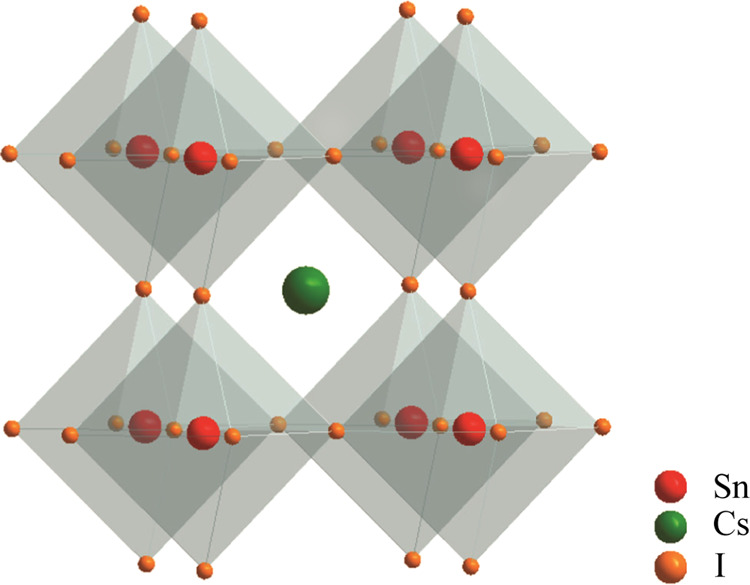
Crystal structure of CsSnI3.
2. Materials and Methodology
SCAPS-1D, devised by the University of Gent’s ELIS department,28−31 is used for our present work to simulate single-junction perovskite solar cells’ numerical simulations. SCAPS is a highly versatile software and is prolifically used within the photovoltaic community. It allows for a wide range of device architectures to be built and probed, utilizing the most realistic and accurate back-end physical equations to mimic fundamental photovoltaic activity such as light capture, exciton generation, charge transport, and recombination.
2.1. SCAPS Governing Equations and Definitions of Critical SCAPS Output Parameters
SCAPS solves three systems of equations for the carriers:32 transport, Poisson, and continuity. The following is the carrier continuity equation:
| 1 |
| 2 |
The electron–hole current densities, respectively, are denoted by Jn and Jp, the recombination and generation rates are denoted by R(x), G(x), respectively, and the position-dependent electron and hole concentrations, respectively, are denoted by p(x) and n(x). The drift-diffusion of electron–hole pairs is described by the following equations:
| 3 |
| 4 |
where μp and μn denote the electron and hole mobility, respectively, and Dn and Dp denote the electron and hole diffusion constants, respectively. SCAPS-1D solves the Poisson equation and continuity equations for electrons and holes together by taking the appropriate boundary conditions at the interfaces and contacts33 into consideration. The fill factor (FF) of the device is defined as follows:
| 5 |
where Vmp and Jmp represent the voltage and current density at the maximum power points. The short-circuit current density is denoted by Jsc, and the open-circuit voltage is denoted by Voc.
Defining how the aforementioned factors interact to produce the research’s primary result, notably device efficiency normalized to power input (Pin), is vital at this point
| 6 |
2.2. Device Structure
The solar device simulated in SCAPS and investigated in the present research is shown schematically in Figure 3. A conventional perovskite solar device consists of an antireflective coating, glass, a fluorine-doped tin oxide (FTO) electrode, an electron-transport layer (ETL), a perovskite layer, a hole transport layer (HTL), and an electrode layer.34 In the present research, the device layers constitute (glass/fluorine-doped tin oxide (FTO)/TiO2/Cs-based perovskite/Cu2O/Au). The noble metals Au, Ag, and Pt are commonly used as electrode materials.35 This type of structure significantly lowers electron–hole recombination and provides the necessary diffusion length for efficient electron–hole capture.36 In the perovskite layer, a maximum portion of the light is absorbed to create electron–hole pairs,35 and the rest of the light cannot be absorbed or converted to heat. As the electron and hole pairs are generated, they are transported through the electron-transport layer (ETL) and hole–transport layer (HTL) to generate electric current. The ETL extracts electrons from the perovskite layer and prevents electrons in the FTO from recombining with holes. TiO2 has been utilized as an ETL in most of the published perovskite solar devices.37 The HTL serves a similar purpose as the ETL, but for holes; in the current work, Cu2O acts as the standard device HTL. Glass and FTO layers are used to increase optical absorption for higher light absorption in the layers.38 However, typically, device performance only depends on the ETL, absorber, and HTL. Tables 1–3 list the material’s property values for each layer as utilized in this current research and used as input parameters into the SCAPS software. The SCAPS simulation settings were configured to make use of the specified spectrum of A.M. 1.5G at an operating temperature of 300 K.
Figure 3.

Schematic of the solar device structure utilized in SCAPS simulation.
Table 1. Cs-Based Lead-Free Perovskite Material Parameters.
| parameter | Cs2SnI6 | Cs3Bi2I9 | Cs2AgBiBr6 | CsSn0.5Ge0.5I3 | CsGeI3 | Cs3Sb2I9 | CsSnI3 | Cs2TiBr6 |
|---|---|---|---|---|---|---|---|---|
| bandgap (eV) | 1.48 | 2.03 | 2.05 | 1.5 | 1.6 | 2.05 | 1.3 | 1.6 |
| electron affinity | 4.3 | 3.4 | 4.19 | 3.9 | 3.52 | 3.65 | 3.5 | 4.47 |
| relative permittivity | 7.2 | 9.68 | 5.8 | 28 | 18 | 13.04 | 9.93 | 10 |
| conduction band DoS (cm–3) | 4.76 × 10¹⁸ | 4.98 × 10¹⁹ | 1 × 10¹⁹ | 1 × 10¹⁹ | 1 × 10¹⁸ | 4.33 × 10¹⁸ | 1 × 10¹⁹ | 1 × 10¹⁹ |
| valence band DoS (cm–3) | 4.6 × 10¹⁹ | 2.11 × 10¹⁹ | 1 × 10¹⁹ | 1 × 10¹⁹ | 1 × 10¹⁹ | 7.58 × 10¹⁸ | 1 × 10¹⁸ | 1 × 10¹⁹ |
| electron mobility (cm2/V.s) | 2.3 | 4.3 | 11.81 | 974 | 20 | 1.8 | 1500 | 4.4 |
| hole mobility (cm2/V.s) | 2.3 | 1.7 | 1.00 | 213 | 20 | 0.14 | 585 | 2.5 |
| donor concentration, Nd (cm–3) | 1 × 10⁹ | 1 × 10¹⁹ | 1 × 10⁹ | 1 × 10⁹ | 2 × 10¹⁶ | 1 × 10⁹ | 0 | 1 × 10¹⁹ |
| acceptor concentration, Na (cm–3) | 1 × 10⁹ | 1 × 10¹⁹ | 1 × 10⁹ | 1 × 10⁹ | 1 × 10⁹ | 1 × 10¹⁵ | 1 × 10¹⁹ |
Table 3. Parameters of ETL and HTL.
| parameter/layer | TiO2(ETL) | perovskite (absorber) | Cu2O(HTL) |
|---|---|---|---|
| layer thickness (nm) | 150 | 350 (static) | 150 |
| relative permittivity (εr) | 9 | 7–11 | 7.11 |
| bandgap energy (eV) | 3.2 | 1.5–1.7 | 2.17 |
| electron affinity (eV) | 4.26 | 4.15–4.30 | 3.2 |
| mobility of electron (cm2/V.s) | 20 | 20–100 | 200 |
| mobility of hole (cm2/V.s) | 10 | 20–100 | 80 |
| donor level concentration (Nd) (cm–3) | 1.0 × 10¹⁶ | 1.0 × 10⁹ (static) | 0 |
| acceptor level concentration (Na) (cm–3) | 0 | 1.0 × 10⁹ (static) | 1.0 × 10¹⁸ |
| conduction band DoS (Nc) (cm–3) | 2.2 × 10¹⁸ | 2.0 × 10¹⁸–1.0 × 10¹⁹ | 2.02 × 10¹⁷ |
| valence band DoS (Nv) (cm–3) | 1.8 × 10¹⁸ | 2.0 × 10¹⁸–1.0 × 10¹⁹ | 1.1 × 10¹⁹ |
| radiative recombination (cm3/s) | 2.3 × 10⁻⁹ | 2.3 × 10⁻⁹ (static) | 2.3 × 10⁻⁹ |
2.3. Simulation Parameters
The most fundamental parameters of each material layer utilized in the solar device for the current simulation are described below. These parameters are all material properties unique to each device layer, dependent on innate functionalities based on chemical composition, crystallographic orientation, etc.
-
1.
Thickness of the layers is optimized to fixed values to give maximum efficiency.39−41
-
2.
The bandgap of a material layer is related to its chemistry. It determines which portion of the electromagnetic (EM) spectrum is absorbed by the layers. Only photons having equal or higher than bandgap energy are absorbed.42 The ETL should have a high-energy bandgap to enable a considerable portion of the electromagnetic spectrum to flow through and reach the perovskite (absorber) layer.42
-
3.
Electron affinity: The perovskite (absorber) layer’s electron affinity is significant for the current investigation. To produce an electric current, the electron–hole pairs must be routed to the ETL and HTL. As the higher value of electron affinity means a larger barrier to moving electrons from the absorber to ETL, a minimal value of perovskite electron affinity is required.42
-
4.
Relative permittivity (or dielectric constant) measures how quickly a material polarizes in an electric field.43 The greater the value, the more likely it is to form exciton couples. As a result, we are more concerned with the absorber layer’s relative permittivity for our application.
-
5.
Conduction band density of states: In the perovskite and ETL, a larger DoS of the conduction band is preferable. This is a material feature that allows it to accept and conduct more electrons in the conduction band. Electrons will flow from the absorber’s (perovskite) conduction band to the ETL’s conduction band as soon as pairs of electron–hole are generated in the perovskite. Therefore, higher values of conduction band density of perovskites and ETL states have more influence on device PCE.42
-
6.
Valence band density of states: The holes will conduct from the perovskite’s valence band to the HTL’s valence band once they are formed. Higher valence band densities of perovskites and HTL states have more influence on device PCE.42
-
7.
Electron mobility: Maximal electron mobility is desired in both perovskites and ETLs. Once the electron–hole pairs are formed, the goal is to get the electrons out of the device as efficiently as possible (flow from perovskite → ETL → electrode).
-
8.
Hole mobility: same logic as #7 above. In this case, maximal hole mobility is desired in both perovskites and HTLs.
-
9.
Donor concentration: The concept of donor concentration originates in the doped semiconductor materials in favorable conditions. There, the addition of a specific dopant or impurity can add additional energy levels in the band alignment and provide a favorable passage of electrons to the conduction band. In an otherwise intrinsic system with no additional electron in the conductor band (which is the case for most moderate to high bandgap semiconductor materials), the concentration of electrons in the conduction band will be roughly equal to the donor concentration. This particular property can aid the transition and charge transfer in the perovskite/ETL interface further facilitating more carrier separation. However, for the HTL/perovskite interface, such energy levels in the band may facilitate the opposite effect. So, in an ideal perovskite solar device, the donor concentration on HTL is expected to be negligible. To maintain congruence with this idea, the donor concentration for the HTL in our input parameter in this simulation is kept at a null value.
-
10.
Acceptor concentration: The acceptor energy level takes electrons from the valence band or donates an electron to the conduction band, upon the addition of a dopant or an impurity. It is fundamentally related to the separatist that occurs at the ETL/perovskite interface. So, the value of acceptor concentration is taken from the experimental and previously reported literature on the topic.
-
11.
Absorption coefficient values: We have listed each material’s absorption coefficient vs light wavelength (400–700 nm). Also, we are more concerned with the perovskite (absorber) layer’s absorption coefficient as light absorption leads to exciton (electron–hole) couple generation.
-
12.
Recombination rate of electrons and holes: Recombination of electrons and holes can severely degrade the performance of solar devices. To maintain congruence with the previous investigations44,45 on the subject and experimental data, a reactive recombination coefficient of 2.3 × 10⁻⁹ cm3/s was considered in the bulk of perovskites. In addition, the effect of Auger recombination was considered to be negligible as the radiative mode of recombination significantly dominates Auger recombination.46−48
For the present work, the device output data was generated in SCAPS utilizing the parameters of ETL (TiO2) and HTL (Cu2O) to be optimized and constant (static) while varying the critical input parameters of the Cs-perovskite absorber layer over ranges derived from the variation of various Cs-perovskite materials (as listed in Table 1). As listed above, these critical input material parameters include valence band density of state, conduction band density of state, electron affinity, bandgap, electron mobility, hole mobility, and permittivity. The optical absorption coefficient α, for the absorber layer, was set from a model given as follows:
| 7 |
Here, Eg is denoted
as the material bandgap and A and B
and B are the
model parameters.
are the
model parameters.
The model shown in the absorption coefficient formula contains two parameters A and B. B is a constant that is associated with adding graded adsorption to a graded material layer. It means that if a single layer contains a composition gradient, then the varying absorption across the layer is modeled by the second parameter. However, for a monolithic material layer with no composition gradient, the B parameter is set to 0, which is used for current simulation. So, for direct bandgap in our simulation
| 8 |
A is a certain frequency-independent constant with the following formula:49
| 9 |
where ℏ is reduced Plank’s constant, mr is the reduced mass that depends on the effective mass of electrons and holes, q is the elementary charge, n is the index of refraction, ∈0 is the vacuum permittivity, and xvc is a matrix element that depends on the lattice constant.
For the absorbance curve input, an average of the absorbance curves (Figure 4) of the Cs-perovskite materials listed in Table 1 was taken.
Figure 4.
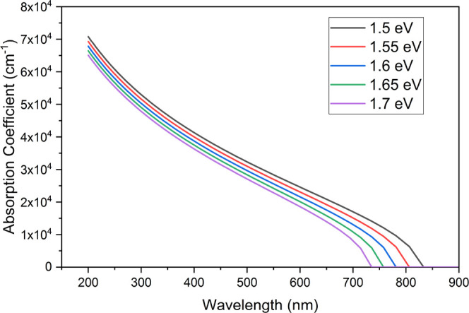
Optical absorption coefficient of Cs-based perovskite materials.
The parameters’ ranges of the perovskite layer were chosen based on published data for Cs-based perovskites reported and validated through both computational and theoretical methods.41,44,45,50−56 These data have been consolidated in Table 1.
Table 2 shows the modulation range, increment δ, and the total number of steps for all of these input material parameters. All possible combinations of the input parameters were utilized to generate 63,500 unique devices, and their outputs including the key parameters defined in Section 2.1, Voc, Jsc, FF, and η, are provided in the Supporting Document. For the ML model and decision-making algorithm, the present research focused solely on the value of device PCE (η), which, as shown previously in Section 2.1, is a function of the Voc, Jsc, and FF.
Table 2. Perovskite Layer Parameters’ Range with Increments and Steps.
| parameter (with units) | range | increment delta | total number of steps |
|---|---|---|---|
| relative permittivity (εr) | 7–11 | 1 | 5 |
| bandgap energy (eV) | 1.5–1.7 | 0.05 | 5 |
| electron affinity (eV) | 4.15–4.30 | 0.05 | 4 |
| electron mobility (cm2/V.s) | 20–100 | 20 | 5 |
| hole mobility (cm2/V.s) | 20–100 | 20 | 5 |
| conduction band DoS (Nc) (cm–3) | 2 × 10¹⁸–1 × 10¹⁹ | 2 × 10¹⁸ | 5 |
| valence band DoS (Nv) (cm–3) | 2 × 10¹⁸–1 × 10¹⁹ | 2 × 10¹⁸ | 5 |
A holistic breakdown of the input parameters of the three layers (ETL, absorber, HTL) as needed by SCAPS has been provided in Table 3. As can be seen, all parameters for the ETL and HTL are held static, together with a few of the Cs-based perovskite absorber parameters (thickness, donor concentration, acceptor concentration, radiative recombination) for ensuring focus on the more important parameters (explained below). The values were thoroughly extracted from previously published experiments and simulation-based literature,41,44,45,57−65 with experimental findings validated against computational values.
It is important to reiterate the perspective and context for the present research here. While the ETL and HTL layers impact the overall performance of the device, the main focus of present research is to probe the nontoxic absorber layer, where the most important photovoltaic actions of light capture, exciton generation, charge transport, and recombination occur. The given seven parameters (relative permittivity, bandgap energy, electron affinity, electron mobility, hole mobility, conduction band DoS, valence band DoS) were chosen to be varied due to the direct way they can be experimentally probed and changed by varying material synthesis, deposition, and overall device fabrication conditions. At the end of the day, the goal of this ML project is to provide incisive insights into input materials’ parameter impact on final device efficiency, with an ability to rank these impacts. This guidance can assist experimentalists directly in making high-efficiency devices.
2.4. Machine Learning Workflow
Data wrangling is a necessary step for a purely experimental dataset.66 There can potentially be multiple measurements and different outputs for the same processing input parameter values in experimental settings. There is a need therefore to clean the data, based on experimental reliability and other factors. For the present research, the entire dataset was generated through simulation utilizing SCAPS-1D software. Again, a Decision Tree model was utilized for the current research; data preprocessing was therefore not required since tree-based models can handle qualitative predictors, i.e., they can generate predictions.67 By contrast, data normalization and some other preprocessing steps are required in other models. Therefore, the raw output data from SCAPS, without any special data processing, was fully utilized.
The raw imported data was a combination of the independent input parameters as listed in Table 1 (also known in the Data Science field as ‘features’) and the solar device outputs (which are the dependent variables and also called ‘target variables’). This initial data was split into two single datasets: one containing the features and the other containing the target variables.
After splitting the raw data into features and targets, 75% of the dataset (the raw Data) was utilized to train the model, and the rest (25%) was used as the test set; the test set remained unseen, that is, independent from the model, during its execution for predicting the output.
We employed a decision tree model, which is one of the most used machine learning models due to its ease of understanding and clarity.68 Even though the model’s outcomes are discrete and appear as clustered data, it is easy to grasp and analyze,69 and it allows the finding of the most important features and correlations among multiple parameters using an intuitive method. As a result, the model provides extremely precise forecasts.70 The model was trained using the RandomForestRegressor class71 from scikit-learn (a highly useful library for ML used for classification, regression, clustering, etc.). As decision tree is identical to random forest having only one tree,72 the hyperparameter (which regulates the learning), namely, ‘n estimators’, was chosen to the default value 1. So, the significance of using random forest decision tree model is that when overfitting is suspected to occur in a decision tree, it may be possible to tune the hyperparameter ‘n estimators’, that represents the number of trees. Overfitting is suspected if the model performs excellently on the training set but performs badly on the test dataset, i.e., the test accuracy is significantly lower.73
After generating output data utilizing SCAPS, the decision tree model was utilized to fit the dataset; after evaluating its performance, features were generated and ranked relative to each other. The decision tree was visualized by taking only the most impactful parameters, together with generating a prediction toward how to tune the parameters for attaining higher device PCE values. The relative importance of features can also be known from the correlation matrix74 by creating a correlation between the features and the target variable. Feature importance75,76 in random forest provides a similar outcome as a correlation matrix does but can rank the input parameters as a function of importance based on impact on the output, provided that the model performs well.
Upon executing the random forest model, the less important features in impacting the device PCE (valence band density of state, conduction band density of state, electron mobility, and permittivity) were excluded, and a new data utilizing only the most important features was created. This new data had the same number of rows compared to the initial data, but the features (input parameters) were no longer unique, i.e., there were multiple outputs with the same sets of features (Table 4). Among the total 63,500 rows in the data, only 100 rows of features were found to be unique. At this junction, the lowest of the different efficiency (PCE) values from the rows with similar feature sets were accepted in the data, thereby ensuring that at least that device PCE may be produced for a specific set of input parameters. This decision helped illustrate the model and paves the way to modify the input settings to increase the ultimate device efficiency.
Table 4. New Data after Excluding the Four Least Important Input Material Parameter Columns.
| EA (eV) | Eg (eV) | h mobility (cm2/V.s) | PCE (%) | |
|---|---|---|---|---|
| 0 | 4.15 | 1.5 | 20 | 11.7929 |
| 1 | 4.15 | 1.5 | 20 | 11.7865 |
| 2 | 4.15 | 1.5 | 20 | 11.7802 |
| 3 | 4.15 | 1.5 | 20 | 11.7739 |
| 4 | 4.15 | 1.5 | 20 | 11.7677 |
| ... | ... | ... | ... | ... |
| 63,495 | 4.3 | 1.7 | 100 | 9.1986 |
| 63,496 | 4.30 | 1.7 | 100 | 9.2009 |
| 63,497 | 4.30 | 1.7 | 100 | 9.2031 |
| 63,498 | 4.30 | 1.7 | 100 | 9.2051 |
| 63,499 | 4.30 | 1.7 | 100 | 9.2070 |
The Supporting Documentation includes the Python code (in a Jupyter notebook) used to analyze the data for the present study.
3. Results and Discussion
In this investigation, we utilized the solar cell simulation dataset and machine learning models to delineate the relative impacts of materials’ intrinsic parameters on the overall power conversion efficiency. It is known that various parameters are innately responsible for impacting the efficiency of solar devices; this theoretical study was focused on concentrating on those parameters that are more impactful on the device efficiency over others.
3.1. Evaluating Decision Tree Model Performance
Evaluating prediction accuracies for both training and testing datasets as well as other error metrics (different performance analyzing metrics used in statistics, e.g., RMSE, R2) were utilized to assess the model’s performance. The initial test and train datasets were calculated through the SCAPS-1D software. Both datasets are based on the computational framework that utilizes intrinsic device input parameters such as bandgap, electron affinity, conduction band density of state, valence band density of state, intrinsic defect density, acceptor density, etc. to provide device scale photovoltaic output parameters such as open-circuit voltage (Voc), closed-circuit current (Jsc), fill factor (FF), and power conversion efficiency (PCE). For the modeled dataset in this investigation, PCE is considered the target value as it depicts an accurate representation of the overall output device performance. SCAPS-1D simulation software is based upon a rigid computational framework. Relative importance and correlation between the intrinsic parameters were analyzed through supervised machine learning algorithms. Both the train and test sets show high accuracy. This is validated by evaluating the error metrics. Figure 5 shows the parity plot for training data and test data side by side, indicating that the model predicts both the train and test datasets with high levels of accuracy.
Figure 5.

Parity plot for train and test data side by side.
The below statistical metrics numerically validate this observation
However, to get an unbiased estimate of accuracy, RepeatedKFold cross-validation from scikit-learn77 was used. In the k-fold cross-validation process, a restricted dataset is divided into k nonoverlapping folds. The technique can be replicated numerous times using repeated k-fold cross-validation. The cross-validation relied on the test train dataset and was not compared or contrasted with any experimental data or input from any other source. If five-fold cross-validation was conducted 5 times, the model’s effectiveness would be estimated using 25 distinct sets. In the current research, while the dataset was split once for the single train and test validation, it was now split 5 times and the train and test sequences were repeated 5 times. The process was executed randomly, i.e., without any bias. As before, the standard error metrics including RMSE, R2, were repeated for the k-fold cross-validation.
As before, as can be seen, the model generated high levels of accuracy in its prediction for both train and test datasets.
These high accuracy numbers for the train and test datasets are likely a function of overfitting, indicating the possibility of some similar devices in the dataset. Looking closer, the 63,500 devices are stepwise cartesian products of seven parameters, i.e., a combination of different input parameter sets, as discussed in Table 2. It is therefore possible that certain parameters are not important and do not influence the output parameter. By excluding the least important features, which have little or no influence on device efficiency, only some of the rows will be unique among the 63,500 rows. In the subsequent analysis, we used the unique devices after dropping the least important features.
3.2. Generating a Prediction
With high confidence generated from cross-validation of the model in the previous section, the model was then utilized to predict the most important features, i.e., those which have the highest impact on the target. To this end, two different analyses built into the random forest algorithm, Feature Importance and Shapley Additive exPlanations (SHAP) analysis, were utilized.
3.2.1. Feature Relative Importance
The random forest model75,76 from the scikit-learn package is used to calculate feature relative importance. There are one or more decision trees in a random forest model, and each decision tree is made up of internal nodes and leaves. The choice is done at the internal nodes by selecting a feature (valence and conduction band density of state, electron affinity, bandgap, electron mobility, hole mobility, or permittivity) and then splitting the data into two separate sets. It calculates how much each attribute reduces the “impurity” of the split (the feature with the greatest reduction is chosen for the internal node). For random forest regression, variance reduction is the measurement of the decrease in impurity (reduction in variance between two sample sets, i.e., difference between variance of a node and weighted sum of variances of its child nodes). The methodology calculates that for each feature variance is decreased on average. The average overall trees are the measurement of feature importance in random forest. These results are listed in Table 5 and graphically demonstrated in Figure 6.
Table 5. Parameters and Their Relative Importance.
| parameter/absorber layer | relative importance (%) |
|---|---|
| bandgap energy | 77.40 |
| hole mobility | 10.32 |
| electron affinity | 9.70 |
| valence band DoS | 1.31 |
| conduction band DoS | 1.26 |
| relative permittivity | 0.01 |
| electron mobility | 0.00 |
Figure 6.

Relative strengths of importance indices of features.
Additional validation was done utilizing the correlation matrix. The correlation of the features with the target variable showcased the same result, as seen in Table 6.
Table 6. Correlation of Features with the Target.
| features (input material parameters) | correlation |
|---|---|
| bandgap energy | 0.868535 |
| hole mobility | 0.302746 |
| electron affinity | 0.149510 |
| conduction band DoS | 0.104182 |
| valence band DoS | 0.068954 |
| electron mobility | 0.000688 |
| relative permittivity | 0.000307 |
The correlation matrix showcases the high feature importance of bandgap energy among the seven features. The features reported here act as input parameters for the SCAPS-1D simulation software; Table 6 showcases the impact of these features on the simulated device PCE (target). The outcome from this exercise provides clarity as to which features to modulate to ultimately impact the PCE of the simulated device.
3.2.2. Shapley Additive exPlanations (SHAP) Analysis
To determine the ultimate importance forecast of features the model generates, a SHAP analysis has also been performed on that model. The package Shapley Additive exPlanations (SHAP) is a package of methods most often used for prediction; focusing on the relative importance of features provides a measurement of which variables have the most effect in the model. SHAP analysis creates a large number of predictions and evaluates the results through a comparative review. SHAP combines feature significance and impact in a summary plot. The SHAP summary plot showing the relative importance of noncorrelated features (in descending order) on efficiency is illustrated in Figure 7.
Figure 7.

Noncorrelated features’ contribution on device PCE as measured by SHAP with random forest regression (in decreasing order).
Overall, it is observed through utilizing both methods that the three most important features, bandgap, hole mobility, and electron affinity (highest to lowest), have more than 97% impact on the target variable (device PCE). This information and insight are critical for the experimentalists, in particular, to enable them to effectively focus their efforts on the optimization of these parameters over the others in their efforts to improve device power conversion efficiency.
3.3. Visualizing the Decision Tree
Many ML models are “black boxes”; their inner workings are not interpretable to humans. Decision trees are often chosen because they are more explainable than other models. Here, Boolean logic can simply explain the circumstances, making it easier to understand in comparison to a black box model (such as an artificial neural network).69 So, after a concise overview, most users can comprehend decision tree models. Trees can also be visually represented in a form that is simple to understand for nonexperts.67 Implication of the decision tree model to similar systems can be found in research papers.78,79 To provide clarity, a visualization of the decision tree model utilized in this current research has been shown in Figure 8.
Figure 8.

Branch of the decision tree with only pure leaf nodes, demonstrating a route to achieve higher PCE.
From Figure 8, it can be visualized that for increasing PCE bandgap energy, X2 < 1.625, X2 < 1.575 & X2 < 1.525, i.e., bandgap energy, X2 < 1.525 eV; hole mobility, X1 > 30, X1 > 50, X1 > 70 & X1 > 90, i.e., hole mobility, X1 > 90 cm2/V.s; and electron affinity, X0 > 4.175, X0 > 4.225 & X0 < 4.275, i.e., electron affinity, 4.225 < X0 < 4.275 eV.
In the given dataset, corresponding bandgap, hole mobility, and EA for maximum device PCE (13.2912%) are 1.5 eV, 100 cm2/V.s, and 4.25 eV, respectively. From the decision tree, it can be visualized that PCE decreases as the value of bandgap energy (X2) increases and hole mobility (X1) decreases. It is additionally observed that PCE decreases with either an increase or decrease in EA (X0) from the approximate critical value of 4.25 eV while holding other parameters unchanged. This behavior indicates that EA should be optimized to be a value near 4.25 eV in practice. However as decision tree predictions are piecewise constant approximations, rather than continuous predictions, it is challenging to extrapolate them.80 This indicates that a numerical value higher than the maximum value of a given output cannot be predicted. The output value beyond the maximum point loses any physical meaning. If the parameters are modulated any other way, the output value starts decreasing. For the present research and with the generated datasets, these observations, therefore, indicate that the device PCE increases as the bandgap energy decreases from 1.5 eV and the hole mobility increases from 100 eV. The inequality for each parameter sets the PCE that the solar device can produce and is tabulated in Table 7.
Table 7. Most Impactful Parameters and Their Inequalities for Increasing Device PCE.
| parameter/absorber Layer | inequality for increasing efficiency |
|---|---|
| bandgap energy (eV) | ≤1.5 |
| hole mobility (cm2/V.s) | ≥100 |
| electron affinity (eV) | ≈4.25 |
The above conditions are ‘AND’ conditions. So, bandgap energy has to be <1.5 eV AND hole mobility has to be >100 cm2/V.s AND electron affinity is static at approximately 4.25 eV.
The three-dimensional (3-D) representation in Figure 9 and the contour plot (a graphical representation of a 3-D surface in a two-dimensional (2-D) format by drawing constant z slices) in Figure 10 both show that the device PCE increases with decreasing bandgap energy and increasing the hole mobility. These representations additionally suggest that device PCE is maximum at an EA value of 4.25 eV.
Figure 9.
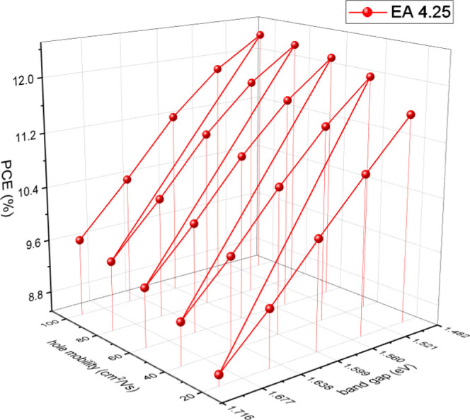
PCE as a function of changing bandgap and hole mobility, and at a constant EA 4.25 eV.
Figure 10.

Contour plots showing the relation of bandgap and hole mobility with device PCE at different EA values (A) 4.15, (B) 4.20, (C) 4.25, and (D) 4.30 eV.
4. Device Optimization through SCAPS-1D
Supervised machine learning on the selective devices in the earlier discussion (Section 3) provided a set of critical intrinsic material parameters for a champion device. As indicated from the target analysis, the parameters for that particular device are likely to yield excellent photovoltaic performance. Further optimizations of absorber layer thickness, back contact metal work function, and bulk defect density can significantly impact the device performance. In this section, step-by-step optimizations have been conducted through SCAPS-1D simulation software. An additional set of critical analyses including interfacial defect and device stability showcases the experimental viability of the champion device. The modulations and PCE values that have been calculated to facilitate this investigation are purely based on computational modeling. The calculations highlighted in this section have been carried out through the SCAPS-1D simulation software. The intuition generated from these calculations to improve device performance can ultimately be applied to experimental settings.
4.1. Bulk Absorber Layer Thickness Optimization
Inorganic and organic perovskite devices are fabricated through various deposition methods. In most cases, high bulk layer thickness leads to the high absorption of solar energy. But after a certain thickness, most perovskites become susceptible to intrinsic and extrinsic defects. For this section, absorber layer thickness was varied from 0.3 to 1.6 μm. The results illustrated in Figure 11 indicate that peak PCE of 16.68% occurs at 1 μm perovskite layer thickness. For this particular device, therefore, it can be concluded that the highest PCE value of 16.68% can be obtained for the absorber thickness of 1 μm provided there are no additional defects in the bulk of the absorber. The overall trends indicate that Voc and FF decrease with increasing absorber layer thickness owing to the proportionate increase of defect sites within the film. Since a bulkier absorber generates more electron–hole pairs, Jsc rises with absorber layer thickness, resulting in a higher photocurrent.
Figure 11.

J–V characteristic parameters as a function of absorber (perovskite) thickness: (a) Voc, (b) Jsc, (c) FF, and (d) PCE.
4.2. Bulk and Interfacial Defect Investigation
The bulk defect is a critical cause of low performance for most organic and inorganic Sn-based devices. In atmospheric conditions, Sn-based perovskites have the tendency to be oxidized to Sn2+, which compromises the photovoltaic energy conversion. Although defect level densities are highly dependent on experimental process routes, device performance at different defect energy and defect concentration can provide a comparative study that can be utilized for optimizing experimental conditions. The results of solar output parameters as a function of defect level and energy are illustrated in Figure 12.
Figure 12.

Characteristic device parameters: (a) Voc, (b) Jsc, (c) FF, and (d) PCE at different defect concentrations and energy levels for the bulk absorber layer.
From the data, it is apparent that higher defect concentration may decrease the device performance significantly. Lowering the defect to 1 × 1014 cm–3 can yield up to a 40% increase in the device performance. However, such a low defect concentration is yet to be practical with the commercial thin film deposition route and a realistic 1 × 1016 cm–3 concentration of defect is considered for this investigation.
Defect concentration in the interfaces can severely impact the device performances as well. In Figures 13 and 14, defect concentrations at the HTL/absorber and ETL/absorber interfaces were investigated. From the outputs, it can be seen that higher defect concentrations at the HTL/absorber interface lower the device performance more severely than defects at the ETL/absorber interface.
Figure 13.

Characteristic parameters: (a) Voc, (b) Jsc, (c) FF, and (d) PCE at different defect concentrations and energy levels for the HTL/absorber interface.
Figure 14.

Characteristic parameters: (a) Voc, (b) Jsc, (c) FF, and (d) PCE at different defect concentrations and energy levels for the ETL/absorber interface.
The results of the bulk and interfacial defect analyses also clarify the influence of various defects on overall device performance. For instance, in the device bulk layer, defects with energies ranging from 0.3 to 1.4 eV may be categorized as deep defects, which have a significant negative influence on the device’s performance and should be avoided as far as possible. In contrast, at the interfaces between the absorber and the HTL, defects between the energy level of 0 and 1.1 eV can be classified as deep defects. It can be concluded that the severity of the defects in the photovoltaic performance is also subjective and dependent on the position, concentration, and energy level of the subsequent defect.
4.3. Choice of Back Contact Metals
Perovskite solar devices are in general integrated into the circuit board through the soldering of precious metals like silver and gold. The selection of the material can provide a better engineering and economic choice for the design of the subsequent devices. For the device simulation, the metal work function (which is the characteristic indicative parameter for every subsequent back contact metal) has been varied to analyze its impact on the photovoltaic performance.
From the results showcased in Figure 15, it is apparent that back contact metals with their corresponding work function values of above 4.9 eV will yield relatively consistent device performance. Popular back contact metals like silver yield a lower work function of 4.6 eV and thereby should be considered a poor choice for this device.44,81
Figure 15.

Characteristic parameters: (a) Voc, (b) Jsc, (c) FF, and (d) PCE utilizing different back contact metal work functions.
4.4. Quantum Efficiency and the J–V Curve of the Champion Device
Quantum efficiency for solar devices is a reliable metric that indicates the solar energy absorption potential. For solar devices to absorb high photovoltaic energy from the irradiation of the sun, high quantum efficiency in the region between 1.5 and 3 eV radiation is recommended.82 External quantum efficiency (EQE) as a function of photon energy for the given optimized device (optimized through bulk absorber thickness, defect concentration, and back contact metal) is illustrated in Figure 16. The device demonstrated excellent EQE (85–95%) for the photons within the range of 2–3.5 eV energy. These results highlight the beneficial absorption potential for this discovered device under normal solar irradiation.
Figure 16.
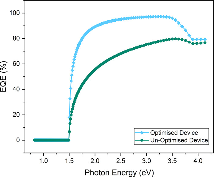
External quantum efficiency (EQE) at different photon energy levels for the champion device before and after optimization.
Characteristic J–V parameter optimizations through step-by-step modulation of absorber layer thickness, defect density, and back contact metal have a remarkable impact on the overall performance of the device, as can be seen from Figure 17. The device PCE of the champion devices of the fully optimized device (16.68%) is significantly higher than that of the unoptimized device 13.29%.
Figure 17.

J–V curve of the optimized and unoptimized devices.
5. Conclusions
An ML exercise was performed on Cs-perovskite-based solar devices, focusing on key input materials with an intent to delineate their impacts on ultimate device PCE. Supervised machine learning was conducted on the simulated parameters of the SCAPS-1D software where the target value was the theoretical photovoltaic efficiency of the device. It was demonstrated that the energy bandgap, hole mobility, and electron affinity of the absorber perovskite were the most impactful parameters, rendering them to be areas of focus and modification to obtain high device PCE. After generating these impactful parameters and excluding the rest, the decision tree for the model was visualized. It was demonstrated that the electron affinity of the perovskite material should be optimized to a specific value while maintaining critical inequality ranges for the bandgap and hole mobility. The combination of these criteria can lead to the realization of improved device PCE. Further improvement on the device performance was conducted through the optimization of several intrinsic parameters like bulk absorber thickness, defect concentration, and back contact metal that remarkably improved the overall PCE of the device from 13.29% (unoptimized) to 16.68% (optimized). It is important to note that the current investigation is theoretical in nature; further clarification can be obtained from experimental data. The insights provided herewith nonetheless should offer experimentalists a keen sense of targeting specific material parameters over others together with validating their impacts on device PCE.
Acknowledgments
S.A. acknowledges the support of the Clean Energy Grant (Project #53) from SUNY Buffalo State.
Supporting Information Available
The Supporting Information is available free of charge at https://pubs.acs.org/doi/10.1021/acsomega.2c01076.
layer-by-layer materials used for the simulation; a step-by-step machine learning workflow for our analysis is included (PDF)
Author Contributions
∇ M.S.I., M.T.I., and S.S. contributed equally to this work.
The authors declare no competing financial interest.
Notes
As the raw and processed data to replicate these findings is part of an ongoing investigation, it cannot be disclosed at this stage.
Supplementary Material
References
- Sarker I. H. Machine Learning: Algorithms, Real-World Applications and Research Directions. SN Comput. Sci. 2021, 2, 160 10.1007/s42979-021-00592-x. [DOI] [PMC free article] [PubMed] [Google Scholar]
- Awad M.; Khanna R.. Machine Learning. In Efficient Learning Machines; Apress: Berkeley, CA, 2015; pp 1–18. [Google Scholar]
- Jordan M. I.; Mitchell T. M. Machine Learning: Trends, Perspectives, and Prospects. Science 2015, 349, 255–260. 10.1126/science.aaa8415. [DOI] [PubMed] [Google Scholar]
- Wei J.; Chu X.; Sun X.; Xu K.; Deng H.; Chen J.; Wei Z.; Lei M. Machine Learning in Materials Science. InfoMat 2019, 1, 338–358. 10.1002/inf2.12028. [DOI] [Google Scholar]
- Wu W.; Sun Q. Applying Machine Learning to Accelerate New Materials Development. Sci. Sin. Phys. Mech. Astron. 2018, 48, 107001 10.1360/sspma2018-00073. [DOI] [Google Scholar]
- Al Jame H.; Sarker S.; Islam M. S.; Islam T. M.; Rauf A.; Ahsan S.; Nishat S. S.; Jani M. R.; Shorowordi K. M.; Carbonara J.; Ahmed S. Supervised Machine Learning-Aided SCAPS-Based Quantitative Analysis for the Discovery of Optimum Bromine Doping in Methylammonium Tin-Based Perovskite (MASnI3–XBrx). ACS Appl. Mater. Interfaces 2022, 14, 502–516. 10.1021/acsami.1c15030. [DOI] [PubMed] [Google Scholar]
- Tao Q.; Xu P.; Li M.; Lu W. Machine Learning for Perovskite Materials Design and Discovery. npj Comput. Mater. 2021, 7, 23 10.1038/s41524-021-00495-8. [DOI] [Google Scholar]
- Sutherland B. R.; Sargent E. H. Perovskite Photonic Sources. Nat. Photonics 2016, 10, 295–302. 10.1038/nphoton.2016.62. [DOI] [Google Scholar]
- Tilley R. J. D.The ABX 3 Perovskite Structure. In Perovskites; John Wiley & Sons, Ltd., 2016; pp 1–41. [Google Scholar]
- Qian J.; Xu B.; Tian W. A Comprehensive Theoretical Study of Halide Perovskites ABX3. Org. Electron. 2016, 37, 61–73. 10.1016/j.orgel.2016.05.046. [DOI] [Google Scholar]
- Grill I.; Aygüler M. F.; Bein T.; Docampo P.; Hartmann N. F.; Handloser M.; Hartschuh A. Charge Transport Limitations in Perovskite Solar Cells: The Effect of Charge Extraction Layers. ACS Appl. Mater. Interfaces 2017, 9, 37655–37661. 10.1021/acsami.7b09567. [DOI] [PubMed] [Google Scholar]
- Shi M.; Li R.; Li C. Halide Perovskites for Light Emission and Artificial Photosynthesis: Opportunities, Challenges, and Perspectives. EcoMat 2021, 3, e12074 10.1002/eom2.12074. [DOI] [Google Scholar]
- Elseman A. M.; Sharmoukh W.; Sajid S.; Cui P.; Ji J.; Dou S.; Wei D.; Huang H.; Xi W.; Chu L.; Li Y.; Jiang B.; Li M. Superior Stability and Efficiency Over 20% Perovskite Solar Cells Achieved by a Novel Molecularly Engineered Rutin–AgNPs/Thiophene Copolymer. Adv. Sci. 2018, 5, 1800568 10.1002/advs.201800568. [DOI] [PMC free article] [PubMed] [Google Scholar]
- Cui P.; Wei D.; Ji J.; Song D.; Li Y.; Liu X.; Huang J.; Wang T.; You J.; Li M. Highly Efficient Electron-Selective Layer Free Perovskite Solar Cells by Constructing Effective p–n Heterojunction. Sol. RRL 2017, 1, 1600027 10.1002/solr.201600027. [DOI] [Google Scholar]
- Kojima A.; Teshima K.; Shirai Y.; Miyasaka T. Organometal Halide Perovskites as Visible-Light Sensitizers for Photovoltaic Cells. J. Am. Chem. Soc. 2009, 131, 6050–6051. 10.1021/ja809598r. [DOI] [PubMed] [Google Scholar]
- Li Z.; Zhao Y.; Wang X.; Sun Y.; Zhao Z.; Li Y.; Zhou H.; Chen Q. Cost Analysis of Perovskite Tandem Photovoltaics. Joule 2018, 2, 1559–1572. 10.1016/j.joule.2018.05.001. [DOI] [Google Scholar]
- Jaishankar M.; Tseten T.; Anbalagan N.; Mathew B. B.; Beeregowda K. N. Toxicity, Mechanism and Health Effects of Some Heavy Metals. Interdiscip. Toxicol. 2014, 60–72. 10.2478/intox-2014-0009. [DOI] [PMC free article] [PubMed] [Google Scholar]
- Babayigit A.; Thanh D. D.; Ethirajan A.; Manca J.; Muller M.; Boyen H. G.; Conings B. Assessing the Toxicity of Pb-and Sn-Based Perovskite Solar Cells in Model Organism Danio Rerio. Sci. Rep. 2016, 6, 18721 10.1038/srep18721. [DOI] [PMC free article] [PubMed] [Google Scholar]
- Sall M. L.; Diaw A. K. D.; Gningue-Sall D.; Aaron S. E.; Aaron J. J. Toxic Heavy Metals: Impact on the Environment and Human Health, and Treatment with Conducting Organic Polymers, a Review. Environ. Sci. Pollut. Res. 2020, 27, 29927–29942. 10.1007/s11356-020-09354-3. [DOI] [PubMed] [Google Scholar]
- Su P.; Liu Y.; Zhang J.; Chen C.; Yang B.; Zhang C.; Zhao X. Pb-Based Perovskite Solar Cells and the Underlying Pollution behind Clean Energy: Dynamic Leaching of Toxic Substances from Discarded Perovskite Solar Cells. J. Phys. Chem. Lett. 2020, 11, 2812–2817. 10.1021/acs.jpclett.0c00503. [DOI] [PubMed] [Google Scholar]
- Jokar E.; Chien C. H.; Fathi A.; Rameez M.; Chang Y. H.; Diau E. W. G. Slow Surface Passivation and Crystal Relaxation with Additives to Improve Device Performance and Durability for Tin-Based Perovskite Solar Cells. Energy Environ. Sci. 2018, 11, 2353–2362. 10.1039/C8EE00956B. [DOI] [Google Scholar]
- Ju M. G.; Chen M.; Zhou Y.; Dai J.; Ma L.; Padture N. P.; Zeng X. C. Toward Eco-Friendly and Stable Perovskite Materials for Photovoltaics. Joule 2018, 2, 1231–1241. 10.1016/j.joule.2018.04.026. [DOI] [Google Scholar]
- Wang M.; Wang W.; Ma B.; Shen W.; Liu L.; Cao K.; Chen S.; Huang W. Lead-Free Perovskite Materials for Solar Cells. Nano-Micro Lett. 2021, 62 10.1007/s40820-020-00578-z. [DOI] [PMC free article] [PubMed] [Google Scholar]
- Abate A. Perovskite Solar Cells Go Lead Free. Joule 2017, 659–664. 10.1016/j.joule.2017.09.007. [DOI] [Google Scholar]
- Ke W.; Kanatzidis M. G. Prospects for Low-Toxicity Lead-Free Perovskite Solar Cells. Nat. Commun. 2019, 965 10.1038/s41467-019-08918-3. [DOI] [PMC free article] [PubMed] [Google Scholar]
- Li J.; Duan J.; Yang X.; Duan Y.; Yang P.; Tang Q. Review on Recent Progress of Lead-Free Halide Perovskites in Optoelectronic Applications. Nano Energy 2021, 80, 105526 10.1016/j.nanoen.2020.105526. [DOI] [Google Scholar]
- Bella F.; Renzi P.; Cavallo C.; Gerbaldi C. Caesium for Perovskite Solar Cells: An Overview. Chem. - Eur. J. 2018, 24, 12183–12205. 10.1002/chem.201801096. [DOI] [PubMed] [Google Scholar]
- Burgelman M.; Nollet P.; Degrave S. Modelling Polycrystalline Semiconductor Solar Cells. Thin Solid Films 2000, 361–362, 527–532. 10.1016/S0040-6090(99)00825-1. [DOI] [Google Scholar]
- Decock K.; Zabierowski P.; Burgelman M. Modeling Metastabilities in Chalcopyrite-Based Thin Film Solar Cells. J. Appl. Phys. 2012, 111, 043703 10.1063/1.3686651. [DOI] [Google Scholar]
- Islam M. T.; Jani M. R.; Al Amin S. M.; Sami M. S. U.; Shorowordi K. M.; Hossain M. I.; Devgun M.; Chowdhury S.; Banerje S.; Ahmed S. Numerical Simulation Studies of a Fully Inorganic Cs2AgBiBr6 Perovskite Solar Device. Opt. Mater. 2020, 105, 109957 10.1016/j.optmat.2020.109957. [DOI] [Google Scholar]
- Islam M. T.; Jani M. R.; Rahman S.; Shorowordi K. M.; Nishat S. S.; Hodges D.; Banerjee S.; Efstathiadis H.; Carbonara J.; Ahmed S. Investigation of Non-Pb All-Perovskite 4-T Mechanically Stacked and 2-T Monolithic Tandem Solar Devices Utilizing SCAPS Simulation. SN Appl. Sci. 2021, 3, 504 10.1007/s42452-021-04487-7. [DOI] [Google Scholar]
- Rahman M. A. Design and Simulation of a High-Performance Cd-Free Cu2SnSe3 Solar Cells with SnS Electron-Blocking Hole Transport Layer and TiO2 Electron Transport Layer by SCAPS-1D. SN Appl. Sci. 2021, 3, 253 10.1007/s42452-021-04267-3. [DOI] [Google Scholar]
- Sze S. M.; Ng K. K.. Physics of Semiconductor Devices; John Wiley & Sons, Inc., 2006. [Google Scholar]
- Kartikay P.; Mokurala K.; Sharma B.; Kali R.; Mukurala N.; Mishra D.; Kumar A.; Mallick S.; Song J.; Jin S. H. Recent Advances and Challenges in Solar Photovoltaic and Energy Storage Materials: Future Directions in Indian Perspective. J. Phys.: Energy 2021, 3, 034018 10.1088/2515-7655/AC1204. [DOI] [Google Scholar]
- Zhou D.; Zhou T.; Tian Y.; Zhu X.; Tu Y. Perovskite-Based Solar Cells: Materials, Methods, and Future Perspectives. J. Nanomater. 2018, 2018, 1–15. 10.1155/2018/8148072. [DOI] [Google Scholar]
- Edri E.; Kirmayer S.; Cahen D.; Hodes G. High Open-Circuit Voltage Solar Cells Based on Organic-Inorganic Lead Bromide Perovskite. J. Phys. Chem. Lett. 2013, 4, 897–902. 10.1021/jz400348q. [DOI] [PubMed] [Google Scholar]
- Im J. H.; Lee C. R.; Lee J. W.; Park S. W.; Park N. G. 6.5% Efficient Perovskite Quantum-Dot-Sensitized Solar Cell. Nanoscale 2011, 3, 4088–4093. 10.1039/c1nr10867k. [DOI] [PubMed] [Google Scholar]
- Kaminski P. M.; Isherwood P. J. M.; Womack G.; Walls J. M. Optical Optimization of Perovskite Solar Cell Structure for Maximum Current Collection. Energy Procedia 2016, 102, 11–18. 10.1016/j.egypro.2016.11.312. [DOI] [Google Scholar]
- Lee K. M.; Lin W. J.; Chen S. H.; Wu M. C. Control of TiO2 Electron Transport Layer Properties to Enhance Perovskite Photovoltaics Performance and Stability. Org. Electron. 2020, 77, 105406 10.1016/j.orgel.2019.105406. [DOI] [Google Scholar]
- Kanoun M. B.; Kanoun A. A.; Merad A. E.; Goumri-Said S. Device Design Optimization with Interface Engineering for Highly Efficient Mixed Cations and Halides Perovskite Solar Cells. Results Phys. 2021, 20, 103707 10.1016/j.rinp.2020.103707. [DOI] [Google Scholar]
- Islam M. T.; Jani M. R.; Islam A. F.; Shorowordi K. M.; Chowdhury S.; Nishat S. S.; Ahmed S. Investigation of CsSn0.5Ge0.5I3-on-Si Tandem Solar Device Utilizing SCAPS Simulation. IEEE Trans. Electron Devices 2021, 68, 618–625. 10.1109/TED.2020.3045383. [DOI] [Google Scholar]
- Fonash S. J.Material Properties and Device Physics Basic to Photovoltaics. In Solar Cell Device Physics; Elsevier, 2010; pp 9–65. [Google Scholar]
- Crovetto A.; Huss-Hansen M. K.; Hansen O. How the Relative Permittivity of Solar Cell Materials Influences Solar Cell Performance. Sol. Energy 2017, 149, 145–150. 10.1016/j.solener.2017.04.018. [DOI] [Google Scholar]
- Jani M. R.; Islam M. T.; Al Amin S. M.; Sami M. S. U.; Shorowordi K. M.; Hossain M. I.; Chowdhury S.; Nishat S. S.; Ahmed S. Exploring Solar Cell Performance of Inorganic Cs2TiBr6 Halide Double Perovskite: A Numerical Study. Superlattices Microstruct. 2020, 146, 106652 10.1016/j.spmi.2020.106652. [DOI] [Google Scholar]
- Islam M. T.; Jani M. R.; Shorowordi K. M.; Hoque Z.; Gokcek A. M.; Vattipally V.; Nishat S. S.; Ahmed S. Numerical Simulation Studies of Cs3Bi2I9 Perovskite Solar Device with Optimal Selection of Electron and Hole Transport Layers. Optik 2021, 231, 166417 10.1016/j.ijleo.2021.166417. [DOI] [Google Scholar]
- Gfroerer T. H.; Wanlass M. W. In IEEE 4th World Conference on Photovoltaic Energy Conference, Recombination in Low-Bandgap InGaAs, 2006; pp 780–782.
- Gfroerer T. H.; Priestley L. P.; Falrley M. F.; Wanlass M. W. Temperature Dependence of Nonradiative Recombination in Low-Band Gap InxGa1–xAs/InAsyP1–y Double Heterostructures Grown on InP Substrates. J. Appl. Phys. 2003, 94, 1738–1743. 10.1063/1.1586468. [DOI] [Google Scholar]
- McAllister A.; Bayerl D.; Kioupakis E. Radiative and Auger Recombination Processes in Indium Nitride. Appl. Phys. Lett. 2018, 112, 251108 10.1063/1.5038106. [DOI] [Google Scholar]
- Rosencher E.; Vinter B.. Optical Properties of Semiconductors. In Optoelectronics; Cambridge University Press, 2002; pp 296–320. [Google Scholar]
- Qiu X.; Cao B.; Yuan S.; Chen X.; Qiu Z.; Jiang Y.; Ye Q.; Wang H.; Zeng H.; Liu J.; Kanatzidis M. G. From Unstable CsSnI3 to Air-Stable Cs2SnI6: A Lead-Free Perovskite Solar Cell Light Absorber with Bandgap of 1.48 EV and High Absorption Coefficient. Sol. Energy Mater. Sol. Cells 2017, 159, 227–234. 10.1016/j.solmat.2016.09.022. [DOI] [Google Scholar]
- Bai F.; Hu Y.; Hu Y.; Qiu T.; Miao X.; Zhang S. Lead-Free, Air-Stable Ultrathin Cs3Bi2I9 Perovskite Nanosheets for Solar Cells. Sol. Energy Mater. Sol. Cells 2018, 184, 15–21. 10.1016/j.solmat.2018.04.032. [DOI] [Google Scholar]
- Wu C.; Zhang Q.; Liu Y.; Luo W.; Guo X.; Huang Z.; Ting H.; Sun W.; Zhong X.; Wei S.; Wang S.; Chen Z.; Xiao L. The Dawn of Lead-Free Perovskite Solar Cell: Highly Stable Double Perovskite Cs2AgBiBr6 Film. Adv. Sci. 2018, 5, 1700759 10.1002/advs.201700759. [DOI] [PMC free article] [PubMed] [Google Scholar]
- Ming W.; Shi H.; Du M. H. Large Dielectric Constant, High Acceptor Density, and Deep Electron Traps in Perovskite Solar Cell Material CsGeI3. J. Mater. Chem. A 2016, 4, 13852–13858. 10.1039/c6ta04685a. [DOI] [Google Scholar]
- Saparov B.; Hong F.; Sun J. P.; Duan H. S.; Meng W.; Cameron S.; Hill I. G.; Yan Y.; Mitzi D. B. Thin-Film Preparation and Characterization of Cs3Sb2I9: A Lead-Free Layered Perovskite Semiconductor. Chem. Mater. 2015, 27, 5622–5632. 10.1021/acs.chemmater.5b01989. [DOI] [Google Scholar]
- Ahmed S.; Jannat F.; Khan M. A. K.; Alim M. A. Numerical Development of Eco-Friendly Cs2TiBr6 Based Perovskite Solar Cell with All-Inorganic Charge Transport Materials via SCAPS-1D. Optik 2021, 225, 165765 10.1016/j.ijleo.2020.165765. [DOI] [Google Scholar]
- Islam T.; Jani R.; Al Amin S. M.; Shorowordi K. M.; Nishat S. S.; Kabir A.; Taufique M. F. N.; Chowdhury S.; Banerjee S.; Ahmed S. Simulation Studies to Quantify the Impacts of Point Defects: An Investigation of Cs2AgBiBr6 Perovskite Solar Devices Utilizing ZnO and Cu2O as the Charge Transport Layers. Comput. Mater. Sci. 2020, 184, 109865 10.1016/j.commatsci.2020.109865. [DOI] [Google Scholar]
- Gokmen T.; Gunawan O.; Mitzi D. B. Semi-Empirical Device Model for Cu2ZnSn(S,Se)4 Solar Cells. Appl. Phys. Lett. 2014, 105, 033903 10.1063/1.4890844. [DOI] [Google Scholar]
- Lee Y. S.; Heo J.; Winkler M. T.; Siah S. C.; Kim S. B.; Gordon R. G.; Buonassisi T. Nitrogen-Doped Cuprous Oxide as a p-Type Hole-Transporting Layer in Thin-Film Solar Cells. J. Mater. Chem. A 2013, 1, 15416–15422. 10.1039/c3ta13208k. [DOI] [Google Scholar]
- Wang N.; Zhou Y.; Ju M. G.; Garces H. F.; Ding T.; Pang S.; Zeng X. C.; Padture N. P.; Sun X. W. Heterojunction-Depleted Lead-Free Perovskite Solar Cells with Coarse-Grained B-γ-CsSnI3 Thin Films. Adv. Energy Mater. 2016, 6, 1601130 10.1002/aenm.201601130. [DOI] [Google Scholar]
- Du H. J.; Wang W. C.; Zhu J. Z. Device Simulation of Lead-Free CH3NH3SnI3 Perovskite Solar Cells with High Efficiency. Chin. Phys. B 2016, 25, 108802 10.1088/1674-1056/25/10/108802. [DOI] [Google Scholar]
- Delibasis K. K.; Tassani S.; Asvestas P.; Kechriniotis A. I.; Matsopoulos G. K. A Fourier-Based Implicit Evolution Scheme for Active Surfaces, for Object Segmentation in Volumetric Images. Meas. Sci. Technol. 2013, 24, 074021 10.1088/0957-0233/24/7/074021. [DOI] [Google Scholar]
- Zhu L.; Shao G.; Luo J. K. Numerical Study of Metal Oxide Heterojunction Solar Cells. Semicond. Sci. Technol. 2011, 26, 085026 10.1088/0268-1242/26/8/085026. [DOI] [Google Scholar]
- Stamate M. D. On the Dielectric Properties of Dc Magnetron TiO 2 Thin Films. Appl. Surf. Sci. 2003, 218, 318–323. 10.1016/S0169-4332(03)00624-X. [DOI] [Google Scholar]
- Paul G. K.; Nawa Y.; Sato H.; Sakurai T.; Akimoto K. Defects in Cu2 O Studied by Deep Level Transient Spectroscopy. Appl. Phys. Lett. 2006, 88, 141901 10.1063/1.2175492. [DOI] [Google Scholar]
- Zuo C.; Ding L. Lead-Free Perovskite Materials (NH4)3Sb2IxBr9–x. Angew. Chem., Int. Ed. 2017, 56, 6528–6532. 10.1002/anie.201702265. [DOI] [PubMed] [Google Scholar]
- Suh S.; Jang J.; Won S.; Jha M. S.; Lee Y. O. Supervised Health Stage Prediction Using Convolutional Neural Networks for Bearing Wear. Sensors 2020, 20, 5846 10.3390/s20205846. [DOI] [PMC free article] [PubMed] [Google Scholar]
- James G.; Witten D.; Hastie T.; Tibshirani R.. An Introduction to Statistical Learning. Springer Texts in Statistics; Springer, 2013; Vol. 103. [Google Scholar]
- Wu X.; Kumar V.; Quinlan J. R.; Ghosh J.; Yang Q.; Motoda H.; McLachlan G. J.; Ng A.; Liu B.; Yu P. S.; Zhou Z. H.; Steinbach M.; Hand D. J.; Steinberg D. Top 10 Algorithms in Data Mining. Knowl. Inf. Syst. 2008, 14, 1–37. 10.1007/s10115-007-0114-2. [DOI] [Google Scholar]
- Rokach L.; Maimon O.. Data Mining with Decision Trees. In Series in Machine Perception and Artificial Intelligence; World Scientific Book, 2007; Vol. 69. [Google Scholar]
- Richards G.; Wang W. What Influences the Accuracy of Decision Tree Ensembles?. J. Intell. Inf. Syst. 2012, 39, 627–650. 10.1007/s10844-012-0206-7. [DOI] [Google Scholar]
- Breiman L. Random Forests. Mach. Learn. 2001, 45, 5–32. 10.1023/A:1010933404324. [DOI] [Google Scholar]
- Oshiro T. M.; Perez P. S.; Baranauskas J. A.. How Many Trees in a Random Forest?. In Machine Learning and Data Mining in Pattern Recognition; Springer: Berlin, Heidelberg, 2012; Vol. 7376, pp 154–168. [Google Scholar]
- Bramer M.Principles of Data Mining; Springer: London, 2007. [Google Scholar]
- Kumar S.; Chong I. Correlation Analysis to Identify the Effective Data in Machine Learning: Prediction of Depressive Disorder and Emotion States. Int. J. Environ. Res. Public Health 2018, 15, 2907 10.3390/ijerph15122907. [DOI] [PMC free article] [PubMed] [Google Scholar]
- Genuer R.; Poggi J. M.; Tuleau-Malot C. Variable Selection Using Random Forests. Pattern Recognit. Lett. 2010, 31, 2225–2236. 10.1016/j.patrec.2010.03.014. [DOI] [Google Scholar]
- Rogers J.; Gunn S.. Identifying Feature Relevance Using a Random Forest. In Subspace, Latent Structure and Feature Selection; Springer: Verlag, 2006; Vol. 3940, pp 173–184. [Google Scholar]
- Kramer O.Scikit-Learn. In Studies in Big Data; Springer, 2016; 45–53. [Google Scholar]
- Cramer G. M.; Ford R. A.; Hall R. L. Estimation of Toxic Hazard-A Decision Tree Approach. Food Cosmet. Toxicol. 1976, 16, 255–276. 10.1016/S0015-6264(76)80522-6. [DOI] [PubMed] [Google Scholar]
- Fan G. Z.; Ong S. E.; Koh H. C. Determinants of House Price: A Decision Tree Approach. Urban Stud. 2006, 43, 2301–2316. 10.1080/00420980600990928. [DOI] [Google Scholar]
- Afrabandpey H.; Peltola T.; Piironen J.; Vehtari A.; Kaski S. A Decision-Theoretic Approach for Model Interpretability in Bayesian Framework. Mach. Learn. 2020, 109, 1855–1876. 10.1007/s10994-020-05901-8. [DOI] [Google Scholar]
- Sarker S.; Islam M. T.; Rauf A.; Al Jame H.; Jani M. R.; Ahsan S.; Islam M. S.; Nishat S. S.; Shorowordi K. M.; Ahmed S. A SCAPS Simulation Investigation of Non-Toxic MAGeI3-on-Si Tandem Solar Device Utilizing Monolithically Integrated (2-T) and Mechanically Stacked (4-T) Configurations. Sol. Energy 2021, 225, 471–485. 10.1016/j.solener.2021.07.057. [DOI] [Google Scholar]
- Kour R.; Arya S.; Verma S.; Gupta J.; Bandhoria P.; Bharti V.; Datt R.; Gupta V. Potential Substitutes for Replacement of Lead in Perovskite Solar Cells: A Review. Global Challenges 2019, 3, 1900050 10.1002/GCH2.201900050. [DOI] [PMC free article] [PubMed] [Google Scholar]
Associated Data
This section collects any data citations, data availability statements, or supplementary materials included in this article.