

Abstract
The present study deals with two compounds,  (x = 0.05 and x = 0.1), synthesized using a sol-gel auto-combustion method. X-ray diffraction analysis and Fourier transform infrared spectroscopy confirmed the formation of a spinel structure. UV-visible spectroscopy revealed that the band gap is 4.3 eV and 4 eV for x = 0.05 and x = 0.1, respectively, which confirm that these compounds,
  (x = 0.05 and x = 0.1), are potential candidates for optoelectronics. Moreover, the effect of frequency and temperature on the dielectric parameters was studied using impedance spectroscopy. Additionally, the activation energies were estimated from the modulus data and are about 0.659 eV for x = 0.05 and 0.41 eV for x = 0.1. These values are in good agreement with those obtained from complex polarizability.
The present study deals with two compounds,  (x = 0.05 and x = 0.1), synthesized using a sol-gel auto-combustion method.
1. Introduction
In ceramics, the family of spinels with the general chemical formula AB2O4, where A denotes a divalent metal ion with tetrahedral symmetry and B denotes a trivalent metal ion with octahedral symmetry, are an ideal type of material for forming ternary oxides thanks to their electrical, optical, magnetic, and mechanical properties.1 Aluminum-based spinels, MAl2O4 M(Mg, Zn, Co), have attracted attention, given their exceptional physical properties, including a high melting point, high mechanical resistance at high temperature, resistance to radiation damage, low permittivity, and low loss tangent. As a result, they have demonstrated potential for use in a large range of applications.2 Furthermore, polycrystalline zinc aluminate (ZnAl2O4) has an optical band gap of 3.8 to 3.9 eV.3–5 Thus, it can be used for ultraviolet (UV) photoelectronic devices thanks to its transparency and electrical conductive properties.6 In fact, ZnAl2O4 with a normal spinel structure is one of such compounds, and it is used in a variety of catalytic reactions namely dehydration, hydrogenation, and cracking in the chemical and petrochemical industries.7 Relying on its excellent optical and hydrophobic properties, and high chemical and thermal stability, it is also used in optoelectronics, sensor technology, and information display technology as an effective phosphor material for flat panel displays.8 The latter are widely used in millimeter-wave telecommunication systems, especially in antennas, dielectric resonators and microwave substrate applications as a consequence of their low dielectric constant, and high-quality factor.9 Let us recall that, solid-state reaction,10 sol-gel,11 co-precipitation,12 microwave hydrothermal,13 solvothermal,14 hydrothermal15 and combustion methods were commonly used to produce these compounds.16 Interstingy, doping zinc aluminum with rare earth17 gives photophysical properties that could be used in upconversion lasers. ZnAl2O4-doped nickel and cobalt are widely used as blue and green-blue pigments in glass and ceramics.18 Therefore, the main objective of this contribution is to study the optical and dielectric properties of the Ag+ doped ZnAl2O4 compounds.
With this in mind, X-ray diffractometer (XRD) measurements, Fourier transform infrared spectroscopy (FTIR), UV-vis scattered reflectance spectroscopy, and impedance spectroscopy carried out at several temperatures ranging from 313 to 653 K in the frequency range of 0.1 Hz to 1 MHz, were used to characterize the prepared nanomaterials.
2. Experimental
0.07 g Silver nitrate (99.8% purity, Sigma-Aldrich), 0.63 g Zinc oxide (98% purity, Sigma-Aldrich), and 6.07 g Aluminum nitrate (98% purity, Sigma-Aldrich) were used as precursors to prepare the  samples by the sol-gel auto-combustion method.19 All precursors were dissolved in distilled water (50 ml). After that, 5.76 g citric acid (98% purity) was added. An homogeneous solution was obtained, then heated at 80 °C to reach a viscose: gel solution. Later, the obtained gel was heated on a hot plate at 180 °C until powders are formed. Subsequently resulting powders were calcined in the air at 350 °C, 500 °C, and 700 °C for six hours to evaporate the solvent. In the final step, the powders were pressed into pellets of 8 mm in diameter, and sintered at 800 °C for twenty four hours to induce the crystallization of the samples. These samples were characterized by X-ray diffraction at room temperature with an Advanced D8 diffractometer and monochromatic CuKα radiation (λ = 1.5406 Å). Fourier Transform Infrared (FTIR) spectra were recorded using a PerkinElmer FTIR-1000 spectrophotometer in the wavenumber range of 400 to 4000 cm−1. The diffuse reflectance UV-visible spectra of compounds were registered using a SHIMADZU spectrophotometer (UV-3101 PC) in the 200–1100 nm wavelength range. The dielectric characteristics of the samples were obtained by impedance spectroscopy at different temperatures of 313 to 653 K over a frequency range of 0.1 Hz to 1 MHz using an Agilent 4294 impedance analyzer.
3. Results and discussion
3.1. X-ray diffraction analysis
The X-ray diffraction patterns of  (x = 0.05 and x = 0.1) samples, prepared by sol-gel auto-combustion method, are displayed in Fig. 1. The observed diffraction peaks in the two recorded XRD patterns correspond to those of the standard patterns of cubic ZnAl2O4 spinel. In addition, we notice a minority phase attributed to silver metal (Ag), as detailed in our previous work.19
Fig. 1. XRD patterns of  (x = 0.05 (a) and x = 0.1 (b)) nanoparticles.

3.2. Fourier Transform Infrared (FTIR) analysis
The FTIR spectroscopy, which is a useful tool to understand functional groups in materials, which have been recorded in the range of 4000–400 cm−1. Fig. 2 depicts the FT-IR spectra of  (x = 0.05 (a) and x = 0.1 (b)), respectively. The broad band at 3433 cm−1 can be attributed to the O–H longitudinal stretching vibration of water molecules, whilst the band from 1625 cm−1 is attributed to the band vibration of H–O–H.20,21 The three main bands around 676, 567 and 511 cm−1 attributed to the tetrahedral and octahedral of the spinel22–25 confirming thus the formation of the spinel as previously shown by XRD results.26
Fig. 2. FT-IR spectra of the  (x = 0.05 (a) and x = 0.1 (b)) samples.

3.3. UV-vis spectra and optical band gap studies
The fundamental process of absorption, reflection, or transmission of light in the materials is considered relevant for their electronic structures. The reflectance spectra of the prepared samples are plotted in Fig. 3a and b. The spectra were recorded in the spectral range between 250 and 1000 nm. Two absorption bands in the UV region, centered around 281 and 379 nm, are visible in the samples, which could be assigned to band-to-band absorption and host material defects.27
Fig. 3. Diffuse reflectance spectra of  (x = 0.05 (a) and x = 0.1 (b)) compounds.

The energy bandgap mainly comes from the charge jump from the valence band to the conduction band estimaed using Tauc's relationship:28
| (F(R)hν) = A(hν − Eg)n | 1 |
where Eg is the optical band gap energy of materials, A is a constant, hν is the photon energy, and n is a coefficient equal to either 1/2 for indirect band gap or 2 for direct band gap.
The diffuse reflectance data were used to calculate the absorption coefficient from the Kubelka–Munk (KM)29 function, which was defined as follows:
 |
2 |
where R denotes reflectance, and F(R) represents the Kubelka–Munk function.
Knowing that the pure and doped ZnAl2O4 compound has a direct transition, the value of the exponent n is 2, as in the literature.30–33
Fig. 4 displays the plot of (F(R)hν)2versus photon energy (hν) for the samples  (x = 0.05 (a) and x = 0.1 (b)). Extrapolation of the linear part of the plot of (F(R)hν)2 as a function of photon energy (hν) gives an estimate of the energy band gap. The recently reported direct band gap values for the compounds
  were 4.3 eV and 4 eV for x = 0.05 and x = 0.1, respectively. Indicating the semiconductor character, this material is suitable for specific applications such as photodetectors, optoelectronics, and photovoltaics.34–36
Fig. 4. Plot of (F(R)hν)2versus (hν) for  (x = 0.05 (a) and x = 0.1 (b)) samples.

With Ag substitution, Eg values decrease when x increases. This reduction can be attributed to the increased levels of deep defects caused by Ag doping. Consequently, Ag-substituted ZnAl2O4 absorbs more photons and generates more electrons and holes, favoring photocatalytic activity.37
The metallization criterion (M) is usually used to predict the conductivity behavior of solids, where:  28
28
When M reaches a high value, close to 1, it means that the material behaves like an insulator. While it shows a more metallic character when M approaches 0.38
In the current work, the values of the metallization criterion were found to vary from 0.46 to 0.44 (eV)0.5 for x = 0.05 and x = 0.1, respectively, reflecting the semiconducting character of these samples.39
Besides, the refractive index (n0) of semiconducting materials is very important to evaluate their optical and electrical properties especially for optoelectronic and solar cell devices.40
The refractive index (n0) can be calculated from the value of Eg using Moss empirical relation:41
| Egn40 = 104 eV | 3 |
Furthermore, we have calculated the high-frequency dielectric constant εα with a refractive index by using the following relation:42εα = n20
The calculated values relative to n0 and εα are for = 0.05: n0 = 2.22 and εα = 4.93 and for x = 0.1: n0 = 2.26 and εα = 5.11.
3.4. Dielectric study
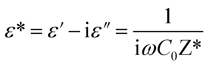
The permittivity measurements were performed to investigate the dielectric properties of the prepared samples. The complex dielectric permittivity can be expressed according to Mott's theory by the following equation:43
 |
5 |
where: ω = 2πf is the angular frequency, C0 is the open capacity of the capacitor, and ε′ (ε′′), is the real (imaginary) part of the dielectric permittivity.
3.4.1. Real part of dielectric permittivity
Fig. 5a and b presents the spectra of the real permittivity (ε′) over a wide range of frequencies at different temperatures for the samples  (x = 0.05 and x = 0.1). It can be noted that ε′ increases with decreasing frequency and increasing temperature for both samples, this finding specifies strong dielectric dispersion. This independence is due to the disability of the electric dipoles to follow the rapid variation of the applied electric field. Indeed, the high value of ε′ at low frequencies is mainly linked to the supply of electronic, spatial, interfacial and ionic charges, which are generally accompanied by the appearance of dielectric relaxation. Therefore, the dielectric dispersion observed in the low-frequency region is attributed to interfacial polarization, since electronic and atomic polarizations remain unchanged in this frequency range.44 Since dipoles are not able to orient themselves at low temperature, the increase in ε′ with temperature is associated to the fact that orientation polarization is related to the thermal motion of molecules.45
Fig. 5. The real permittivity spectra over a wide range of frequencies at different temperatures for the  (x = 0.05 (a) and x = 0.1 (b)) nanoparticles. Example fit of the (ε′) for (x = 0.05 (c) and x = 0.1 (d)) at T = 433 K.

The experimental data of the dielectric constant (ε′) were adjusted using the modified Debye function given by the following expression:46
 |
6 |
with: τ is the average relaxation time, α is a constant, ε′0 is the dielectric constant at low frequency, and ε′∞ is the dielectric constant at high frequency.
As clearly seen from Fig. 5c and d, the theoretical fit is strongly agree with the experimental data indicating the adequacy of the used modified Debye function. In this regard, the extracted parameters from the fitting process for the two studied compounds are illustrated in Table 1.
The extracted fitting parameters of the dielectric constant for samples (a) x = 0.05 and (b) x = 0.1.
| T(K) | ε′∞ | ε′0 | τ(×10−4 s) | α |
|---|---|---|---|---|
| a | ||||
| 313 | 286.228 | 533.030 | 197.9 | 0.606 |
| 333 | 285.477 | 449.166 | 110.5 | 0.597 |
| 353 | 286.219 | 381.550 | 14.8 | 0.612 |
| 373 | 286.580 | 370.775 | 9.491 | 0.619 |
| 393 | 286.783 | 367.731 | 7.788 | 0.623 |
| 413 | 287.049 | 364.857 | 6.308 | 0.627 |
| 433 | 287.857 | 358.106 | 3.642 | 0.643 |
| 453 | 287.500 | 384.279 | 9.158 | 0.624 |
| 473 | 289.088 | 354.958 | 1.981 | 0.671 |
| 493 | 289.146 | 379.135 | 4.182 | 0.651 |
| 513 | 289.837 | 396.356 | 4.990 | 0.652 |
| 533 | 291.152 | 391.738 | 2.721 | 0.680 |
| 553 | 291.540 | 392.361 | 1.607 | 0.698 |
| 573 | 292.296 | 408.412 | 1.529 | 0.708 |
| 593 | 294.162 | 448.053 | 2.451 | 0.697 |
| 613 | 295.173 | 486.198 | 3.086 | 0.688 |
| 633 | 296.124 | 507.949 | 2.919 | 0.685 |
| 653 | 295.475 | 499.068 | 1.932 | 0.680 |
| b | ||||
| 313 | 303.380 | 2229.150 | 3242.1 | 0.611 |
| 333 | 305.182 | 1813.746 | 1158.4 | 0.617 |
| 353 | 305.462 | 1584.427 | 365.2 | 0.622 |
| 373 | 307.185 | 960.237 | 31.1 | 0.636 |
| 393 | 308.175 | 854.618 | 11.4 | 0.645 |
| 413 | 309.128 | 819.915 | 6.217 | 0.651 |
| 433 | 309.299 | 814.972 | 4.141 | 0.652 |
| 453 | 309.151 | 825.538 | 3.019 | 0.651 |
| 473 | 307.325 | 852.730 | 2.458 | 0.644 |
| 493 | 304.109 | 889.698 | 2.146 | 0.636 |
| 513 | 297.307 | 958.701 | 2.226 | 0.623 |
| 533 | 284.217 | 1071.842 | 2.984 | 0.606 |
| 553 | 287.775 | 1072.210 | 2.085 | 0.609 |
| 573 | 280.154 | 1135.673 | 2.174 | 0.602 |
| 593 | 275.466 | 1344.296 | 4.815 | 0.591 |
| 613 | 281.412 | 1170.767 | 1.666 | 0.599 |
| 633 | 298.463 | 1311.502 | 3.425 | 0.596 |
| 653 | 314.602 | 1193.628 | 2.113 | 0.607 |
3.4.2. Imaginary part of dielectric permittivity
Fig. 6 exhibits the variation of the imaginary part (ε′′) of the complex permittivity versus frequency at different temperatures for the two compounds  (x = 0.05 (a) and x = 0.1 (b)), respectively. It is clear that ε′′ presents high values in the low-frequency region and decreases rapidly with increasing frequency within the presence of any relaxation peak. This feature is indicative of non-Debey behavior.47
Fig. 6. The variation of the imaginary part of the permittivity as a function of frequency at different temperatures for the  (x = 0.05 (a) and x = 0.1 (b)) samples, Fig. 6 c and d ln (ε′′) as a function of ln(ω) at different temperatures for (x = 0.05 (c) and x = 0.1 (d)).

In addition, as seen in Fig. 6c and d, the imaginary part of dielectric constant (ε′′) can be represented in a logarithmic variation ln(ε′′) as a function of ln(ω) at different temperatures according to the following expression given by Giuntini et al.:48
 |
7 |
Which can be rephrased as follows:49
| ε′′ = B(T)·ωm(T) | 8 |
In eqn (7), εs is the static dielectric constant, ε∞ the dielectric constant at “infinitely high” frequencies, KB is Boltzmann's constant, N is the density of localized states at which carriers exist, n is the number of polarons involved in the charge transfer process, e is an electronic charge, and WM is the energy required to move the electron from site to infinity (that's to say the energy necessary for charge carriers to cross over the potential barrier).
Then, in eqn (8), B(T) is a constant that depends only on temperature and m denotes an exponent describing the number of charge carriers, which is given by:50
 |
9 |
The calculated values of m as a function of temperature are collated in Fig. 7a and b. The same type of evolution has been observed in other compounds.51,52
Fig. 7. The exponent (m) calculated as a function of temperature for the  samples.

As shown in Fig. 7a and b, for x = 0.05, the values of m are proportional to the temperature, which matches the non-overlapping small polaron tunneling (NSPT)53 model, and then decrease with increasing temperature, suggesting the (CBH) model. Nevertheless, for x = 0.1, it is clear that m decreases with increasing temperature. Therefore, the correlated barrier hopping (CBH) model is the predominant mechanism. These findings are in good agreement with our previously published results regarding the electrical investigation of these two material.19
The temperature dependence of the real ε′ and imaginary ε′′ permittivity as a function of temperature at different frequencies (0.1 KHz, 1 KHz, 10 KHz, and 1 MHz) for the two compounds is illustrated in Fig. 8 and 9. As clearly seen, ε′ and ε′′ are independent of frequencies and temperatures over a small temperature range, then they gradually increase as the temperature increases. Furthermore, the interfacial polarization is known, as it increases with increasing temperature while the dipole polarization decreases with temperature.54,55 The observed increase in dielectric constant with the temperature at low frequencies confirms the domination of the interfacial polarization contribution to the dielectric constant in the studied materials.56
Fig. 8. The real permittivity as a function of temperature at different frequencies (0.1 KHz, 1 KHz, 10 KHz and 1 MHz) for the  (x = 0.05 (a) and x = 0.1 (b)) samples.

Fig. 9. The temperature dependence of the imaginary permittivity as a function of temperature for the  (x = 0.05 (a) and x = 0.1 (b)) compounds.

3.4.3. Loss factor
The dielectric loss factor expresses the ratio of the imaginary part of dielectric permittivity (ε′′) and the real part of dielectric permittivity (ε′), i.e.:
 |
10 |
where the angle δ is the phase difference between the applied electric field and the induced current.
Dielectric loss is known to occur when bias lags behind the applied AC field and can be caused by defects in the crystal lattice of grain boundaries, and impurities.57 The density of material also influences the variation in dielectric losses; for example, high porosity (low density) results in low dielectric constant and higher dielectric losses.58 The frequency dependence at different temperatures of the loss factor for the two samples is plotted in Fig. 10. Similar to ε′, tanδ values are important at low frequencies and gradually reduce at high frequencies until reaching a lower saturated value. The losses are minimized at high frequencies and the dipoles contribute to the polarization because their polarization can orient with the electric field due to their high conductivity.19,58 Thus, we notice that the value of the dielectric loss increases with an increase in temperature due to the electrical conductivity.59
Fig. 10. The frequency dependence at different temperatures of the loss factor for the two  (x = 0.05 (a) and x = 0.1 (b)) samples.

In this context, these results suggest that the two samples can be used in various technological applications, including fuel cells, ceramic technology, and microwave technology.60
3.4.4. Modulus analysis
The complex electrical modulus (M*) allows the study of the relaxation process and the dynamics of ions as a function of frequency and temperature.M* can be determined from the dielectric permittivity using the following formula:61
 |
11 |
Therefore, the real electric modulus (M′) and the imaginary electric modulus (M′′) can be expressed as follow:
| M′ = 2πfC0Z′′ | 12 |
| M′′ = 2πfC0Z′ | 13 |
where: C0 = ε0. (S/e) denotes the cell′s vacuum capacitance, ε0 = 8.854 10−12 F m−1 is the free space permittivity.
3.4.4.1. Real part of modulus
Fig. 11a and b shows the frequency dependence of the real part (M′) of the complex modulus as a function of frequency at different temperatures of the two prepared compounds.
Fig. 11. The frequency dependence of the real part of the complex modulus as a function for the two  (x = 0.05 (a) and x = 0.1 (b)) compounds.

It is worth noting that the values of M′ curves increase gradually until merging at the high-frequency range for the two compound. This confirms that the electrodes polarization phenomena does not contribute to the relaxation process and can be ignored when the electric field, is evaluated in this form.62
3.4.4.2. Imaginary part of modulus
The imaginary part of the electric modulus (M′′) as a function of frequency at different temperatures for the two materials is presented in Fig. 12a and b, to better understand dielectric relaxations. All the M′′ plots prove a maximum at a specific frequency called the relaxation frequency (fr). With increasing temperature, this maximum shifted to higher frequencies, implying that the relaxation is as temperature-dependent process.63 Several research articles64,65 have also reported similar results. Indeed, at low frequencies, we can see the presence of a pure conduction process66 in which ions can move freely over long distances. As the M′′ peaks move to higher frequencies, the ions are confined to only localized motion, which corresponds to carrier hopping over short distances.67 The experimental data of the M′′ for different temperatures were fitted with an approximate frequency representation of the Kohlrausch–Williams–Watts (KWW) function, proposed by Bergman:68
 |
14 |
where: Mmax′′ is the maximum value of the modulus peak, fmax is the Mmax′′ corresponding frequency, and (0 <β < 1) is the factor that appears in the empirical Kohlrausch function providing information on the type of dielectric relaxation which can be either Debye type or non-Debye type.69 In another hand, the temperature dependence of β is feature in Fig. 13a and b proving a continuous decrease up to 393 K than an increase for x = 0.05 (curve (a)), and for x = 0.1 (curve (b)), β behaves and increases with increasing temperature. Furthermore, Fig. 13c and d shows that the theoretical calculation fit agrees well with the experimental data.
Fig. 12. The imaginary part of the electric modulus as a function of frequency for the  (x = 0.05 (a) and x = 0.1 (b)) compounds.

Fig. 13. Temperature dependence of the β value for the two  (x = 0.05 (a) and x = 0.1 (b)) compounds. Example adjustment of the (M′′) for compounds (x = 0.05 (c) and x = 0.1 (d)) at T = 433 K.

When plotting the variation of the relaxation frequency (fmax) as a function of the inverse of the absolute temperature (1000/T), as seen in Fig. 14, it should be noted that this variation presents an activated behavior, according to following Arrhenius law:70
 |
15 |
where: KB is Boltzmann's constant, Ea denotes the activation energy required for the dielectric relaxation, and f0 is the pre-exponential factor.
Fig. 14. The variation of the relaxation frequency (fmax) as a function of (1000/T) for the two  (x = 0.05 (a) and x = 0.1 (b)) compounds.

The extracted values of the activation energy are: Ea = 0.610 eV and Ea = 0.419 eV respectively for x = 0.05 and x = 0.1, proving a decrease with increase in the Ag amount.
3.4.5. Complex polarizability studies
To better understand the phenomena of dielectric relaxation, the complex polarizability (α*), proposed by Scaife,71 was then focused, which is defined as follows:
 |
16 |
Where α′ and α′′ are the real and imaginary parts of the complex polarizability α*.
Accordingly, we can easily get the imaginary parts α′′ from eqn (16):50
 |
17 |
The complex polarizability gives proper weight to all polarization mechanisms and provides an easy way to compare the dielectric behavior of different substances.
On this point, Fig. 15 represents the variation of α′′ versus frequency at different temperature and highlights that a well separated relaxation peak with a maximum which shifts towards higher frequencies. According to these finding we displayed, in Fig. 16, the plot of (ln (fmax)) as a function of the inverse temperature of (1000/T).
Fig. 15. The imaginary part of complex polarizability as a function of frequency for the  (x = 0.05 (a) and x = 0.1 (b)) compounds.

Fig. 16. The variation of (ln (fmax)) versus of (1000/T) for the  (x = 0.05 (a) and x = 0.1 (b)) compounds.

The extracted activation energies are about is for 0.569 and 0.41 eV respectively for x = 0.05 and x = 0.1 which are almost the same as those extracted from the module analysis.
4. Conclusion
In summary, we have studied the optical and dielectric properties of  (x = 0.05 and x = 0.1) spinels prepared by sol-gel auto-combustion process. Both compounds crystallize in the cubic structure of space group Fd3̄m and exhibit a minority of (Ag) phase, according to the XRD measurements. In addition, FTIR spectroscopy analysis confirmed the formation of spinel structured compounds. The Kubelka–Munk formula is used to calculate the absorption coefficient, where the optical band gap is determined by the Tauc model. The calculated gap energy values are 4.3 eV for x = 0.05 and 4 eV for x = 0.1, indicating semiconductor behavior for both samples, which are better suited for applications as photodetectors, optoelectronics, and photovoltaics. The activation energies estimated from the modulus were found to be 0.599 eV for x = 0.05 and 0.412 eV for = 0.1, which is in agreement with the values obtained from the complex polarizability plot, in effect demonstrating that the charge carriers involved in the conduction and relaxation processes are the same.
Conflicts of interest
There are no conflicts to declare.
References
- Verwey E. J. W. Heilmann E. L. J. Chem. Phys. 1947;15:174–180. doi: 10.1063/1.1746464. [DOI] [Google Scholar]
- Miron I. Enache C. Vasile M. Grozescu I. Phys. Scr. 2012;2012:014064. doi: 10.1088/0031-8949/2012/T149/014064. [DOI] [Google Scholar]
- Yong X. Ping F. Baohua Z. Juan G. Lin Z. Xuehua W. Mater. Lett. 2014;123:142–144. doi: 10.1016/j.matlet.2014.03.013. [DOI] [Google Scholar]
- Ciupina V. Carazeanu I. Prodan G. J. Optoelectron. Adv. Mater. 2004;6:1317–1322. [Google Scholar]
- Kumar M. Seshagiri T. K. Mohapatra M. Natarajan V. Godbole S. V. J. Lumin. 2012;132:2810–2816. doi: 10.1016/j.jlumin.2012.04.033. [DOI] [Google Scholar]
- Komahal F. F. Nagabhushana H. Basavaraj R. B. Darshan G. P. Prasad B. D. Opt. Mater. 2018;84:536–544. doi: 10.1016/j.optmat.2018.06.058. [DOI] [Google Scholar]
- Kumar M. Natarajan V. Godbole S. V. Bull. Mater. Sci. 2014;37:1205–1214. doi: 10.1007/s12034-014-0063-9. [DOI] [Google Scholar]
- Fu P. Wang Z. Lin Z. Liu Y. Roy V. A. J. Mater. Sci.: Mater. Electron. 2017;28:9589–9595. doi: 10.1007/s10854-017-6707-y. [DOI] [Google Scholar]
- Siragam S. Dubey R. S. Pappula L. Mater. Today: Proc. 2021;45:2091–2095. [Google Scholar]
- Zou L. Li F. Xiang X. Evans D. G. Duan X. Chem. Mater. 2006;18:5852–5859. doi: 10.1021/cm0606124. [DOI] [Google Scholar]
- Tsai M.-T. Chang Y.-S. Huang B. Pan B.-Y. Ceram. Int. 2013;39:3691–3697. doi: 10.1016/j.ceramint.2012.10.201. [DOI] [Google Scholar]
- Parya T. K. Bhattacharyya R. K. Banerjee S. Adhikari U. B. Ceram. Int. 2010;36:1211–1215. doi: 10.1016/j.ceramint.2010.01.013. [DOI] [Google Scholar]
- Zawadzki M. Solid State Sci. 2006;8:14–18. doi: 10.1016/j.solidstatesciences.2005.08.006. [DOI] [Google Scholar]
- Agarwal H. Yadav T. P. Srivastava O. N. Shaz M. A. Ceram. Int. 2017;43:16986–16992. doi: 10.1016/j.ceramint.2017.09.106. [DOI] [Google Scholar]
- Wrzyszcz J. Zawadzki M. Trawczyński J. Grabowska H. Miśta W. Appl. Catal., A. 2001;210:263–269. doi: 10.1016/S0926-860X(00)00821-8. [DOI] [Google Scholar]
- Kingsley J. J. Suresh K. Patil K. C. J. Mater. Sci. 1990;25:1305–1312. doi: 10.1007/BF00585441. [DOI] [Google Scholar]
- Pathak N. Gupta S. K. Sanyal K. Kumar M. Kadam R. M. Natarajan V. Dalton Trans. 2014;43:9313–9323. doi: 10.1039/C4DT00741G. [DOI] [PubMed] [Google Scholar]
- Pan Q. Ye S. Yang D. Qiu J. Dong G. Mater. Res. Bull. 2017;93:310–317. doi: 10.1016/j.materresbull.2017.04.045. [DOI] [Google Scholar]
- Amghar M. Bougoffa A. Trabelsi A. Oueslati A. Dhahri E. RSC Adv. 2022;12:15848–15860. doi: 10.1039/D2RA01800D. [DOI] [PMC free article] [PubMed] [Google Scholar]
- Kumari P. Dwivedi Y. Bahadur A. Optik. 2018;154:126–132. doi: 10.1016/j.ijleo.2017.10.023. [DOI] [Google Scholar]
- Anand G. T. Kennedy L. J. Vijaya J. J. Kaviyarasan K. Sukumar M. Ceram. Int. 2015;41:603–615. doi: 10.1016/j.ceramint.2014.08.109. [DOI] [Google Scholar]
- Staszak W. Zawadzki M. Okal J. J. Alloys Compd. 2010;492:500–507. doi: 10.1016/j.jallcom.2009.11.151. [DOI] [Google Scholar]
- Ianoş R. Lazău R. Lazău I. Păcurariu C. J. Eur. Ceram. Soc. 2012;32:1605–1611. doi: 10.1016/j.jeurceramsoc.2011.12.028. [DOI] [Google Scholar]
- Duan X. Yuan D. Sun Z. Sun H. Xu D. Lv M. J. Cryst. Growth. 2003;252:4–8. doi: 10.1016/S0022-0248(03)00835-2. [DOI] [Google Scholar]
- Jamal E. M. A. Kumar D. S. Anantharaman M. R. Bull. Mater. Sci. 2011;34:251–259. doi: 10.1007/s12034-011-0071-y. [DOI] [Google Scholar]
- Motloung S. V. Dejene F. B. Swart H. C. Ntwaeaborwa O. M. J. Sol-Gel Sci. Technol. 2014;70:422–427. doi: 10.1007/s10971-014-3302-z. [DOI] [Google Scholar]
- Motloung S. V. Tsega M. Dejene F. B. Swart H. C. Ntwaeaborwa O. M. Koao L. F. Motaung T. E. Hato M. J. J. Alloys Compd. 2016;677:72–79. doi: 10.1016/j.jallcom.2016.03.170. [DOI] [Google Scholar]
- Abu-Khadra A. S. Taha A. M. Abdel-Ghany A. M. Abul-Magd A. A. Ceram. Int. 2021;47:26271–26279. doi: 10.1016/j.ceramint.2021.06.036. [DOI] [Google Scholar]
- Parhi P. Manivannan V. J. Eur. Ceram. Soc. 2008;28:1665–1670. doi: 10.1016/j.jeurceramsoc.2007.11.005. [DOI] [Google Scholar]
- Huang S. Wei Z. Wu X. Shi J. J. Alloys Compd. 2020;825:154004. doi: 10.1016/j.jallcom.2020.154004. [DOI] [Google Scholar]
- Sofia Nirmala T. Iyandurai N. Yuvaraj S. Sundararajan M. Mater. Res. Express. 2020;7:046104. doi: 10.1088/2053-1591/ab7a7a. [DOI] [Google Scholar]
- Peymanfar R. Fazlalizadeh F. Chem. Eng. J. 2020;402:126089. doi: 10.1016/j.cej.2020.126089. [DOI] [Google Scholar]
- Tangcharoen T. T-Thienprasert J. Kongmark C. Int. J. Appl. Ceram. Technol. 2021;18:1125–1143. doi: 10.1111/ijac.13765. [DOI] [Google Scholar]
- Kumar K. Ramamoorthy K. Koinkar P. M. Chandramohan R. Sankaranarayanan K. J. Nanopart. Res. 2007;9:331–335. doi: 10.1007/s11051-006-9108-3. [DOI] [Google Scholar]
- Kumar K. Ramamoorthy K. Koinkar P. M. Chandramohan R. Sankaranarayanan K. J. Cryst. Growth. 2006;289:405–407. doi: 10.1016/j.jcrysgro.2005.11.007. [DOI] [Google Scholar]
- Noor H. Riaz S. Iram M. M. Siddiqi A. Naseem S. Key Engineering Materials. Trans Tech Publ. 2018;778:217–224. [Google Scholar]
- Akika F. Z. Benamira M. Lahmar H. Tibera A. Chabi R. Avramova I. Suzer Ş. Trari M. J. Photochem. Photobiol., A. 2018;364:542–550. doi: 10.1016/j.jphotochem.2018.06.049. [DOI] [Google Scholar]
- Moustafa M. G. Morshidy H. Mohamed A. R. El-Okr M. M. J. Non-Cryst. Solids. 2019;517:9–16. doi: 10.1016/j.jnoncrysol.2019.04.037. [DOI] [Google Scholar]
- Morshidy H. Y. Abd El-Fattah Z. M. Abul-Magd A. A. Hassan M. A. Mohamed A. R. Opt. Mater. 2021;113:110881. doi: 10.1016/j.optmat.2021.110881. [DOI] [Google Scholar]
- Massoudi J. Smari M. Nouri K. Dhahri E. Khirouni K. Bertaina S. Bessais L. RSC Adv. 2020;10:34556–34580. doi: 10.1039/D0RA05522K. [DOI] [PMC free article] [PubMed] [Google Scholar]
- Chand P. Vaish S. Kumar P. Phys. B. 2017;524:53–63. doi: 10.1016/j.physb.2017.08.060. [DOI] [Google Scholar]
- Herve P. Vandamme L. K. J. Infrared Phys. Technol. 1994;35:609–615. doi: 10.1016/1350-4495(94)90026-4. [DOI] [Google Scholar]
- Ahmed M. A. Okasha N. Kershi R. M. Mater. Chem. Phys. 2009;113:196–201. doi: 10.1016/j.matchemphys.2008.07.032. [DOI] [Google Scholar]
- Zaouali A. Dhahri A. Boughariou A. Dhahri E. Barillé R. Costa B. F. O. Khirouni K. J. Mater. Sci.: Mater. Electron. 2021;32:1221–1232. doi: 10.1007/s10854-020-04895-2. [DOI] [Google Scholar]
- Yahia I. S. Hegab N. A. Shakra A. M. Al-Ribaty A. M. Phys. B. 2012;407:2476–2485. doi: 10.1016/j.physb.2012.03.049. [DOI] [Google Scholar]
- Kakade S. G. Ma Y.-R. Devan R. S. Kolekar Y. D. Ramana C. V. J. Phys. Chem. C. 2016;120:5682–5693. doi: 10.1021/acs.jpcc.5b11188. [DOI] [Google Scholar]
- Assoudi N. Hzez W. Dhahri R. Walha I. Rahmouni H. Khirouni K. Dhahri E. J. Mater. Sci.: Mater. Electron. 2018;29:20113–20121. doi: 10.1007/s10854-018-0143-5. [DOI] [Google Scholar]
- Giuntini J. C. Zanchetta J. V. Jullien D. Eholie R. Houenou P. J. Non-Cryst. Solids. 1981;45:57–62. doi: 10.1016/0022-3093(81)90089-2. [DOI] [Google Scholar]
- Seyam M. A. M. Appl. Surf. Sci. 2001;181:128–138. doi: 10.1016/S0169-4332(01)00378-6. [DOI] [Google Scholar]
- Taher Y. B. Oueslati A. Khirouni K. Gargouri M. J. Cluster Sci. 2015;26:1655–1669. doi: 10.1007/s10876-015-0865-y. [DOI] [Google Scholar]
- Abdallah F. B. Benali A. Azizi S. Triki M. Dhahri E. Graça M. P. F. Valente M. A. J. Mater. Sci.: Mater. Electron. 2019;30:8457–8470. doi: 10.1007/s10854-019-01166-7. [DOI] [Google Scholar]
- Hamdi R. Khelifi J. Walha I. Hzez W. Dhahri E. J. Low Temp. Phys. 2021;203:158–179. doi: 10.1007/s10909-021-02565-z. [DOI] [Google Scholar]
- Abdallah F. B. Benali A. Azizi S. Triki M. Dhahri E. Graça M. P. F. Valente M. A. J. Mater. Sci.: Mater. Electron. 2019;30:8457–8470. doi: 10.1007/s10854-019-01166-7. [DOI] [Google Scholar]
- Soibam I. Phanjoubam S. Sharma H. B. Sarma H. N. K. Laishram R. Prakash C. Solid State Commun. 2008;148:399–402. doi: 10.1016/j.ssc.2008.09.029. [DOI] [Google Scholar]
- Saafan S. A. Assar S. T. J. Magn. Magn. Mater. 2012;324:2989–3001. doi: 10.1016/j.jmmm.2012.04.037. [DOI] [Google Scholar]
- Saha S. Sinha T. P. J. Appl. Phys. 2006;99:014109. doi: 10.1063/1.2160712. [DOI] [Google Scholar]
- Ahsan M. Z. Khan F. A. J. Phys. Sci. 2017;7:30–37. [Google Scholar]
- Mangalaraja R. V. Manohar P. Gnanam F. D. Awano M. J. Mater. Sci. 2004;39:2037–2042. doi: 10.1023/B:JMSC.0000017766.07079.80. [DOI] [Google Scholar]
- Gowreesan S. Ruban Kumar A. Appl. Phys. A: 2017;123:1–8. doi: 10.1007/s00339-017-1302-x. [DOI] [Google Scholar]
- Hadded A. Massoudi J. Dhahri E. Khirouni K. Costa B. F. O. RSC Adv. 2020;10:42542–42556. doi: 10.1039/D0RA08405K. [DOI] [PMC free article] [PubMed] [Google Scholar]
- Stearn A. E. Eyring H. J. Chem. Phys. 1937;5:113–124. doi: 10.1063/1.1749988. [DOI] [Google Scholar]
- Lin H. Hania R. P. Bloem R. Mirzov O. Thomsson D. Scheblykin I. G. Phys. Chem. Chem. Phys. 2010;12:11770–11777. doi: 10.1039/C001120G. [DOI] [PubMed] [Google Scholar]
- Kim J. S. J. Phys. Soc. Jpn. 2001;70:3129–3133. doi: 10.1143/JPSJ.70.3129. [DOI] [Google Scholar]
- Dutta A. Sinha T. P. Shannigrahi S. Phys. Rev. B. 2007;76:155113. doi: 10.1103/PhysRevB.76.155113. [DOI] [Google Scholar]
- Victor P. Bhattacharyya S. Krupanidhi S. B. J. Appl. Phys. 2003;94:5135–5142. doi: 10.1063/1.1606509. [DOI] [Google Scholar]
- Holderna-Natkaniec K. Sghaier M. O. M. Lawniczak P. Zdanowska-Frączek M. Wozniak-Braszak A. Chaabouni S. Polyhedron. 2015;85:131–136. doi: 10.1016/j.poly.2014.08.044. [DOI] [Google Scholar]
- Bougoffa A. Benali A. Bejar M. Dhahri E. Graça M. P. F. Valente M. A. Bessais L. Costa B. O. F. J. Alloys Compd. 2021;856:157425. doi: 10.1016/j.jallcom.2020.157425. [DOI] [Google Scholar]
- Bougoffa A. Massoudi J. Smari M. Dhahri E. Khirouni K. Bessais L. J. Mater. Sci.: Mater. Electron. 2019;30:21018–21031. doi: 10.1007/s10854-019-02472-w. [DOI] [Google Scholar]
- Rao K. S. Krishna P. M. Prasad D. M. Gangadharudu D. J. Mater. Sci. 2007;42:4801–4809. doi: 10.1007/s10853-006-0748-6. [DOI] [Google Scholar]
- Benali E. M. Benali A. Bejar M. Dhahri E. Graca M. P. F. Valente M. A. Costa B. F. O. J. Mater. Sci.: Mater. Electron. 2020;31:3197–3214. doi: 10.1007/s10854-020-02867-0. [DOI] [Google Scholar]
- Scaife B. K. P. Proc. Phys. Soc. 1963;81:124. doi: 10.1088/0370-1328/81/1/318. [DOI] [Google Scholar]