Abstract
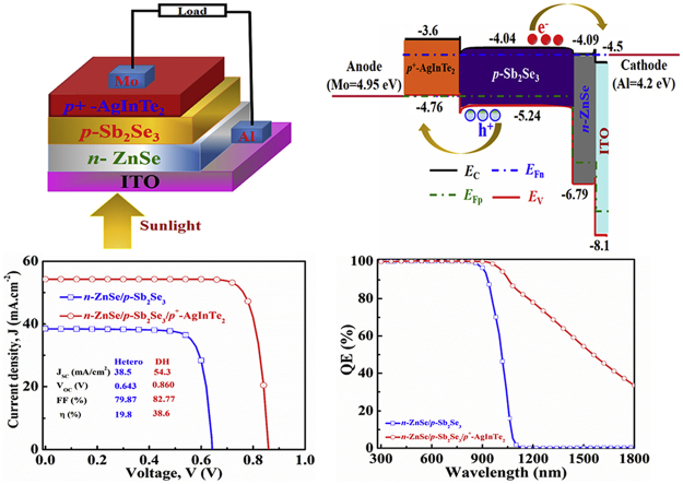
Here, we manifest the design and simulation of an n-ZnSe/p-Sb2Se3/p+-AgInTe2 dual-heterojunction (DH) solar cell which exhibits a prominent efficiency. The performance of the solar cell has been assessed with reported experimental parameters using SCAPS-1D simulator by varying thickness, doping concentration and defect density in each layer. The proposed structure shows an efficiency of 38.6% with VOC = 0.860 V, JSC = 54.3 mA/cm2 and FF = 82.77%, respectively. Such a high efficiency close to Shockley-Queisser (SQ) limit of DH solar cell has been achieved as a result of the longer wavelength photon absorption in the p+-AgInTe2 back surface field (BSF) layer through a tail-states assisted (TSA) two-step photon upconversion phenomenon. These results indicate hopeful application of AgInTe2 as a bottom layer in Sb2Se3-based solar cell to enhance the cell performance in future.
Keywords: Sb2Se3, AgInTe2, Dual-heterojunction, High efficiency, TSA upconversion
Graphical abstract
Highlights
-
•
A novel n-ZnSe/p-Sb2Se3/p+-AgInTe2 DH solar cell has been simulated using SCAPS-1D.
-
•
AgInTe2 BSF boosts PCE to 38.63% with VOC = 0.86V and JSC = 54.28 mA/cm2, respectively.
-
•
AgInTe2 shows its potential as BSF in Sb2Se3-based DH solar cell in near future.
Sb2Se3; AgInTe2; Dual-heterojunction; High efficiency; TSA upconversion.
1. Introduction
In photovoltaic, a challenging part for researchers is obtaining a significant value of power conversion efficiency (PCE) along with selecting abundant low-cost and eco-friendly materials for large area production. The silicon solar cells are still dominating the present commercial markets although the highest PCE of the solar cells is just over 26% which has been reported in 2017 (Yoshikawa et al., 2017). Besides, Silicon's high melting point and minimal tolerance to defects in the manufacturing process necessitate a pricey processing environment (Steinmann et al., 2015). Additionally, higher production cost of wafer-based silicon solar cell and reduction of residential uses due to its fragility are the matter of concerns for traditional cells (Pathak et al., 2015; Bhopal et al., 2017). As a consequence, choice of alternative materials and simple fabrication process for evolution of cells have received enormous attention to the researchers (Tyagi et al., 2013).
Recently, different types of solar cells based on materials or fabrication process have received a great interest for capability of providing significant efficiency. For instance, Cadmium telluride (CdTe) and CIGS based solar cells have clinched around 22% of PCE (Polman et al., 2016; Green et al., 2018; Jackson et al., 2016). Researchers have showed that recombination losses in the solar cells are resulted from the inherited dangling bonds at grain boundaries of Si as well as CdTe, CdS and CIGS that degrade the cell performance (Zhou et al., 2015). However, toxicity of materials in these types of solar cells are notable concerns for fabrication in industry due to health hazard (Pathak et al., 2015). Besides, scarcity of such elements causes rise in overall production cost. Therefore, replacement of cadmium containing materials has become a key concern (Pathak et al., 2014). Another option can be the hybrid methylammonium lead halide perovskite (MAPbX3) based solar cell that has an efficiency of 20.1% but it exhibits insufficient tolerance to defects. More recently, the highest efficiency of 25.2% has been attained for perovskite solar cell by increasing charged carrier management (Yoo et al., 2021). Nevertheless, efficient perovskite solar cell uses harmful element lead (Pb) and exhibits lack of stability at low temperatures (Steinmann et al., 2015).
Antimony selenide, Sb2Se3 which has the simple single phase non-cubic orthorhombic chalcogenide structure can be a prominent absorber that can meet up all the constraints discussed above (Steinmann et al., 2015; Chen et al., 2017; Mavlonov et al., 2020; Guo et al., 2019; Shen et al., 2020). Such crystal structure tends to yield ribbon-like or layered morphologies that outcome with thoroughly anisotropic charge transport. However, Sb2Se3 is abundant on earth in the form of mineral subnite. Its thermal evaporation property at low temperature and vacuum (350 °C and ∼8 mTorr, respectively) further contributes in cost minimization. It has also been found to exhibit excellent photovoltaic absorbance due to band gap of 1.1–1.3 eV and high absorption coefficient (>105 cm−1) at visible portion of solar spectrum. Besides, Sb2Se3 displays a good carrier mobility (). Literature reports indicate that both acceptor and donor types of impurities have been used for doping into the Sb2Se3 thin films that can be used as absorber layers in thin film solar cells. Many investigations have been performed on p and n type dopants of Sb2Se3 thin films. Among them, Cu, Sn and Fe can be employed as p-type dopants whereas halogen (I, Br, Cl) group can be utilized as n-type dopants in Sb2Se3 thin films (Mavlonov et al., 2020; Stoliaroff et al., 2020).
In 2009, researchers came up with 0.66% photo conversion efficiency introducing Sb2Se3 based solar cell structure (Messina et al., 2009). An efficiency of 6–7% for Sb2Se3-based solar cells have been obtained in experimental works through tuning selenization parameters and grain boundary inversion, respectively (Chen et al., 2018; Tang et al., 2019). Furthermore, contemporary work came into light with growth of nanorod array with a photo conversion efficiency of 9.2% (Li et al., 2019). However, simulation works have also been performed to provide guidelines for further improvement of Sb2Se3-based solar cells. According to recent simulation studies, the efficiency of the Sb2Se3-based solar cell can be reached to 23–29% by employing CdS window layer and CuO and BaSi2 BSF layers (Li et al., 2019; Ahmed et al., 2021).
Zinc Selenide (ZnSe) can be an alternative solution to substitute toxic CdS in window layer for heterojunction solar cells. The efficiency of a photovoltaic cell relies on avoiding the recombination of photo generated carriers and such sidestepping is done by adding a thin window layer of a wide band gap material (Krause et al., 1994; Kale et al., 2006; Yater et al., 1996). ZnSe provides a wider band gap of 2.7eV than CdS of 2.4 eV (Ahmed et al., 2021). Another disadvantage is CdS window comes up with higher surface roughness and lower transmittance that limit the efficiency of the practical solar cells (Kim et al., 2010). To the contrary, polycrystalline nature and high refractive index of ZnSe provide higher transmittance in visible and ultraviolet region of solar spectrum (Jones and Woods, 1976; Green et al., 2010). Furthermore, low reaction to humidity of ZnSe is an additional advantage in industrial production (Yater et al., 1996).
Crossing the different cohort of solar modules, heterojunction solar cells has entered into fourth generation with a goal of overcoming the barriers of theoretical expectation (Sharma et al., 2015). A heterojunction is fabricated by attaching an n-type layer with a p-type layer of dissimilar materials. The absorption of photons in the absorber layer results photocurrent through the generation of electron-hole pairs which are separated by the space charges at the pn junction. However, the photo conversion efficiency of single heterojunction cells cannot go beyond the SQ limit due to (i) thermal relaxation loss by high energy photon absorbed by a low band gap substance and (ii) below-band gap absorption loss by excitation failure of low energy photon to a high band gap material (Malinkiewicz et al., 2014; Yamaguchi et al., 2018).
An improvement can be achieved with imparting comparatively higher band gap top layer and lower band gap back surface layer with absorbing material (Rong et al., 2018). Similar concepts have been found to overcome SQ limit for dual-heterojunction solar cells (Martí and Luque, 2015). AgInTe2 is a potential ternary chalcopyrite material exhibiting a band gap of 0.96–1.16 eV which is just below the band gap of Sb2Se3 (Benseddik et al., 2020; El-Korashy et al., 1999). Such a value along with high absorption coefficient (4×104 cm−1 at an wavelength of 1095 nm) and also sub-band gap effects have brought it as a suitable candidate for back surface absorber layer (El-Korashy et al., 1999). Though several works have been found on AgInTe2 based solar cells, to the best of our knowledge, such a promising candidate has never been utilized as a BSF layer.
In this work, a novel Sb2Se3-based n-ZnSe/p-Sb2Se3/p+-AgInTe2 dual-heterojunction solar cell structure has been proposed and simulated with a view to provide longer wavelength light absorption and minimize photon loss in the back surface layer. The light trapping strategy and the reason of high efficiency have been illustrated with absorption of photon in Sb2Se3 absorber layer through tail-states assisted (TSA) two-step photon upconversion phenomenon in p+-AgInTe2 BSF as well as bottom absorber layer.
2. Design of proposed Sb2Se3-based dual-heterojunction and numerical simulation
2.1. Device structure
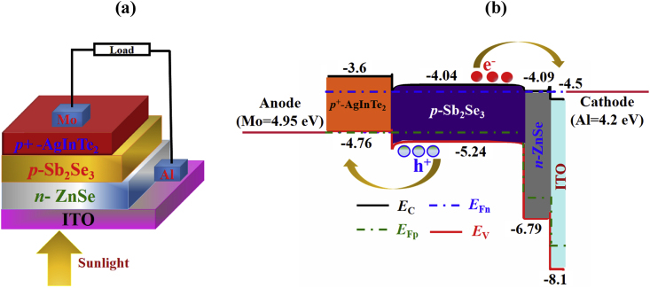
The schematic block diagram and illuminated energy band diagram of the proposed highly efficient Sb2Se3-based dual-heterojunction solar cell are visualized in Figure 1a and b, respectively. Herein, photons enter through the Indium tin oxide (ITO) coated glass substrate and n-type ZnSe window layer. The photons are then absorbed by p-type Sb2Se3 absorber layer. The EC and EV of ZnSe are 4.09 and 6.79 eV, respectively (Olopade et al., 2012; Samantilleke et al., 1998). On the other hand, the electron affinity and ionization potential of Sb2Se3 are 4.04 and 5.24 eV, respectively. Hence, it creates a possibility for n-type ZnSe and p-type Sb2Se3 to build a favorable pn junction. In addition, AgInTe2 is a semiconducting compound having a direct band gap of 0.96–1.16 eV which has already been reported as absorber layer with CdTe window combination (Benseddik et al., 2020). In this design, p+-type AgInTe2 has been employed to perform double role such as bottom absorber and back surface field (BSF) layer. Because of its high absorption coefficient (α) i.e sub-band gap absorption in the longer wavelength region, it is an efficient material as bottom absorber layer to absorb longer wavelength photons (El-Korashy et al., 1999; Vaidhyanathan et al., 1983). AgInTe2 has electron affinity and ionization potential of 3.6 eV and 4.76 eV, respectively making it a suitable candidate to form a pp+ junction with Sb2Se3. The quasi Fermi levels for electrons and holes are denoted as EFn and EFp, respectively as depicted in Figure 1b. In AgInTe2, the EFn level lies above the VB edge whereas EFp level lies below the CB edge in ZnSe. Therefore, photo-generated electrons are moved towards the n-type window layer and blocked by BSF layer. Consequently, photo-generated holes are blocked by window layer and moved towards p+-type BSF layer. Therefore, anode and cathode can easily collect holes and electrons, respectively from absorber layer. In this design, earth abundant metals Al and Mo are used as cathode and anode, respectively.
Figure 1.
The (a) schematic block diagram and (b) energy band diagram with illumination of n-ZnSe/p-Sb2Se3/p+-AgInTe2 dual-heterojunction solar cell.
2.2. Simulation model and physical parameters
The Sb2Se3-based n-ZnSe/p-Sb2Se3/p+-AgInTe2 dual-heterojunctionsolar cell was numerically simulated using a one-dimensional solar cell capacitance (SCAPS-1D) software developed by M. Burgelman et al. at the University of Gent, Belgium (Burgelman et al., 2004). This software analyzes solar cell structure by solving three basic equations of semiconductor i.e. Poisson's equation, the continuity equations for free holes and electrons and the drift-diffusion equation. The simulation was accomplished under the illumination of one sun with 100 mW/cm2 and the global air mass (AM) of 1.5G illumination spectrum at 300 K operating temperature. In this simulation, ideal values of series and shunt resistance were considered and radiative recombination coefficient was avoided. Gaussian energetic distribution was set for acceptor and donor defects for bulk layers and interface defects were also considered. Thermal velocity of 107 cm/s was set for window, absorber and BSF layer and surface recombination velocity was taken 107 cm/s for both metallic contacts. The absorption coefficient data for ZnSe, Sb2Se3 and AgInTe2 layer were collected from various literatures based on experimental works (El-Korashy et al., 1999; Adachi and Taguchi, 1991; El-Shair et al., 1991). It is noted that SCAPS software can automatically account the sub-band gap absorption effect on solar cell performance once the optical data are provided. The physical parameters for different layers used in this simulation are shown in Table 1, whereas interfaces parameters are shown in Table 2.
Table 1.
Physical parameters of n-ZnSe/p-Sb2Se3/p+-AgInTe2 dual-heterojunction solar cell used in this simulation.
| Parameters | ITO (Ahmmed et al., 2020) | n-ZnSe (Olopade et al., 2012; Samantilleke et al., 1998) | p-Sb2Se3 (Z. Q. Li et al., 2019) | p+-AgInTe2 (Benseddik et al., 2020; El-Korashy et al., 1999; Yang et al., 2017) |
|---|---|---|---|---|
| Layer type | Substrate | Window | Absorber | BSF |
| aThickness [μm] | 0.05 | 0.1 | 1.0 | 0.5 |
| Band gap, [eV] | 3.6 | 2.7 | 1.2 | 1.16 |
| Electron affinity, χ [eV] | 4.5 | 4.09 | 4.04 | 3.6 |
| Dielectric permittivity, ε [relative] | 8.9 | 10 | 18 | 8.9 |
| Effective CB density, NC [cm−3] | 2.2×10¹⁸ | 1.5×10¹⁸ | 2.2×10¹⁸ | 3.66×10¹⁹ |
| Effective VB density, NV [cm−3] | 1.8×10¹⁹ | 1.8×10¹⁹ | 1.8×10¹⁹ | 1.35×10¹⁹ |
| Electron mobility, [cm2 V−1 s−1] | 50 | 50 | 15 | 1011 |
| Hole mobility, [cm2 V−1 s−1] | 10 | 20 | 5.1 | 887 |
| aDonor concentration, ND [cm−3] | 1.0×10²¹ | 1.0×10¹⁸ | 0 | 0 |
| aAcceptor concentration, NA [cm−3] | 1.0×10⁷ | 0 | 1.0×10¹⁵ | 3.5×10¹⁹ |
| Defect type | Acceptor | Acceptor | Donor | Neutral/Donor |
| Energetic distribution | Gaussian | Gaussian | Gaussian | Gaussian |
| Reference for defect energy level, Et | Above the highest EV | Above the highest EV | Above the highest EV | Above the highest EV |
| Energy with respect to Reference [eV] | 1.8 | 1.35 | 0.6 | 0.58 |
| aPeak defect density, N(t) [eV−1 cm−3] | 1.0×10¹⁴ | 1.0×10¹³ | 1.0×10¹³ | 1.0×10¹³ |
| Characteristic energy [eV] | 0.1 | 0.1 | 0.1 | 0.1 |
| Electron capture cross section for defect [cm2] | 10−15 | 10−15 | 10−15 | 10−15 |
| Hole capture cross section for defect [cm2] | 10−15 | 10−15 | 10−17 | 10−15 |
is a variable field.
Table 2.
Interface parameters used in this simulation.
| Parameters | ZnSe/Sb2Se3 interface | Sb2Se3/AgInTe2 interface |
|---|---|---|
| Defect type | Neutral | Neutral |
| Capture cross section for electrons [cm2] | 10−19 | 10−19 |
| Capture cross section for holes [cm2] | 10−19 | 10−19 |
| Energetic distribution | Single | Single |
| Reference for defect energy level, Et | Above the highest EV | Above the highest EV |
| Energy with respect to reference (eV) | 0.6 | 0.6 |
| Total defects (cm−2) | 1010 | 1010 |
3. Results and discussion
3.1. Performance of Sb2Se3-based solar cells
3.1.1. Role of Sb2Se3 absorber layer on PV parameters of n-ZnSe/p-Sb2Se3 solar cell
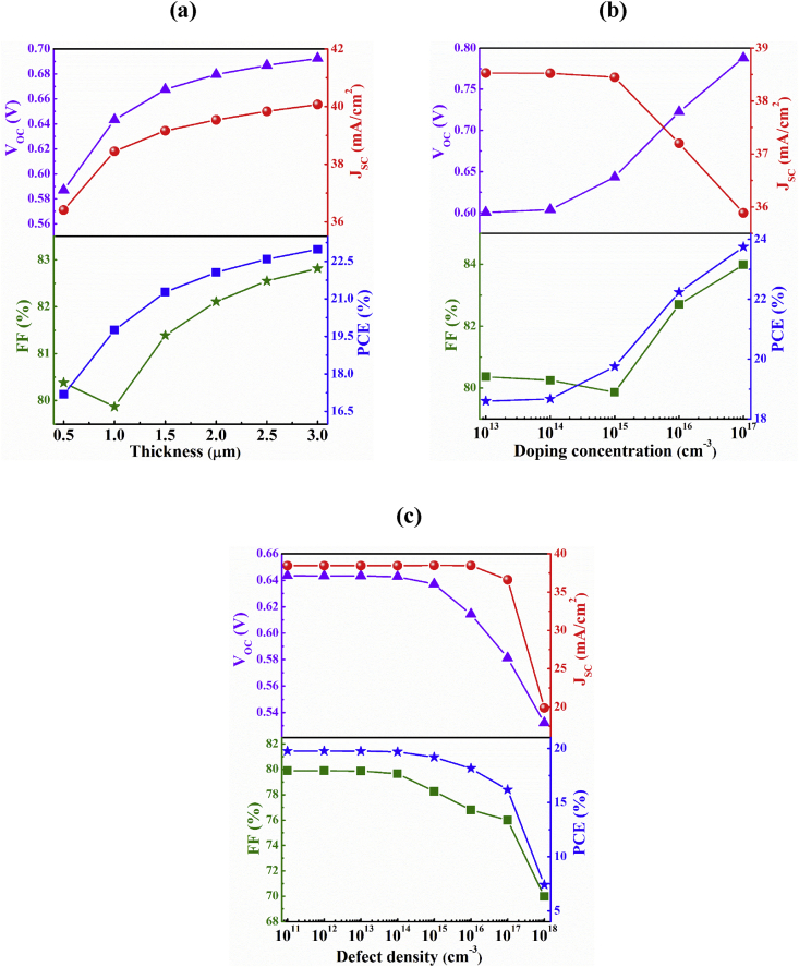
In this section, the impacts of thickness, carrier concentration and bulk defects of absorber layer on the proposed Sb2Se3-based solar cell without BSF layer have been studied. Figure 2a depicts the dependency of solar cell performance on thickness of Sb2Se3 absorber layer considering 1015 and 1013 cm−3 as acceptor concentration and defect density, respectively. Here, we observe that as the thickness of Sb2Se3 absorber layer is increased, all photovoltaic (PV) parameters boost as well. The short circuit, JSC has been risen up from 36.4 to 40.1 mA/cm2 with an increase in thickness from 0.5 to 3.0 μm. The increment of JSC is reasonable because thicker absorber layer can create more electron-hole pairs (EHPs) through absorbing more photons incident on it (Hossain et al., 2020). At the same time, open circuit voltage, VOC also increases with the thickness of the Sb2Se3 absorber layer. For instance, VOC goes from 0.587 to 0.693 V at an enlargement of absorber thickness from 0.5 to 3.0 μm. The obtained VOC of 0.680 V at 2.0 μm thickness of Sb2Se3 is consistent with the previous report (Kale et al., 2006). The fill factor (FF) and PCE have also ameliorated from 80.38 and 17.2 % to 82.82% and 22.9%, respectively at an increment of Sb2Se3 absorber from 0.5 to 3.0 μm. We consider 1.0 μm as the optimized thickness of the absorber Sb2Se3 layer to carry out further investigations.
Figure 2.
Performance dependency of n-ZnSe/p-Sb2Se3 solar cell on Sb2Se3 absorber layer parameters: (a) thickness, (b) doping concentration and (c) bulk defects.
The effect of acceptor concentration of Sb2Se3 absorber layer on PV parameters are shown in Figure 2b. The VOC rises from 0.601 to 0.788 V when the carrier concentration is increased from 1013 to 1017 cm−3. However, JSC is observed to downfall with the increase in carrier concentration. The recombination loss increases as a result of high doping concentration that affect the cell performance and a decrement of JSC occurres from 38.5 to 35.9 mA/cm2 due to the enhancement of carrier concentration from 1013 to 1017 cm−3 (Hossain et al., 2020; Watahiki et al., 2016). However, as the series resistance gets lowered at higher carrier concentration, FF rises from 80.37 to 84%. Consequently, the PCE enhances from 18.60 to 23.75% depending on upgradation of VOC and FF.
Defects play an important role in the performances of a solar cell. A number of investigations have been done on defects formation in Sb2Se3 for determining formation energy and transition levels that might be helpful for the improvement of the performance of Sb2Se3 based solar cells (Mavlonov et al., 2020; Savory and Scanlon, 2019; Stoliaroff et al., 2020). The variation of PV parameters with bulk defects of Sb2Se3 absorber layer is delineated in Figure 2c. To study the dependency of output parameters on defects of Sb2Se3 absorber layer, single donor type defects in the range from 1011 to 1018 cm−3 have been assumed. It is observed from the figure that the JSC is about 38.45 mA/cm2 and is almost independent on bulk defects of absorber up to a defect of 1016 cm−3. However, if the bulk defect is further increased to 1017 cm−3, JSC decreases to 36.6 mA/cm2 and the reduction of the photocurrent is about 1.8 mA/cm2. The photocurrent drastically plunges to 19.9 mA/cm2 at a defect of 1018 cm−3 owing to the increase in recombination current with defects (Kuddus et al., 2021b). The other parameters are also affected by the bulk defects. The Shockley-Read-Hall (SRH) recombination becomes the dominant recombination at high defects resulting inflation in the reverse saturation current and consequently VOC of the device reduces (Moon et al., 2020). Here, The VOC drops from 0.644 to 0.532 V when the defect density is raised from 1011 to 1018 cm−3. The FF also drops from 79.89 to 69.98% due to defects of absorber layer. As all the parameters gets reduced due to the increment of bulk defects of Sb2Se3 layer, the PCE of the solar cell also drastically turns down from 19.8% at defects of 1011 cm−3 to 7.4% at defects of 1018 cm−3. We have considered 1013 cm−3 as reasonable optimized defects for Sb2Se3 absorber layer.
The maximum efficiency of Sb2Se3-based solar cell without BSF layer is found to be about 23.8% with a high acceptor concentration of 1017 cm−3 and a thickness of 1.0 μm. Moreover, it has been observed that ZnSe window layer has negligible effects on the output parameters. Therefore, the optimized PCE of the Sb2Se3 solar cell without BSF layer is 19.8% with acceptor concentration and thickness of 1015 cm−3 and 1.0 μm, respectively.
3.1.2. Role of Sb2Se3 absorber layer on quantum efficiency of n-ZnSe/p-Sb2Se3 solar cell
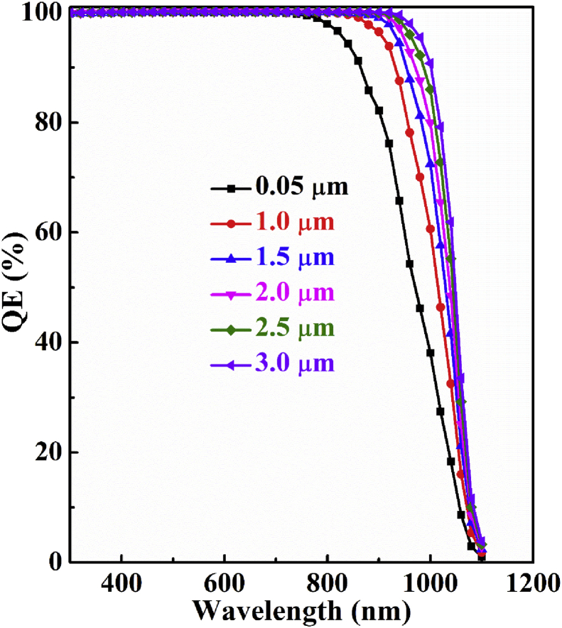
The quantum efficiency (QE) is a function of light wavelength (λ) which can be defined as the ratio of charge carriers produced by a solar cell to the number of incident photons on that cell (Hossain et al., 2021b; Moon et al., 2020). Figure 3 represents the simulated QE with respect to thickness of Sb2Se3 absorber layer of n-ZnSe/p-Sb2Se3 single heterojunction solar cell. It is noticed in the figure that QE improves gradually with the extension of Sb2Se3 absorber layer thickness as thicker absorber layer can capture more photons. Then all the curves associated different thickness downfall towards 0% at a particular higher wavelength when photon energy (hν) becomes lower than band gap (Eg) energy of Sb2Se3 absorber layer.
Figure 3.
Simulated QE dependence on Sb2Se3 absorber layer thickness of n-ZnSe/p-Sb2Se3 single-heterojunction solar cell.
3.2. Sb2Se3-based solar cell with AgInTe2 BSF layer
3.2.1. Role of AgInTe2layer on PV parameters of n-ZnSe/p-Sb2Se3/p+-AgInTe2dual-heterojunction solar cell
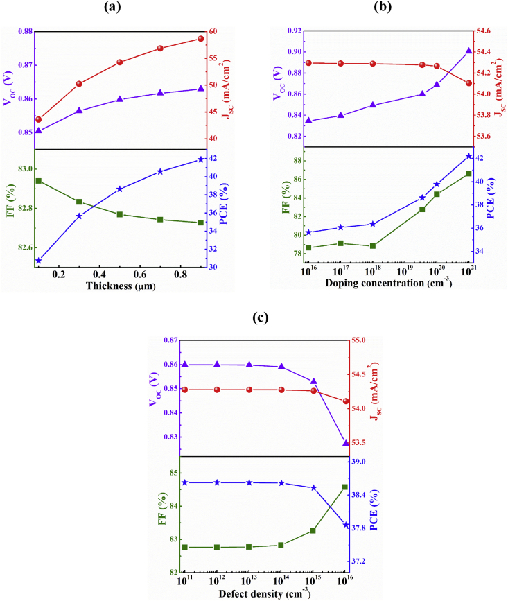
In this section, the influences of AgInTe2 layer on the designed n-ZnSe/p-Sb2Se3/p+-AgInTe2 dual-heterojunction structure have been explored. The thickness, doping concentration, and bulk defects of the AgInTe2 BSF layer have been varied in order to investigate the impact of this BSF layer as displayed in Figure 4.
Figure 4.
Dependency of the performance of n-ZnSe/p-Sb2Se3/p+-AgInTe2 dual-heterojunction solar cell on AgInTe2 BSF layer parameters: (a) thickness, (b) doping concentration and (c) bulk defects.
Figure 4a exhibits the thickness dependent PV parameters of n-ZnSe/p-Sb2Se3/p+-AgInTe2 dual-heterojunction solar cell. As observed, all of the output parameters significantly improve on account of employing AgInTe2 layer that performs dual role as BSF and bottom absorber layer. Here, JSC escalates from 38.5 to 54.3 mA/cm2 with an addition of 0.5 μm thick AgInTe2 layer. When the thickness of AgInTe2 is extended from 0.1 to 0.9 μm, JSC enhances from 43.6 to 58.7 mA/cm2. The significant growth of JSC relies on the absorption of longer wavelength photons by AgInTe2 layer through Tail-States-Assisted (TSA) two-steps photon upconversion process (Mostaque et al., 2022; Mondal et al., 2021; Kuddus et al., 2021a). In TSA upconversion process, two low-energy i.e. sub-band gap photons are absorbed in a sequence by Urbach tail-states of materials which provide extra EHPs. A material with preferable band gap, doping concentration and high absorption coefficient in longer wavelength region could result TSA upconversion process (Mostaque et al., 2022; Mondal et al., 2021; Hossain et al., 2021a, 2022). The detail qualitative discussion of the TSA upconversion process can be perceived in other work (Mostaque et al., 2022). Fortunately, AgInTe2 is a chalcopyrite material comprising a band gap of 1.16 eV (Malinkiewicz et al., 2014), high absorption coefficient of 103 cm−1 in the wavelength of 1800 nm (obtained from SCAPS extrapolation utilizing absorption coefficient data from experimental work) (Benseddik et al., 2020; El-Korashy et al., 1999) and also possesses high carrier concentration of 3.66 × 1019 cm3 (Yang et al., 2017). All of these factors make AgInTe2 a suitable candidate to participate in a TSA upconversion process. The VOC also improves from 0.640 to 0.840 V due to insertion of 0.5 μm AgInTe2 layer. The VOC gradually enhances from 0.851 at 0.1 μm to 0.863 V at 0.9 μm thickness of AgInTe2. The insertion of AgInTe2 layer produces high built-in potential in the Sb2Se3/AgInTe2 interface which contribute to the enhancement of the VOC (Hossain et al., 2021b; Mondal et al., 2021). The FF appears to be almost constant as a function of the thickness of AgInTe2. As JSC and VOC both rises with varying depth from 0.1 to 0.9 μm, a negligible change from 82.94 to 82.73% has been observed in FF. Eventually, the insertion of AgInTe2 BSF layer enriches the PCE from 30.8 to 41.9% as the width of BSF layer is expanded from 0.1 to 0.9 μm owing to the excessive gain in current and voltage. An enhancement of PCE from 19.8 to 38.6% has been observed at 0.5 μm thickness of AgInTe2 BSF layer.
Figure 4b delineates the performances of the proposed Sb2Se3-based DH solar cell structure with the variation of acceptor concentration (NA) of AgInTe2 layer from 1016 to 1021 cm−3 while maintaining the other parameters unchanged. It is observed from figure that the JSC is almost constant up to the concentration of 1020 cm−3. It slightly falls from 54.3 to 54.1 mA/cm2 due to high carrier concentration which may happened due to the parasitic free carrier absorption or high doping may have negative effect in TSA upconversion process in the BSF layer (Kuddus et al., 2021a). The VOC escalates from 0.835 to 0.901 V with increasing acceptor concentration from 1016 to 1021 cm−3of AgInTe2 layer. Since the built-in potential rises with additional NA, the enhancement of VOC with doping concentration is reasonable since higher built-in potential will the reduce recombination current (Hossain et al., 2020; Mostaque et al., 2022). This trend is also evident in FF and PCE which elevate from 78.65 and 35.7% to 86.62 and 42.2%, respectively for the increase of carrier concentration from 1016 to 1021 cm−3.
To investigate the influences of defect density of AgInTe2 BSF layer, on Sb2Se3-based double-heterojunction solar cell, neutral/donor types of defects have been assumed and varied it from 1011 to 1016 cm−3 considering other parameters same as specified in Tables 1 and 2. The variation of photovoltaic parameters with bulk defects of AgInTe2 layer is depicted in Figure 4c. The JSC shows almost constant behavior up to a defect level of 1015 cm−3 but then it has negligible decrement because of higher defects which obstruct to generate EHPs. The VOC also drops from 0.860 to 0.827 V owing to the increase of defect level from 1011 to 1016 cm−3. Since, both JSC and VOC fall with increasing bulk defects of AgInTe2 layer, FF is found to improve from 82.76 to 84.58%. The PCE has also decreased from 38.6% at defect density of 1011 cm−3 to 37.9% at defect density of 1016 cm−3. Hence, utilizing AgInTe2 as BSF as well as bottom absorber layer in Sb2Se3 solar cell with reasonable defects, it is possible to attain the Shockley-Queisser (SQ) efficiency limit for a dual-heterojunction solar cell.
3.2.2. Role of AgInTe2layer on quantum efficiency of n-ZnSe/p-Sb2Se3/p+-AgInTe2dual-heterojunction solar cell
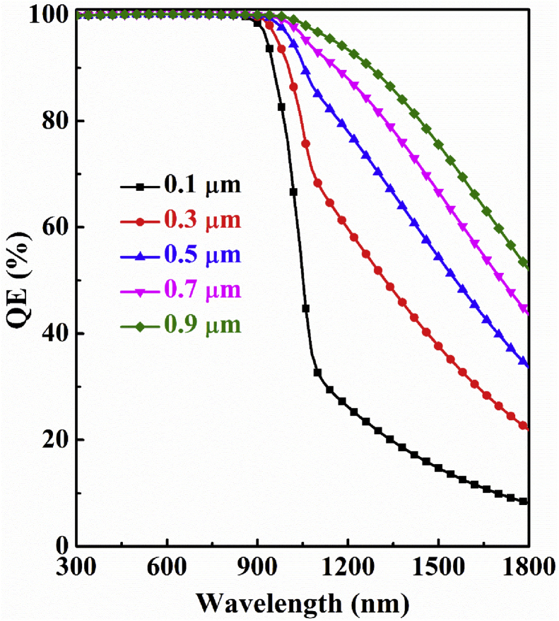
Figure 5 represents the simulated QE as a function of light wavelength for Sb2Se3-based dual-heterojunction solar cell with a varying thickness of AgInTe2 layer. It is noticed that, QE increases dramatically as the thickness of the AgInTe2 layer is gradually incremented from 0.1μm to 0.9 μm. In the longer wavelength range, for example, at 1800 nm, this device has a QE of over 30% at 0.5 m thickness, whereas 0% QE in absence of the AgInTe2 layer as observed in Figure 3. It clarifies the ability of AgInTe2 layer to capture longer wavelength photons as demonstrated by the TSA two-steps photon upconversion process in which the creation of additional EHPs plays a significant role behind this augmentation (Mostaque et al., 2022; Mondal et al., 2021; Kuddus et al., 2021a).
Figure 5.
Simulated QE dependence of n-ZnSe/p-Sb2Se3/p+-AgInTe2 dual-heterojunction solar cell on the thickness of AgInTe2layer.
3.3. The optimized performance of single and dual-heterojunction cells
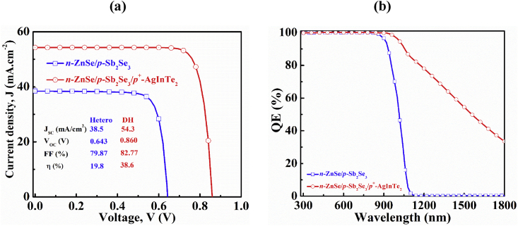
The current-voltage curves under illumination and quantum efficiency for Sb2Se3-based single n-p heterojunction and double n-p-p+ heterojunction solar cells are displayed in Fig. 6a and b, respectively. It is evident from Figure 6a that the installation of a p + -AgInTe2 layer revamps the cell performance substantially. The reason behind such an overshoot can be demonstrated with the TSA photon upconversion process where sub-band gap photons are occupied by the Urbach states (Mostaque et al., 2022; Mondal et al., 2021; Kuddus et al., 2021a). These low energy sub-band gap photons take part in generating electron-hole pairs contributing to the photocurrent (Yablonovitch et al., 1982; Wu and Williams, 1983). The degree of current enhancement and hence QE depend not only on Urbach energy but also on the band gap of the material. The generation of high built-in potential at the Sb2Se3/AgInTe2 interface further enhances the value of VOC (Hossain et al., 2021b). As a result, the efficiency has remarkably improved due to the addition of AgInTe2 as bottom layer. Figure 6b reveals that the QE in n-p heterojunction structure falls to 0% at the wavelength of 1100 nm whereas, it displays about 40% corresponding QE in the proposed n-p-p+ structure with the inclusion of AgInTe2 BSF layer. The QE seems to theoretically remain around 30% even for 1800 nm wavelength. This finding indicates that AgInTe2 could be a promising candidate for improving the PCE of Sb2Se3-based solar cells in near future.
Figure 6.
Simulated (a) light J-V and (b) QE curves of Sb2Se3-based single and dual-heterojunction solar cells.
4. Conclusion
The present work demonstrates the numerical simulation of Sb2Se3-based n-ZnSe/p-Sb2Se3/p+-AgInTe2 dual-heterojunction solar cell using SCAPS-1D software by incorporating interface defects and varying thickness, doping concentration and bulk defects in each layer. The simulation reveals that the incorporation of AgInTe2 which also serves as a bottom absorber layer can collect longer wavelength photons through TSA two-steps photon upconversion process, resulting a considerable enhancement in photocurrent. The optimized performance considering 0.1 μm thick n-ZnSe window and 1.0 μm p-Sb2Se3 absorber provides an efficiency of 19.8% that shoots up to 38.6% with JSC of 54.3 mA/cm2, VOC of 0.860 V and FF of 82.77%, respectively owing to the incorporation of only a 0.5 μm AgInTe2 BSF layer. Overall, the study suggests that AgInTe2 compound as a bottom layer displays strong potential for the enhancement of the efficiency of Sb2Se3-based solar cells in future.
Declarations
Author contribution statement
Bipanko Kumar Mondal: Conceived and designed the experiments; Performed the experiments; Analyzed and interpreted the data; Wrote the paper.
Shaikh Khaled Mostaque: Analyzed and interpreted the data; Wrote the paper.
Jaker Hossain: Conceived and designed the experiments; Contributed reagents, materials, analysis tools or data; Wrote the paper.
Funding statement
This research did not receive any specific grant from funding agencies in the public, commercial, or not-for-profit sectors.
Data availability statement
Data included in article/supplementary material/referenced in article.
Declaration of interests statement
The authors declare no conflict of interest.
Additional information
No additional information is available for this paper.
Acknowledgements
The authors highly appreciate Dr. Marc Burgelman, University of Gent, Belgium, for providing SCAPS 1D simulation software.
References
- Adachi S., Taguchi T. Optical properties of ZnSe. Phys. Rev. B. 1991;43:9569–9577. doi: 10.1103/physrevb.43.9569. [DOI] [PubMed] [Google Scholar]
- Ahmed S.R. Al, Sunny A., Rahman S. Performance enhancement of Sb2Se3 solar cell using a back surface field layer: a numerical simulation approach. Sol. Energy Mater. Sol. Cells. 2021;221:110919. [Google Scholar]
- Ahmmed S., Aktar A., Hossain J., Ismail A.B.M. Enhancing the open circuit voltage of the SnS based heterojunction solar cell using NiO HTL. Sol. Energy. 2020;207:693–702. [Google Scholar]
- Benseddik N., Belkacemi B., Boukabrine F., Ameur K., Mazari H., Boumesjed A., Benyahya N., Benamara Z. Numerical study of AgInTe2 solar cells using SCAPS. Adv. Mater. Process. Technol. 2020 [Google Scholar]
- Bhopal M.F., Lee D.W., Rehman A.U., Lee S.H. Past and future of graphene/silicon heterojunction solar cells: a review. J. Mater. Chem. C. 2017;5:10701–10714. [Google Scholar]
- Burgelman M., Verschraegen, Degrave J.S., Nollet P. Modeling thin-film devices. Prog. Photovoltaics Res. Appl. 2004;12:143–153. [Google Scholar]
- Chen C., Bobela D.C., Yang Y., Lu S., Zeng K., Ge C., Yang B., Gao L., Zhao Y., Beard M.C., Tang J. Characterization of basic physical properties of Sb2Se3 and its relevance for photovoltaics. Front. Optoelectron. 2017;10:18–30. [Google Scholar]
- Chen C., Li K., Chen S., Wang L., Lu S., Liu Y., Li D., Song H., Tang J. Efficiency improvement of Sb2Se3solar cells via grain boundary inversion. ACS Energy Lett. 2018;3:2335–2341. [Google Scholar]
- El-Korashy A., Abdel-Rahim M.A., El-Zahed H. Optical absorption studies on AgInSe2 and AgInTe2 thin films. Thin Solid Films. 1999;338:207–212. [Google Scholar]
- El-Shair H., Ibrahim A., Abd El-Wahabb E., Afify M., Abd El-Salam F. Optical properties of Sb2Se3 thin films. Vacuum. 1991;42:911–914. [Google Scholar]
- Green M.A., Emery K., Hishikawa Y., Warta W. Solar cell efficiency tables (version 36) Prog. Photovoltaics Res. Appl. 2010;18:346–352. [Google Scholar]
- Green M.A., Hishikawa Y., Dunlop E.D., Levi D.H., Hohl-Ebinger J., Ho-Baillie A.W.Y. Solar cell efficiency tables (version 51) Prog. Photovoltaics Res. Appl. 2018;26:3–12. [Google Scholar]
- Guo L., Grice C., Zhang B., Xing S., Li L., Qian X., Yan F. Improved stability and efficiency of CdSe/Sb2Se3 thin-film solar cells. Sol. Energy. 2019;188:586–592. [Google Scholar]
- Hossain J., Rahman M., Moon M.M.A., Mondal B.K., Rahman M.F., Rubel M. Guidelines for a highly efficient CuI/n-Si heterojunction solar cell. Eng. Res. Exp. 2020;2 [Google Scholar]
- Hossain J., Mondal B.K., Mostaque S.K. Computational investigation on the photovoltaic performance of an efficient GeSe-based dual-heterojunction thin film solar cell. Semicond. Sci. Technol. 2022;37 (Accepted) [Google Scholar]
- Hossain J., Mondal B.K., Mostaque S.K. Design of a highly efficient FeS2-based dual-heterojunction thin film solar cell. Int. J. Green Energy. 2021 (Accepted) [Google Scholar]
- Hossain J., Mahabub Alam Moon M., Mondal B.K., Halim M.A. Design guidelines for a highly efficient high-purity germanium (HPGe)-based double-heterojunction solar cell. Opt Laser. Technol. 2021;143:107306. [Google Scholar]
- Jackson P., Wuerz R., Hariskos D., Lotter E., Witte W., Powalla M. Effects of heavy alkali elements in Cu(In,Ga)Se2 solar cells with efficiencies up to 22.6. Phys. Status Solidi Rapid Res. Lett. 2016;10:583–586. [Google Scholar]
- Jones G., Woods J. The electrical properties of zinc selenide. J. Phys. D Appl. Phys. 1976;9:799. [Google Scholar]
- Kale R.B., Sartale S.D., Ganesan V., Lokhande C.D., Lin Y.F., Lu S.Y. Room temperature chemical synthesis of lead selenide thin films with preferred orientation. Appl. Surf. Sci. 2006;253:930–936. [Google Scholar]
- Kim M.J., Kim H.T., Kang J.K., Kim D.H., Lee D.H., Lee S.H., Sohn S.H. Effects of the surface roughness on optical properties of CdS thin films. Mol. Cryst. Liq. Cryst. 2010;532 21/[437]-28/[444] [Google Scholar]
- Krause E., Hartmann H., Menninger J., Hoffmann A., Fricke C., Heitz R., Lummer B., Kutzer V., Broser I. Influence of growth non-stoichiometry on optical properties of doped and non-doped ZnSe grown by chemical vapour deposition. J. Cryst. Growth. 1994;138:75–80. [Google Scholar]
- Kuddus A., Ismail A.B.M., Hossain J. Design of a highly efficient CdTe-based dual heterojunction solar cell with 44% predicted efficiency. Sol. Energy. 2021;221:488–501. [Google Scholar]
- Kuddus A., Mostaque S.K., Hossain J. Simulating the performance of a high-efficiency SnS-based dual-heterojunction thin film solar cell. Opt. Mater. Express. 2021;11:3812–3826. [Google Scholar]
- Li Z., Liang X., Li G., Liu H., Zhang H., Guo J., Chen J., Shen K., San X., Yu W., Schropp R.E.I., Mai Y. 9.2%-efficient core-shell structured antimony selenide nanorod array solar cells. Nat. Commun. 2019;10:125. doi: 10.1038/s41467-018-07903-6. [DOI] [PMC free article] [PubMed] [Google Scholar]
- Li Z.Q., Ni M., Feng X.D. Simulation of the Sb2Se3 solar cell with a hole transport layer. Mater. Res. Express. 2019;7 [Google Scholar]
- Malinkiewicz O., Yella A., Lee Y.H., Espallargas G.M., Graetzel M., Nazeeruddin M.K., Bolink H.J. Perovskite solar cells employing organic charge-transport layers. Nat. Photonics. 2014;8:128–132. [Google Scholar]
- Martí A., Luque A. Three-terminal heterojunction bipolar transistor solar cell for high-efficiency photovoltaic conversion. Nat. Commun. 2015;6:6902. doi: 10.1038/ncomms7902. [DOI] [PMC free article] [PubMed] [Google Scholar]
- Mavlonov A., Razykov T., Raziq F., Gan J., Chantana J., Kawano Y., Nishimura T., Wei H., Zakutayev A., Minemoto T., Zu X., Li S., Qiao L. A review of Sb2Se3 photovoltaic absorber materials and thin-film solar cells. Sol. Energy. 2020;201:227–246. [Google Scholar]
- Messina S., Nair M.T.S., Nair P.K. Antimony selenide absorber thin films in all-chemically deposited solar cells. J. Electrochem. Soc. 2009;156:H327. [Google Scholar]
- Mondal B.K., Mostaque S.K., Rashid M.A., Kuddus A., Shirai H., Hossain J. Effect of CdS and In3Se4 BSF layers on the photovoltaic performance of PEDOT:PSS/n-Si solar cells: simulation based on experimental data. Superlattice. Microst. 2021;152:106853. [Google Scholar]
- Moon M.M.A., Ali M.H., Rahman M.F., Hossain J., Ismail A.B.M. Design and simulation of FeSi2-based novel heterojunction solar cells for harnessing visible and near-infrared light. Phys. Status Solid. Appl. Mater. Sci. 2020;217:1900921. [Google Scholar]
- Mostaque S.K., Mondal B.K., Hossain J. Simulation approach to reach the SQ limit in CIGS-based dual-heterojunction solar cell. Optik. 2022;249:168278. doi: 10.1016/j.heliyon.2022.e09120. [DOI] [PMC free article] [PubMed] [Google Scholar]
- Olopade M.A., Oyebola O.O., Adeleke B.S. Investigation of some materials as buffer layer in copper zinc tin sulphide (Cu2ZnSnS4) solar cells by SCAPS-1D. Pelagia Res. Libr. Adv. Appl. Sci. Res. 2012;3:3396–3400. [Google Scholar]
- Pathak D., Wagner T., Adhikari T., Nunzi J.M. Photovoltaic performance of AgInSe2-conjugated polymer hybrid system bulk heterojunction solar cells. Synth. Met. 2015;199:87–92. [Google Scholar]
- Pathak D., Wagner T., Šubrt J., Kupcik J. Characterization of mechanically synthesized AgInSe2 nanostructures. Can. J. Phys. 2014;92:1–8. [Google Scholar]
- Polman A., Knight M., Garnett E.C., Ehrler B., Sinke W.C. Photovoltaic materials: present efficiencies and future challenges. Science. 2016;352:aad4424. doi: 10.1126/science.aad4424. aad4424. [DOI] [PubMed] [Google Scholar]
- Rong Y., Hu Y., Mei A., Tan H., Saidaminov M.I., Seok S. Il, McGehee M.D., Sargent E.H., Han H. Challenges for commercializing perovskite solar cells. Science. 2018;361:1214. doi: 10.1126/science.aat8235. [DOI] [PubMed] [Google Scholar]
- Samantilleke A.P., Boyle M.H., Young J., Dharmadasa I.M. Growth of n-type and p-type ZnSe thin films using an electrochemical technique for applications in large area optoelectronic devices. J. Mater. Sci. Mater. Electron. 1998;9:231–235. [Google Scholar]
- Savory C.N., Scanlon D.O. The complex defect chemistry of antimony selenide. J. Mater. Chem. 2019;7:10739. [Google Scholar]
- Sharma S., Jain K.K., Sharma A. Solar cells: in research and applications—a review. Mater. Sci. Appl. 2015;6:1145–1155. [Google Scholar]
- Shen K., Zhang Y., Wang X., Ou C., Guo F., Zhu H., Liu C., Gao Y., Schropp R.E.I., Li Z., Liu X., Mai Y. Efficient and stable planar n–i–p Sb2Se3solar cells enabled by oriented 1D trigonal selenium structures. Adv. Sci. 2020;7:1–10. doi: 10.1002/advs.202001013. [DOI] [PMC free article] [PubMed] [Google Scholar]
- Steinmann V., Brandt R.E., Buonassisi T. Photovoltaics: non-cubic solar cell materials. Nat. Photonics. 2015;9:355–357. [Google Scholar]
- Stoliaroff A., Lecomte A., Rubel O., Jobic S., Zhang X.H., Latouche C., Rocquefelte X. Deciphering the role of key defects in Sb2Se3, a promising candidate for chalcogenide-based solar cells. ACS Appl. Energy Mater. 2020;3:2496–2509. [Google Scholar]
- Tang R., Zheng Z.H., Su Z.H., Li X.J., Wei Y.D., Zhang X.H., Fu Y.Q., Luo J.T., Fan P., Liang G.X. Highly efficient and stable planar heterojunction solar cell based on sputtered and post-selenized Sb2Se3 thin film. Nano Energy. 2019;64:103929. [Google Scholar]
- Tyagi V.V., Rahim N.A.A., Rahim N.A., Selvaraj J.A.L. Progress in solar PV technology: research and achievement. Renew. Sustain. Energy Rev. 2013;20:443–461. [Google Scholar]
- Vaidhyanathan R., Pinjare S.L., Sobhanadri J. The optical properties of AgInTe2 thin films. Thin Solid Films. 1983;105:157–162. [Google Scholar]
- Watahiki T., Kobayashi Y., Morioka T., Nishimura S., Niinobe D., Nishimura K., Tokioka H., Yamamuka M. Analysis of short circuit current loss in rear emitter crystalline Si solar cell. J. Appl. Phys. 2016;119:204501. [Google Scholar]
- Wu C.-H., Williams R. Limiting efficiencies for multiple energygap quantum devices. J. Appl. Phys. 1983;54:6721. [Google Scholar]
- Yamaguchi M., Lee K.H., Araki K., Kojima N. A review of recent progress in heterogeneous silicon tandem solar cells. J. Phys. D Appl. Phys. 2018;51:133002. [Google Scholar]
- Yang J., Fan Q., Cheng X. Prediction for electronic, vibrational and thermoelectric properties of chalcopyrite AgX(X=In,Ga)Te2: PBE+U approach. R. Soc. Open Sci. 2017;4:170750. doi: 10.1098/rsos.170750. [DOI] [PMC free article] [PubMed] [Google Scholar]
- Yater J.A., Landis G.A., Bailey S.G., Olsen L.C., Addis F.W. 1996. ZnSe Window Layers for GaAs Solar Cells, Conference Record of the IEEE Photovoltaic Specialists Conference; pp. 65–68. [Google Scholar]
- Yoo J.J., Seo G., Chua M.R., Park T.G., Lu Y., Rotermund F., Kim Y.K., Moon C.S., Jeon N.J., Correa-Baena J.P., Bulović V., Shin S.S., Bawendi M.G., Seo J. Efficient perovskite solar cells via improved carrier management. Nature. 2021;590:587–593. doi: 10.1038/s41586-021-03285-w. [DOI] [PubMed] [Google Scholar]
- Yablonovitch E., Tiedje T., Witzke H. Meaning of the photovoltaic band gap for amorphous semiconductors. Appl. Phys. Lett. 1982;41:953–955. [Google Scholar]
- Yoshikawa K., Kawasaki H., Yoshida W., Irie T., Konishi K., Nakano K., Uto T., Adachi D., Kanematsu M., Uzu H., Yamamoto K. Silicon heterojunction solar cell with interdigitated back contacts for a photoconversion efficiency over 26% Nat. Energy. 2017;2:17032. [Google Scholar]
- Zhou Y., Wang L., Chen S., Qin S., Liu X., Chen J., Xue D.J., Luo M., Cao Y., Cheng Y., Sargent E.H., Tang J. Thin-film Sb2Se3 photovoltaics with oriented one-dimensional ribbons and benign grain boundaries. Nat. Photonics. 2015;9:409–415. [Google Scholar]
Associated Data
This section collects any data citations, data availability statements, or supplementary materials included in this article.
Data Availability Statement
Data included in article/supplementary material/referenced in article.


