

Abstract

Cu2ZnSnS4 (CZTS) is regarded as one of the emerging materials for next-generation thin film solar cells. However, its synthesis is complex, and obtaining a single-phase CZTS thin film is difficult. This work reports the elaboration of Cu2ZnSnS4 thin films by a sequential magnetron sputtering deposition of Cu2SnS3 (CTS) and ZnS as stacked films. Initially, the CTS films were prepared on a soda lime glass substrate by annealing Cu and SnS2 stacked layers. Second, ZnS was deposited by magnetron sputtering on the CTS films. The CTS\ZnS stacks were then annealed in Sn + S or S atmospheres. The tetragonal CZTS structure was obtained and confirmed by grazing incidence X-ray diffraction and Raman spectroscopy. The morphological and compositional characteristics, measured by scanning electron microscopy and energy-dispersive spectroscopy, revealed large grains and dense surfaces with the elemental composition close to the intended stoichiometry. Additional X-ray photoemission spectroscopy measurements were performed to determine the surface chemistry and particularities of the obtained films. The optical properties, determined using conventional spectroscopy, showed optimal absorber layer band gap values ranging between 1.38 and 1.50 eV. The electrical measurements showed that all the films are p-type with high carrier concentrations in the range of 1015 to 1020 cm–3. This new synthesis route for CZTS opens the way to obtain high-quality films by an industry-compatible method.
1. Introduction
Thin film solar cells (TFSCs) have attracted a lot of interest in recent years, owing to the growing demand for green energy sources and their competing power conversion efficiency (PCE). Until now, several materials have been used as absorber layers in TFSCs, and the most commercialized ones are CuInSe2 (CIS), CuInGa(S,Se)2 (CIGS), and CdTe.1 However, multiple issues hinder the development of these devices, such as their increased production costs and the toxicity of their constituents.2 In fact, the scarcity of indium and tellurium elements has led to expensive manufacturing costs, while for cadmium, it is known to be extremely toxic and thus has a harmful impact on health and the environment.3 Therefore, researchers are now exploring new abundant and harmless materials that can replace the current absorber materials for solar cells.4 Copper zinc tin sulfide, Cu2ZnSnS4 (CZTS), is one of the most promising p-type semiconductors for photovoltaic devices. Apart from its optical and electronic properties, such as an optimal direct band gap (between 1.4 and 1.5 eV) and a high absorption coefficient (∼104 cm–1),5 it is mainly composed of earth crust abundant and nontoxic elements (such as Cu, Zn, and Sn).6 Thus, a lower production cost for CZTS-based solar cells is expected.
Different chemical and physical approaches have been employed to synthesize CZTS thin films, such as electrodeposition,7 sol–gel,8 spray pyrolysis,9 evaporation,10 pulsed laser deposition,11 and magnetron sputtering.12 Among these techniques, magnetron sputtering allows the production of highly crystalline CZTS films on large-area substrates. Parameters, such as substrate temperature, deposition rate and time, power, and pressure inside the deposition chamber, can be varied to obtain the desired high-purity films with controlled properties.13 On the other hand, elemental (Cu, Zn, and Sn), binary (CuS/Cu2S, SnS/SnS2, and ZnS), and quaternary (CZTS) sputtering targets can be used in the deposition followed by a sulfurization/annealing process to elaborate CZTS absorber layers.12,14,15
To fabricate CZTS-based solar cells with high PCE, some structural, morphological, and compositional requirements need to be fulfilled. A single CZTS compound with no secondary phases, with large grains and a composition slightly rich in Zn and poor in Cu and Sn, is required.16 Secondary phases, such as ZnS, CuxS, SnxSy, and CuxSnSy, are known to coexist within the CZTS films.17,18 To remove these unwanted compounds, several researchers have suggested a sequential Cu2SnS3 (CTS)/ZnS-based approach followed by an annealing treatment to produce single-phase CZTS films. This two-step synthesis process has been successfully explored using several techniques such as hydrothermal,19 spray pyrolysis,20 CBD,21 and sonochemical reactions,22 to produce CZTS films with adequate properties.
In this work, a sequential method was employed to synthesize CZTS films by magnetron sputtering deposition. CTS films were first deposited and optimized. Subsequent ZnS layers with different thicknesses were deposited on top of CTS films. Then, annealing treatments with varying temperatures and in various atmospheres were applied to the entire stack. The structural, morphological, chemical bonding, compositional, optical, and electrical characteristics of the prepared CZTS films were investigated and discussed.
2. Materials and Methods
CTS films were deposited on soda lime glass (SLG) using two different stacks (SLG\Cu\SnS2 and SLG\SnS2\Cu) from Cu and SnS2 sputtering targets and annealed under Sn + S and S atmospheres at different temperatures. Details about the synthesis and characterization of the CTS films can be found in our previous work.23 The elaborated CTS films were used as the first layer in the stack, and then, on top, a second layer, of ZnS, was deposited. The ZnS top layer of either 150 or 200 nm in thickness was used to form the SLG\CTS\ZnS-150 and SLG\CTS\ZnS-200 stacks, respectively.
The films have been prepared at room temperature by radio frequency magnetron sputtering with the help of a 3G Circular Magnetron and a T&C Power Conversion AG 0313 RF source. A 2 inch in diameter ZnS target was used (Mateck Gmbh). The deposition of the ZnS films has been performed at a pressure of 5 × 10⁻³ Torr in an argon gas (99.998% purity, Linde) environment with a flow of 30 standard cubic centimeters per minute (SCCM). The substrates (with a size of 1.2 × 1.5 cm) have been rotated during the film deposition and placed at a distance of 11 cm from the ZnS target.
The SLG\CTS\ZnS-150 and SLG\CTS\ZnS-200 stacks were then annealed in a quartz tube using a GSL 1600X tubular furnace. The annealing pressure was kept at 7 × 10⁻² Torr under a 15 SCCM argon (Ar) flow. In a quartz tube of 180 cm long and 5.4 cm diameter (volume 4122 cm3), 0.5 g tin powder and 1 g sulfur for the first annealing scheme, (Sn + S), and 1 g sulfur powder for the second annealing procedure, denoted as S or sulfurization, were placed 4 cm upstream the samples in different quartz boats (dimensions 1.5 × 5 cm). The Ar flow was used to transport the vapors obtained from the evaporation of tin and sulfur powders to the thin films during the annealing processes. The annealing processes were performed at a temperature of 550 °C for 30, 45, and 60 min to obtain the CZTS phase. An increment of 10 °C per minute was programmed for heating and a decrease of 5 °C per minute to room temperature for cooling.
Surface morphologies of the samples were investigated with a scanning electron microscope (SEM) from Zeiss EVO 50 XVP equipped with an energy-dispersive spectroscopy (EDS) accessory from Bruker for compositional microanalysis. Additional surface analysis was performed using X-ray photoemission spectroscopy (XPS) using a Specs spectrometer, with an Al Kα monochromatized source with 1486.7 eV energy, at 300 W power (12 kV × 25 mA). The charging effects were compensated with a flood gun (1 V × 0.1 mA) and with binding energy correction to the C 1s contamination core level at 286.4 eV. The crystalline structure of CZTS films was inspected by grazing incidence X-ray diffraction (GIXRD) with an incidence angle of 0.3°. The diffractometer used was a Rigaku SmartLab provided with Cu Kα (λ = 1.54178 Å) and a HyPix-3000 2D Hybrid Pixel Array Detector in 0 D mode. Raman spectra were acquired at room temperature in the range of 200–500 cm–1, using a Raman spectrometer, LabRAM HR Evolution from HORIBA Jobin-Yvon, equipped with a confocal Olympus 100× microscope and a He-Ne laser with UV (325 nm) and red excitation wavelengths (633 nm). A V-Vase Woollam variable angle spectroscopic ellipsometer, accessorized with a high-pressure Xe discharge lamp integrated in an HS-190 monochromator, was employed for conventional transmission measurements. Hall measurements were performed at room temperature using a system composed of a closed-cycle He cryostat (Janis SHI-4ST-1), a LakeShore electromagnet EM4-HVA with power supply 642, a temperature controller LakeShore 331S, a LakeShore DSP 475 Gauss meter, a Keithley 2612A current/voltage source, a Keithley 6517A multimeter, and a vacuum system HiCube Pfeiffer.
3. Results
SEM cross-sectional analysis was employed to inspect the film thickness. The SEM cross section of the SLG\CTS\ZnS-200 film annealed under an S atmosphere for 30 min shows a thickness between 900 and 1100 nm (Figure 1a), with large and compact grains and a homogeneous morphology. On the other hand, the SLG\CTS\ZnS-200 sample annealed under an Sn + S atmosphere for 30 min shows thicknesses ranging between 850 and 1100 nm (Figure 1b). Figure 1c,d shows the average thickness of all the films that lies between 700 and 1000 nm, which is optimal for absorber layers in thin-film solar cells.24
Figure 1.

SEM cross-sectional image of (a) SLG\CTS\ZnS-200 sample annealed in S for 30 min and (b) SLG\CTS\ZnS-200 sample annealed in Sn + S for 30 min. The average thickness of the films annealed for 30, 45, and 60 min under (c) S atmosphere and (d) under Sn + S atmosphere.
The surface morphology of the CZTS films is illustrated in Figure 2. The SLG\CTS\ZnS-150 stack annealed for 30 min (Figure 2a) shows a uniform morphology with small round (<1 μm) grain agglomerates. By increasing the annealing time to 45 min (Figure 2b), the aggregates become larger with particles of approximately 1 μm in size. A longer annealing duration (60 min) leads to a more homogeneous and denser surface morphology with compact packing of agglomerates, as observed in Figure 2c. Regarding the SLG\CTS\ZnS-200 stack, the film sulfurized for 30 min (Figure 2d) is characterized by nonuniform small grains. As the sulfurization time of this stack increases to 45 min, the surface morphology of the film in Figure 2e becomes rougher with larger grains. A further increase in annealing time (Figure 2f) leads to uniformly distributed particles on the surface of the film. The conglomerates are dense, and the diameter of the grains is around 2 μm large. CZTS absorber layers with large grains may enhance the performance of solar devices and help achieve high PCE.25
Figure 2.

SEM images of the CZTS films with the SLG\CTS\ZnS-150 stack sulfurized for (a) 30, (b) 45, and (c) 60 min, respectively, and the SLG\CTS\ZnS-200 stack sulfurized for (d) 30, (e) 45, and (f) 60 min, respectively.
SEM images of the CZTS films from the SLG\CTS\ZnS-150 and SLG\CTS\ZnS-200 stacks, annealed under an Sn + S atmosphere for 30, 45, and 60 min, are shown in Figure 3. It can be seen that the CZTS samples with a 150 nm ZnS layer, which are illustrated in Figure 3a–c, corresponding to the films annealed for 30, 45, and 60 min, respectively, are characterized by an increase in the grain size with increasing the heat treatment duration. The grains have a spherical and uniform shape. The size is varying from less than 1 μm in Figure 3a, to ∼1 μm in Figure 3b, and then to higher than 1 μm, while grains agglomerate when the annealing time is 60 min (Figure 3c). On the other hand, the surface morphology of the annealed SLG\CTS\ZnS-200 samples (Figure 3d–f) is more homogeneous and denser than the previous stack. Here again, increasing the annealing time showed an expansion of grain size. The films annealed for 30 and 45 min (Figure 3d,e) contain compact conglomerates as large as 1 μm, while the film annealed for 60 min (Figure 3f) has grains larger than 1 μm. It is worth mentioning that few white particles were observed in almost all the samples. These particles are larger than CZTS grains and belong to the SnS2 secondary phase. This was confirmed by EDS mapping of these white grains as shown in the inset of Figure 3a.
Figure 3.

SEM images of the CZTS films with the SLG\CTS\ZnS-150 stack annealed in Sn + S atmosphere for (a) 30, (b) 45, and (c) 60 min, respectively; and the SLG\CTS\ZnS-200 stack sulfurized for (d) 30, (e) 45, and (f) 60 min, respectively. The red circles represent grains of the SnS2 secondary phase; the inset in a shows the SnS2 grains observed by EDS mapping.
The elemental compositions (in terms of metals) of the SLG\CTS\ZnS-150 and SLG\CTS\ZnS-200 stacks annealed under an S atmosphere for 30, 45, and 60 min are summarized in the ternary diagram shown in Figure 4a. The film with a 150 nm-thick ZnS layer sulfurized for 30 min is nearly stoichiometric with a slight deficiency in Zn and an increased content in Sn. By increasing the annealing time to 45 min, the film is again close to the intended stoichiometry but a loss in tin is noticed, which leads to an increase in copper and zinc contents. The composition of the SLG\CTS\ZnS-150 film sulfurized for 60 min is the closest to the stoichiometry but more tin is lost and replaced by Cu and Zn. This sample is slightly Sn-poor and Cu and Zn-rich. On the other hand, the sample with a 200 nm ZnS layer and annealed for 30 min is perfectly matching the stoichiometric CZTS composition, while the two other samples, annealed for 45 and 60 min, are off-stoichiometry, with a composition rich in Cu and Zn and close to the stoichiometry Sn content. One should note that by increasing the annealing time, the composition of the samples in both stacks tends to shift toward Sn-poor and Zn-rich regions. This might be caused by the evaporation of SnS which is known for its volatility.23 The detailed chemical compositions and ratios of the SLG\CTS\ZnS-150 and SLG\CTS\ZnS-200 stacks sulfurized for different annealing times are presented in Table 1. All the films have a Zn/Sn ratio close to or higher than 1, which indicates that all films are Zn-rich with larger zinc content in the samples with a 200 nm ZnS layer. It is commonly known that solar cells with a Zn-rich CZTS absorber layer are the best performing devices, provided that zinc content is not excessive and forms the ZnS secondary phase.26 On the other hand, Cu/Zn + Sn and S/metal are neighboring 1, only in the samples annealed for 30 min in both stacks, by increasing the annealing time to 45 and 60 min leads to a decrease in this ratio, because more Sn and S are evaporated. We point out that a close to ideal stoichiometry Cu2ZnSnS4 was reached in both samples SLG\CTS\ZnS-150 (Cu2.05Zn0.99Sn1.07S3.89) and SLT\CTS\ZnS-200 (Cu1.99Zn1.01Sn1.00S4.00) sulfurized for 30 min.
Figure 4.
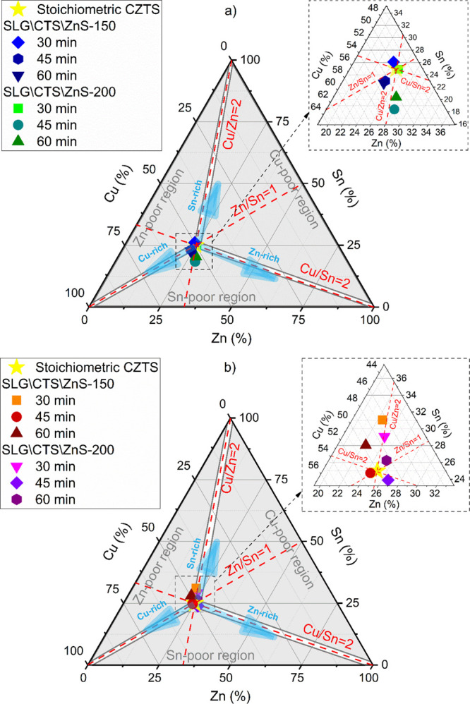
Ternary phase diagram showing the metallic elemental composition of the CZTS films annealed under (a) S and (b) Sn + S, atmospheres, for different durations, using two ZnS layer thicknesses.
Table 1. Chemical Elemental Composition (at %) of the SLG\CTS\ZnS-150 and SLG\CTS\ZnS-200 Annealed under an S Atmosphere for 30, 45, and 60 min.
| sample ID | annealing time (min) | Cu | Zn | Sn | S | Cu/Zn + Sn | Zn/Sn | S/metal | film stoichiometry |
|---|---|---|---|---|---|---|---|---|---|
| SLG\CTS\ZnS-150 | 30 | 25.58 | 12.37 | 13.39 | 48.66 | 0.99 | 0.92 | 0.95 | Cu2.05Zn0.99Sn1.07S3.89 |
| 45 | 31.21 | 14.53 | 13.67 | 40.59 | 1.17 | 1.06 | 0.63 | Cu2.65Zn1.16Sn1.09S3.24 | |
| 60 | 31.13 | 14.37 | 13.32 | 41.18 | 1.12 | 1.08 | 0.70 | Cu2.49Zn1.14Sn1.06S3.29 | |
| SLG\CTS\ZnS-200 | 30 | 24.85 | 12.68 | 12.45 | 50.02 | 0.99 | 1.02 | 1.00 | Cu1.99Zn1.01Sn1.00S4.00 |
| 45 | 31.47 | 16.47 | 10.81 | 41.25 | 1.15 | 1.52 | 0.70 | Cu2.51Zn1.31Sn0.86S3.30 | |
| 60 | 31.20 | 16.29 | 12.16 | 40.35 | 1.06 | 1.33 | 0.67 | Cu2.49Zn1.30Sn0.97S3.23 |
Figure 4b presents a ternary diagram with the metallic composition of SLG\CTS\ZnS-150 and SLG\CTS\ZnS-200 stacks annealed under the Sn + S atmosphere for 30, 45, and 60 min. For the first stack, with a 150 nm-thick ZnS layer, the film annealed for 30 min is slightly Sn-rich, while Cu and Zn contents are nearly stoichiometric. By increasing the annealing time to 45 and 60 min, the samples lost some SnS and became closer to the intended composition, especially the film annealed for 45 min. However, all three samples are slightly shifted toward the Sn-rich region. On the other hand, using a 200 nm ZnS layer and increasing the annealing time seems to help compensate the Sn surplus. The sample annealed for 30 min is slightly Sn-rich, but by increasing the annealing time SnS is lost and the two films annealed for 45 and 60 min get closer to the optimal CZTS stoichiometry. It is worth mentioning that almost all samples in both stacks are located in the Zn-poor region, which means that the probability of the coexistence of a ZnS secondary phase is very low because this phase is known to form in CZTS films with a Zn-rich composition.26Table 2 shows the chemical composition of the SLG\CTS\ZnS-150 and SLT\CTS\ZnS-200 stacks annealed for 30, 45, and 60 min. It can be seen that all the films are Sn-rich regardless of the annealing time or the ZnS thickness, making the Zn/Sn ratio < 1 in almost all films, and this is due to the Sn + S annealing atmosphere. The Cu/Zn + Sn ratio is close to 1 in all films, while the S/metal is slightly lower than 1, except for the SLG\CTS\ZnS-200 sample annealed for 60 min (Cu1.92Zn1.00Sn1.03S4.05), which is also the closest to the ideal stoichiometry (i.e., 2:1:1:4).
Table 2. Chemical Elemental Composition (at %) of the SLG\CTS\ZnS-150 and SLG\CTS\ZnS-200 Annealed under an Sn + S Atmosphere for 30, 45, and 60 min.
| sample reference | annealing time (min) | Cu | Zn | Sn | S | Cu/Zn + Sn | Zn/Sn | S/metal | film stoichiometry |
|---|---|---|---|---|---|---|---|---|---|
| SLG\CTS\ZnS-150 | 30 | 24.05 | 11.66 | 16.09 | 48.20 | 0.87 | 0.72 | 0.93 | Cu1.93Zn0.93Sn1.28S3.86 |
| 45 | 30.44 | 14.61 | 14.81 | 40.14 | 1.03 | 0.97 | 0.67 | Cu2.43Zn1.17Sn1.18S3.22 | |
| 60 | 27.09 | 12.15 | 15.30 | 45.46 | 0.98 | 0.79 | 0.83 | Cu2.16Zn0.97Sn1.22S3.65 | |
| SLG\CTS\ZnS-200 | 30 | 24.58 | 12.33 | 15.14 | 47.95 | 0.89 | 0.81 | 0.92 | Cu1.96Zn0.99Sn1.21S3.84 |
| 45 | 29.43 | 15.88 | 14.22 | 40.47 | 0.92 | 1.11 | 0.68 | Cu2.36Zn1.27Sn1.13S3.24 | |
| 60 | 23.87 | 12.49 | 12.92 | 50.72 | 0.94 | 0.97 | 1.03 | Cu1.92Zn1.00Sn1.03S4.05 |
Figure 5 shows the XPS data for the samples SLG\CTS\ZnS-200 annealed in the S atmosphere for 30 min and annealed in the Sn + S atmosphere for 60 min, as they are the closest to the ideal stoichiometry. High-resolution spectra for all the core levels of interest (Cu 2p, Zn 2p3/2, Sn 3d5/2, and S 2p) were acquired, as well as Cu LMM Auger transition for a better identification of the charge state for Cu, along with O 1s and C 1s. Prior to the measurement, the first layers of contaminants were removed with the help of Ar+ sputtering for 10 min at 3 keV energy and 10 mA current.
Figure 5.

High-resolution spectra for (a) Cu 2p, (b) Zn 2p3/2, (c) Sn 3d5/2, and (d) S 2p for the samples SLG\CTS\ZnS-200 sulfurized for 30 min represented with a blue marker, and for the sample SLG\CTS\ZnS-200 annealed in the Sn + S atmosphere for 60 min represented with a green marker. The black lines are the fit lines while the colored lines represent each individual component.
The surface signal as it comes from the integral amplitudes in XPS is 21.3% Cu, 16.4% Zn, 21.9% Sn, and 40.4% S in the case of SLG\CTS\ZnS-200 annealed for 30 min in the S atmosphere and 18.6% Cu, 14.7% Zn, 22.1% Sn, and 44.6% S in the case of SLG\CTS\ZnS-200 annealed for 60 min in the Sn + S atmosphere. The amplitudes were corrected by using the Wagner atomic sensitivity factors relative to F 1s.27 The surfaces are Zn and Sn rich in both cases, while they are deficient in Cu and in S. A possible explanation is the diffusion of Cu in the bulk and the preferential sputtering of S as it is the lightest species from the surface. The reason why Sn gives a higher signal is that its kinetic energy is much higher than that of Cu 2p and Zn 2p core levels, so Sn has a bigger inelastic mean free path. By taking into consideration all the factors that influence the XPS signal such as surface sensitivity, atoms migrating to the bulk or to the surface, and the overall depth of probing, which is at most 10 nm for elements with higher kinetic energy, it can be concluded that the composition as determined by EDS is more accurate.
Inspecting the Cu 2p spectra, it can be inferred that no Cu2+ remains on the surface after sputtering because no satellites are visible in the spectra. The main components represented with red have 932.4 eV binding energy and they are assigned to Cu1+.28 The assignment is also in agreement with the calculated modified Auger parameter for each component reported to the Cu LMM Auger transition: it has values of 1849.5 and 1849.9 for the sample SLG\CTS\ZnS-200 annealed in Sn + S for 60 min and 1849.8 for the sample SLG\CTS\ZnS-200 annealed in sulfur for 30 min.29 The secondary component in the SLG\CTS\ZnS-200 sulfurized in the 30 min Cu 2p spectrum is attributed to Cu0, having an Auger parameter of 1850.9.27
In both cases, Zn on the surface is more reactive, but the main component is Zn2+ having binding energies close to 1022 eV (±0.1 eV).30 The component at lower binding energies, 1021 eV, is attributed to Zn0, while the component at higher binding energies comes from surface defects and undercoordinated atoms. The Sn 3d spectrum has the main contribution coming from Sn4+ at 486.2 eV,30 and it also shows a small contribution coming from surface defects that only represents about 1% of the total Sn signal.
In the case of the S 2p spectrum, the main component at 161.5 eV is coming from S2– in the CZTS. One may observe that the etching is not removing all the SO3 and SO4 groups in neither case, while in the spectrum of the SLG\CTS\ZnS-200 sample annealed in the sulfur atmosphere for 30 min, there is also an additional component that we attributed to the ZnS phase on its surface.31
In Figure 6 are represented the GIXRD patterns of the SLG\CTS\ZnS-150 and SLG\CTS\ZnS-200 stacks annealed in S (Figure 6b) and Sn + S (Figure 6c) atmospheres for 30, 45, and 60 min. The ICDD PDF file that matches all the peaks in most of the diffractograms, namely, PDF 04-015-0223 for tetragonal Cu2ZnSnS4 is depicted in Figure 6a, showing that a tetragonal CZTS phase is formed in all the samples in a quantity of more than 95%.
Figure 6.

GIXRD results. (a) ICDD PDF 04-015-0223 of the tetragonal Cu2ZnSnS4 phase. The X-ray diffraction (XRD) patterns of the CZTS films, synthesized using a layer of ZnS, with a thickness of 150 and 200 nm, on top of a CTS layer, annealed for 30, 45, and 60 min in (b) sulfur and (c) tin + sulfur atmospheres. The 101 peak (I = 100) of the ZnS phase (hexagonal, P63mc (186), ICDD PDF 04-012-8144) is indicated with “*,” the 103 peak (I = 100) of the CuS phase (hexagonal, P63/mmc (194), ICDD PDF 04-008-8460) is indicated with “#,” and the 110 peak (I = 100) of the SnS2 phase (hexagonal, P63mc (186), ICDD PDF 00-021-1231) is indicated with “@.”
Table 3 shows the detailed ICDD PDF files for each sample together with the unit cell parameters (a and c). Several binary and ternary secondary phases can form during the synthesis of CZTS such as SnxSy, CuxS, CuxSnSy, and ZnS.17,18 As it can be seen in Table 3, in all 12 samples there are traces (less than 2.5%) of hexagonal ZnS, while in the samples annealed in the Sn + S atmosphere, additionally the hexagonal SnS2, also as traces (less than 2.5%), is formed. The presence of ZnS in very low quantities might be due to unreacted atoms from the top layer. The presence of the SnS2 secondary phase is due to the used Sn + S annealing atmosphere.32 In fact, the Sn + S annealing ambiance forms SnS vapor that reacts with the CTS and ZnS layers to form the CZTS phase. During the cooling process, the SnS vapors reoxidize and SnS2 is formed and condensates on the sample surfaces.33 On the other hand, the presence of a tetragonal CTS secondary phase cannot be excluded. The powder XRD patterns of the CTS, ZnS, and CZTS phases are very similar.34 Hence, Raman spectroscopy is needed as a complementary tool to further investigate the structural properties of the prepared samples and identify the possible presence of these secondary phases.
Table 3. Best ICDD PDF Files That Fit All the XRD Peaks of the Predominant Tetragonal CZTS Phase in Each Sample Synthesized by the Deposition of a ZnS Layer, with a Thickness of 150 and 200 nm, on Top of the CTS Layer, Annealed for 30, 45, and 60 min in Sulfur and Tin + Sulfur Atmospheres.
| sample and annealing atmosphere | annealing time (min) | predominant phase ratio, composition, ICDD PDF no., lattice system, space group, and a (Å)/c (Å) | secondary phases, ratio, composition, ICDD PDF no., lattice system, and space group | |
|---|---|---|---|---|
| SLG\CTS\ZnS-150, sulfur | 30 | 99%, Cu2.57Zn0.74Sn0.58S3.28, 04-024-9293, tetragonal, I-4 (82), 5.421/10.830 | 1%, ZnS, 04-012-8144, hexagonal, P63mc (186) | |
| 45 | 99%, Cu1.71Zn1.18Sn0.99S4, 04-023-6315, tetragonal, I-4 (82), 5.430/10.822 | 1%, ZnS, 04-012-8144, hexagonal, P63mc (186) | ||
| 60 | 99%, Cu1.71Zn1.18Sn0.99S4, 04-023-6315, tetragonal, I-4 (82), 5.430/10.822 | 1%, ZnS, 04-012-8144, hexagonal, P63mc (186) | ||
| SLG\CTS\ZnS-200, sulfur | 30 | 98%, Cu1.71Zn1.18Sn0.99S4, 04-023-6315, tetragonal, I-4 (82), 5.430/10.822 | 1%, ZnS, 04-012-8144, hexagonal, P63mc (186) | 1%, CuS, 04–008-8460, hexagonal, P63-mmc (194) |
| 45 | 99%, Cu1.88Zn1.06SnS4, 04-024-5532, tetragonal, I-4 (82), 5.434/10.834 | 1%, ZnS, 04-012-8144, hexagonal, P63mc (186) | ||
| 60 | 99%, Cu1.93Zn0.58Sn0.39S2.80, 04-024-9292, tetragonal, I-4 (82), 5.434/10.835 | 1%, ZnS, 04-012-8144, hexagonal, P63mc (186) | ||
| SLG\CTS\ZnS-150, tin + sulfur | 30 | 98%, Cu2ZnSnS4, 04-015-0223, tetragonal, I-42m (121), 5.428/10.864 | 1%, ZnS, 04-012-8144, hexagonal, P63mc (186) | 1%, SnS2, 00–021-1231, hexagonal, P63mc (186) |
| 45 | 98%, Cu2ZnSnS4, 01-083-4818, tetragonal, I-42m (121), 5.435/10.846 | 1%, ZnS, 04-012-8144, hexagonal, P63mc (186) | 1%, SnS2, 00–021-1231, hexagonal, P63mc (186) | |
| 60 | 98%, Cu2ZnSnS4, 04-015-0223, tetragonal, I-42m (121), 5.428/10.864 | 1%, ZnS, 04-012-8144, hexagonal, P63mc (186) | 1%, SnS2, 00–021-1231, hexagonal, P63mc (186) | |
| SLG\CTS\ZnS-200, tin + sulfur | 30 | 96%, Cu2ZnSnS4, 04-015-0223, tetragonal, I-42m (121), 5.428/10.864 | 2%, ZnS, 04-012-8144, hexagonal, P63mc (186) | 2%, SnS2, 00–021-1231, hexagonal, P63mc (186) |
| 45 | 97%, Cu2ZnSnS4, 04-015-0223, tetragonal, I-42m (121), 5.428/10.864 | 1.5%, ZnS, 04-012-8144, hexagonal, P63mc (186) | 1.5%, SnS2, 00–021-1231, hexagonal, P63mc (186) | |
| 60 | 95%, Cu2ZnSnS4, 04-015-0223, tetragonal, I-42m (121), 5.428/10.864 | 2.5%, ZnS, 04-012-8144, hexagonal, P63mc (186) | 2.5%, SnS2, 00–021-1231, hexagonal, P63mc (186) | |
The average CZTS crystallite size in each sample, presented in Table 4, was estimated using the Scherrer equation from the most intense peak, 112, taking into account the instrumental broadening.28 It ranges from 15 to 24 nm. The unit cell parameters (a and c) of the tetragonal CZTS phases calculated from the position of the 002, 110, 112, and 200 peaks for the six samples annealed in the S atmosphere and from the position of the 112 and 200 peaks for the other six films annealed in the Sn + S atmosphere are also shown.
Table 4. Average Crystallites Size (D) and the Unit Cell Parameters (a and c) of the Tetragonal CZTS Phase in the SLG\CTS\ZnS-150 and SLG\CTS\ZnS-200 Samples Annealed under S and Sn + S Atmospheres for 30, 45, and 60 min.
| sulfur
atmosphere |
tin
+ sulfur atmosphere |
|||||||||||
|---|---|---|---|---|---|---|---|---|---|---|---|---|
| SLG\CTS\ZnS-150 | SLG\CTS\ZnS-200 | SLG\CTS\ZnS-150 | SLG\CTS\ZnS-200 | |||||||||
| 30 min | 45 min | 60 min | 30 min | 45 min | 60 min | 30 min | 45 min | 60 min | 30 min | 45 min | 60 min | |
| D (nm) | 23 | 23 | 24 | 18 | 15 | 19 | 22 | 20 | 19 | 17 | 21 | 20 |
| a (Å) | 5.427 | 5.426 | 5.431 | 5.434 | 5.434 | 5.437 | 5.431 | 5.432 | 5.432 | 5.430 | 5.430 | 5.430 |
| c (Å) | 10.834 | 10.855 | 10.837 | 10.831 | 10.852 | 10.872 | 10.868 | 10.868 | 10.864 | 10.863 | 10.870 | 10.861 |
Determination of the average concentration of the elements inside the crystallites using only conventional XRD measurements is not possible. The chemical bonding between metals and sulfur in CZTS is covalent (directional)35 but has a strong ionic character;36 therefore, the positions of the Cu+ and Zn2+ cations (which have the same number of electrons) in the unit cell are not distinguishable by XRD.37 Therefore, to infer the quality of the CZTS networks (namely the ratio and the type of the antisite defects, vacancies, and deviations from stoichiometry) from the values of their unit cell parameters (a and c), in each of the 12 samples, and how they modify with the variation of the synthesis parameters (thickness of the ZnS layer, the annealing atmosphere, and time), accurate data of the CZTS structure were collected from scientific literature. The aim of this analysis was to see if there is any relation between the variation of a and c with the type and percent of defects present in the CZTS network. The data are synthetically presented in Table 5 and Figure 5. The term “partial disordered kesterite”38 is used for the CZTS network in which the copper and zinc atoms are randomly distributed on the 2c and 2d Wyckoff positions, while the 2a Wyckoff position is totally occupied by copper atoms (as in kesterite). Thus, the structure becomes more symmetric and belongs to the I-42m space group. Also, the data for tetrahedral Cu2.988Sn1.012S3.6 are presented, which in our analysis can be considered as a borderline case of a defective CZTS tetrahedral network.
Table 5. Accurate Structural Data for the CZTS Unit Cell Found in the Scientific Literaturea.
| accurate average composition of the CZTS crystal/powder/thin film | accurate average composition of the CZTS crystallites | crystal structure and space group | a (Å) | defects type on Wyckoff positions |
|---|---|---|---|---|
| c (Å) | ||||
| c/2a | ||||
| single crystal40 | Cu2ZnSnS4, PDF 00-026-0575 | stannite, I-42m (121) | 5.427 | |
| 10.848 | ||||
| 0.9994 | ||||
| Cu1.99ZnSn1.01S4 powder, quenched in ice water37 | Cu2ZnSnS4, PDF 04-015-0223 | partial disordered kesterite, I-42m (121) | 5.4282 | 50% ZnCu (4d) |
| 10.8644 | 50% CuZn (4d) | |||
| 1.0008 | ||||
| (41) Cu1.94Zn1.16Sn0.98S3.92 powder | Cu2ZnSnS4, PDF 04-017-3032 | kesterite, I-4 (82) | 5.4322 | 14% SnCu (2a) |
| 10.8434 | 14% CuSn (2b) | |||
| 0.9981 | ||||
| Cu1.98ZnSn1.05S3.96 single crystal, quenched in ice water35 | Cu2ZnSnS4, PDF 04-015-7542 | partial disordered kesterite, I-42m (121) | 5.434 | 50% ZnCu + 50% CuZn (4d) |
| 10.856 | ||||
| 0.9989 | ||||
| Cu1.996Zn1.001Sn1.008S4.000single crystal42 | Cu2ZnSnS4, PDF 01-080-8225 | kesterite, I-4 (82) | 5.4342 | 13.9% SnCu (2a) |
| 10.8496 | 13.9% CuSn (2b) | |||
| 0.9983 | ||||
| single crystal, quenched in ice water43 | Cu2ZnSnS4, PDF 01-083-4818 | partial disordered kesterite, I-42m (121) | 5.4353 | 50% ZnCu + 50% CuZn (4d) |
| 10.8464 | ||||
| 0.9978 | ||||
| Cu2.00Zn1.02Sn0.99S4.00 powder, cooling rate of 60 K/h44 | Cu2ZnSnS4 | partial disordered kesterite, I-4 (82) | 5.43547 | 28% ZnCu (2c) |
| 10.84438 | 28% CuZn (2d) | |||
| 0.9976 | ||||
| powder from thin film, cooling rate of 5 °C/min to 200 °C, then natural cooling45 | Cu1.969Zn1.19Sn0.841S4 | partial disordered kesterite, I-4 (82) | 5.4380 | 23% ZnCu (2a) |
| 10.857 | 4% CuZn (2d) | |||
| 0.9983 | 15.9% CuSn (2b) | |||
| (46) powder from thin film, cooling rate of 5 °C/min to 200 °C, then natural cooling | Cu2.18Zn1.143Sn0.677S4.00 | partial disordered kesterite, I-4 (82) | 5.4396 | 14.3% ZnCu (2a) |
| 10.8591 | 32.3% CuSn (2b) | |||
| 0.99815 | ||||
| powder from thin film, cooling rate of 5 °C/min to 200 °C, then natural cooling46 | Cu2.063Zn1.095Sn0.842S4.00 | partial disordered kesterite, I-4 (82) | 5.4412 | 36.1% ZnCu (2a) |
| 10.8640 | 26.6% CuZn (2d) | |||
| 0.9983 | 15.8% CuSn (2b) | |||
| powder, natural cooling38 | Cu2.572Zn0.738Sn0.58S3.28, PDF 04-024-9293 | partial disordered kesterite, I-4 (82) | 5.42072 | 8.7% ZnCu + 3% VCu (2a) |
| 10.83023 | 9.9% ZnCu + 1% VCu (2c) | |||
| 0.99897 | 54.9% CuZn + 7% VZn (2d) | |||
| 25% CuSn + 17% ZnSn (2b) | ||||
| 18% VS (8 g) | ||||
| Cu2.134Zn0.837Sn1.040S4.000 single crystal47 | Cu2.12Zn0.82Sn1.06S4 | kesterite, I-4 (82) | 5.42936 | 6% SnCu (2c) |
| 10.8391 | 18% CuZn (2d) | |||
| 0.9982 | ||||
| Cu1.711Zn1.181Sn0.994S4.000 single crystal47 | Cu1.674Zn1.163SnS4, PDF 04–023-6315 | kesterite, I-4 (82) | 5.43006 | 16.3% VCu (2a) |
| 10.8222 | 16.3% ZnCu (2c) | |||
| 0.9965 | ||||
| (42) Cu1.711Zn1.181Sn0.994S4.000 single crystal | Cu1.884Zn1.058SnS4, PDF 04-024-5532 | kesterite, I-4 (82) | 5.4344 | 5.8% VCu (2a) |
| 10.8337 | 5.8% ZnCu (2c) | |||
| 0.9935 | ||||
| powder from thin film, cooling rate of 5 °C/min to 200 °C, then natural cooling46 | Cu1.731Zn1.367Sn0.902S4 | partial disordered kesterite, I-4 (82) | 5.4424 | 38.5% ZnCu (2a) |
| 10.8620 | 50.2% ZnCu (2c) | |||
| 0.9979 | 52.0% CuZn (2d) | |||
| 9.8% CuSn (2b) | ||||
| powder, natural cooling38 | Cu1.933Zn0.577Sn0.39S2.8, PDF 04-024-9292 | partial disordered kesterite, I-4 (82) | 5.43442 | 36% VCu (2a) |
| 10.83451 | 30% VCu (2c) | |||
| 0.9968 | 12.3% CuZn + 44% VZn (2d) | |||
| 47% CuSn + 14% ZnSn (2b) | ||||
| 30% VS (8g) | ||||
| pellets, quenched in iced water48 | Cu2.988Sn1.012S3.6, PDF 04-020-3908 | I-42m (121) | 5.42247 | 48.2% Cu (2b) |
| 10.8259 | 24.1% Sn (4d) | |||
| 0.9982 | 10% VS (8g) |
The form of the investigated material (single crystal, powder, and thin film), the cooling rate at the end of the CZTS synthesis process, and the ICDD PDF numbers where the same data are reported are also given.
It can be seen (Table 5) that obtaining a stoichiometric CZTS network in the pure form of kesterite (space group I-4 (82)) without any defects is difficult (no scientific article was found). Also, the nonstoichiometric CZTS networks could be more or less disordered. This is due to the tetrahedral bonds (to obtain the diffusion of Zn, Cu, and Sn atoms, from the wrong positions to the correct ones, four bonds must be broken, via an interstitial mechanism,36 or two bonds, via topological modifications39), the sulfur volatility (which creates sulfur vacancies), the cation vacancies, the disordered distribution of the cations (antisite defects), and even the presence of cations in the network interstices (aspect that has not been taken into account so far in the fitting of experimental diffraction data38).
Another conclusion revealed by analyzing the data in Table 5 is that there is a difference between the concentration of the elements in the entire material (thin film, powder, and single crystal) and the concentration of the elements in the unit cell. This difference will be higher when the average crystallite size is nanometric, because the number of atoms at the grain boundaries represents a significant percentage in relation to the number of atoms inside the crystallites. Therefore, the correlation between the concentration of the elements in the entire material and the structure and properties of that material with nanometric crystallites is affected by large errors.
In Figure 7a,b is presented the variation of the unit cell parameters (a and c/2, values taken from the Table 4) of the tetragonal CZTS phases with the annealing time (for all 12 samples), while in Figure 7c,d is shown the variation of the unit cell parameters (a and c/2, from values taken Table 5) with the average disorder per Wyckoff position (the sum of all defect ratios in the unit cell, divided by 8). The length of the chemical bonds between metals (Me) and sulfur is Cu–S: 2.330–2.333 Å (in kesterite),35,49 2.307 Å (in Cu2.665Sn1.335S4);50 Zn–S: 2.342 Å (in sphalerite);49 Sn–S: 2.408–2.409 Å (in kesterite)35,49 and 2.416 Å (in Cu2.665Sn1.335S4).50
Figure 7.

Unit cell parameters (a and c/2) of the tetragonal CZTS phases in the SLG\CTS\ZnS-150 and SLG\CTS\ZnS-200 samples annealed in (a) S and (b) Sn + S atmospheres for 30, 45, and 60 min. The variation of the unit cell parameters (c) a and (d) c/2, with the mean disorder per Wyckoff position (the sum of the ratio of all defects in the unit cell, divided by 8) obtained from accurate structural data found in the scientific literature (Table 5).
Therefore, there are significant differences in Me–S bond lengths, while the deviation from the stoichiometry and the point defects should influence the values of a and c. We can make the following observations: (i) if the value of the a parameter is bigger than 5.437 Å and the value of the c/2 parameter is bigger than 5.428 Å, then, most probably, the CZTS network is nonstoichiometric, the ratio of Sn is ≤1 and the average antisite defect per Wyckoff position is at least 5.3%; (ii) if the value of the c/2 parameter is smaller than 5.418 Å, whatever the value of the a parameter, then, most probably, the CZTS network is nonstoichiometric and there are antisite defects and voids.
Regarding our samples, the following assessments can be made: (i) for the samples annealed in the sulfur atmosphere the SLG\CTS\ZnS-150 and SLG\CTS\ZnS-200 films annealed for 45 min contain only antisite defects in the unit cell; the other films have the values of the a parameter higher than 5.437 Å (1 sample) or the values of the c parameter lower than 5.419 Å (3 samples); (ii) all the samples annealed in the Sn + S atmosphere have only antisite defects in the unit cell.
Raman spectra, of the CZTS films annealed under an S atmosphere for 30, 45, and 60 min, using different excitation wavelengths (the upper panels use λ = 325 nm and the bottom panels λ = 633 nm) are represented in Figure 8, with the SLG\CTS\ZnS-150 stack illustrated in Figure 6a and the SLG\CTS\ZnS-200 stack in Figure 8b. The four peaks at 288, 337, 365, and 374 cm–1, observed in the spectra, for 633 nm excitation wavelength, of both stacks annealed under an S atmosphere for different periods, belong to the CZTS phase. A small shoulder at 327 cm–1 is observed in the SLG\CTS\ZnS-150 stack (633 nm), which can be attributed to the A mode of bulk CZTS. The main reason behind this shift from the 337 cm–1 CZTS characteristic peak is due to a disorder in the Cu–Zn layer.51,52 No other peaks related to secondary phases were detected. On the other hand, it is known that the ZnS phase resonates at around 350 cm–1 under a 325 nm excitation wavelength in Raman spectra.53,54 Two main peaks were observed in both stacks regardless of the annealing time. The most intense peak at 337 cm–1 is attributed to the CZTS kesterite phase, while the second Raman mode at 347/348 cm–1 can be assigned either to the CZTS or ZnS secondary phase,55,56 as also observed in GIXRD.
Figure 8.

Raman spectra of CZTS films prepared with (a) 150 nm and (b) 200 nm of the ZnS top layer and annealed in the S atmosphere for 30, 45, and 60 min using two different excitation wavelengths (325 and 633 nm). On the right side are shown the relative optical images with the measured spot for each sample.
Figure 9 presents the experimental Raman spectra of the CZTS films annealed in the Sn + S atmosphere for 30, 45, and 60 min and measured under 325 and 633 nm excitation wavelengths, with the 150 and 200 nm-thick ZnS top layer samples being shown in Figure 9a and Figure 9b, respectively. By analyzing the bottom panels, the strong peak at 337 cm–1 is related to the A symmetry assigned to S atom vibration in CZTS. The less intense peak at 288 cm–1 is due to A symmetry characteristic of the Cu, Zn, and S atom vibrations in CZTS. The two other CZTS peaks at 365 and 374 cm–1 are related to E and B symmetries, respectively.57 In addition, the SnS2 secondary phase, observed in GIXRD, is also detected by Raman spectroscopy in almost all the samples with a peak at 320 cm–1.58 The reason why SnS2 was not detected in the SLG\CTS\ZnS-200 sample, annealed for 30 min, can be explained by the detection limits of Raman spectroscopy which is a surface-sensitive analysis technique. Also, the contrast in the image does not allow to distinguish those SnS2 large grains, and thus Raman spectroscopy was performed on random clusters. The strong peak at 337 cm–1 in the top panels confirms also the formation of the CZTS phase in all the films. In addition, a second Raman mode at 347 cm–1 is also observed in all samples. This peak was identified by Dimitrievxska et al.,57 Guc et al.,55 and Schorr et al.59 as the E symmetry mode of the CZTS phase. However, other studies suggest that this peak is related to the ZnS secondary phase,21,60 which was also identified by GIXRD, which can be due to the excess of this phase resulting from the thick ZnS top layer or due to the segregation of some unreacted particles within the CTS layer.
Figure 9.

Raman spectra of CZTS films prepared with (a) 150 nm and (b) 200 nm of the ZnS top layer and annealed in the Sn + S atmosphere for 30, 45, and 60 min using two different excitation wavelengths (325 and 633 nm). On the right side are shown the relative optical images with the measured spot for each sample.
Figure 10 represents the Tauc plots of the two stacks annealed in the S atmosphere for 30, 45, and 60 min. The optical band gap energies were inferred from transmittance data and estimated using the following equations:4
| 1 |
| 2 |
where α is the absorption coefficient, E is the photon energy, A is the constant of proportionality, d is the film thickness, Eg is the optical band gap, T is the transmittance, and Abs is the absorbance. The Eg was determined using the Tauc plot by representing (Abs × E)2 vs E near the absorption edge. The optical band gaps for the CZTS stack with a 150 nm ZnS top layer and annealed for 30, 45, and 60 min (Figure 8a) are 1.42, 1.49, and 1.48 eV, respectively. On the other hand, for the SLG\CTS\ZnS-200 stack in Figure 8b, the optical band gaps are 1.47, 1.46, and 1.50 eV, respectively. All the computed values are in agreement with the reported CZTS band gap (1.40–1.50 eV).61
Figure 10.

Tauc plots of the CZTS films annealed under the S atmosphere for 30, 45, and 60 min with (a) samples prepared using a 150 nm ZnS top layer and (b) samples prepared using a 200 nm ZnS top layer.
In Figure 11 are illustrated the Tauc plots of the SLG\CTS\ZnS-150 and SLG\CTS\ZnS-200 stacks, respectively, annealed under the Sn + S atmosphere for 30, 45, and 60 min. The optical band gaps of the CZTS films, obtained from 150 nm ZnS-based film annealed for 30, 45, and 60 min, are 1.45, 1.38, and 1.46 eV, respectively. Regarding the stack with a 200 nm ZnS layer, the Eg values are 1.49, 1.43, and 1.47 eV, for the samples thermally treated for 30, 45, and 60 min, respectively. The fluctuations noticed in the computed band gaps might be due to the different elemental compositions of the films.62 However, these experimental Eg values are in the range of the ideal absorber layer band gap for high-efficiency solar cells.63 One should note that the optical band gap of all films does not seem to be affected by the presence of the SnS2 secondary phase observed in all samples, which may increase the value of the CZTS films due to its large band gap (≈2.2 eV).33 This confirms that SnS2 is present in a small amount in the samples.
Figure 11.

Tauc plots of the CZTS films annealed under the Sn + S atmosphere for 30, 45, and 60 min with (a) samples prepared using a 150 nm ZnS top layer and (b) samples prepared using a 200 nm ZnS top layer.
Hall measurement results obtained at room temperature are reported in Table 6. Before Hall measurement, molybdenum electrodes were deposited on CZTS films. In this way, the ohmic contact between electrodes and CZTS films was ensured. The measurements were performed by sweeping the magnetic field in the range of −2 ÷ 2 Tesla using the van der Pauw configuration. For all samples, p-type conductivity behavior was recorded.
Table 6. Hall Effect Measurement Results Obtained at Room Temperature.
| sample reference | annealing time (min) | conductivity | resistivity at 25 °C (Ω m) | carrier concentration (cm–3) | mobility (cm2 V–1 s–1) |
|---|---|---|---|---|---|
| SLG\CTS\ZnS-150, sulfur | 30 | p | 0.013 | 2.45 × 10¹⁸ | 1.91 |
| 45 | 0.001 | 9.65 × 10¹⁹ | 0.62 | ||
| 60 | 4.97 × 10⁻⁴ | 2.13 × 10²⁰ | 0.58 | ||
| SLG\CTS\ZnS-200, sulfur | 30 | p | 5.70 × 10⁻⁴ | 1.26 × 10²⁰ | 0.86 |
| 45 | 0.059 | 1.09 × 10¹⁸ | 0.96 | ||
| 60 | 0.082 | 3.15 × 10¹⁷ | 2.39 | ||
| SLG\CTS\ZnS-150, tin + sulfur | 30 | p | 0.074 | 3.48 × 10¹⁷ | 2.39 |
| 45 | 0.048 | 1.25 × 10¹⁸ | 1.03 | ||
| 60 | 0.081 | 8.57 × 10¹⁶ | 8.98 | ||
| SLG\CTS\ZnS-200, tin + sulfur | 30 | p | 0.37 | 3.17 × 10¹⁶ | 5.23 |
| 45 | 3.34 | 8.36 × 10¹⁵ | 2.23 | ||
| 60 | 0.18 | 5.34 × 10¹⁷ | 0.64 |
Compared with current state of the art,64−68 the obtained carrier concentration of our CZTS films is comparable or even higher (1015–1020 cm–3). These results provide further evidence that by choosing appropriate CZTS preparation/annealing conditions the carrier concentration and mobility can be tuned toward desired values.
4. Discussion
CZTS thin films were synthesized by a two-step magnetron sputtering deposition from stacked SLG\CTS\ZnS films with two different (150 and 200 nm) ZnS thicknesses and annealed in Sn + S and S atmospheres. The CTS bottom layer was prepared using two different stacks: a Cu deposit on top of a SnS2 layer and a SnS2 layer on top of Cu. Although the CuS phase was observed in all the CTS films, the Cu2SnS3 films used in this study contain less than 5% of this secondary phase.23 The SnS2-capped films showed the existence of voids and cavities at the surface which was due to the evaporation of the very volatile SnS during the annealing process.69 The surface morphology of the Cu-capped films was compact and homogeneous. Also, the composition of the CTS films was very close to the stoichiometry, with few films being slightly rich in Cu and Sn. For that reason, a Sn + S annealing atmosphere was employed to allow the Cu surplus to react with the SnS vapors and form more of the Cu2SnS3 phase70 and to further react with the ZnS upper layer.71 The addition of a ZnS layer in two different thicknesses was performed to provide a sufficient amount of ZnS to react with the CTS bottom layer. The reaction between CTS and ZnS is known to be the final step for the CZTS phase formation regardless of the starting films.72 However, an excess of ZnS phase segregated at the surface can be detrimental to CZTS-based solar cells because it can lower the grain size and cause short-circuit current which can decrease the efficiency.26 On the contrary, control of the ZnS amount and cluster size can help reduce the heterojunction interface recombination rate and thus improve the open-circuit voltage which can increase the CZTS solar PCE.26 In our case, the quantity of the ZnS secondary phase is as low as 1–2.5% in the films, regardless of the annealing time or atmosphere, while the ZnS clusters were mainly located in the upper part of the samples (as observed by XPS measurements). On the other hand, the SnS2 secondary phase is also known to degrade the CZTS solar cells and was only detected in the samples annealed under Sn + S conditions. This shows that using the Sn and S atmosphere can help eliminate of the CuS secondary phase. This phase was previously observed in the CTS first film, but after the addition of ZnS and the annealing in Sn + S, CuS was never detected afterward in the CZTS final films. Furthermore, the Sn + S atmosphere can also be used to compensate for the SnS loss and reach stoichiometric amounts of Sn.73 However, the CTS films used here were Sn stoichiometric or slightly rich; thus the Sn + S annealing conditions led to a saturation of tin in the final samples, hence the apparition of the SnS2 secondary phase. This demonstrates that annealing under the S atmosphere is enough if the CTS film is Sn stoichiometric. Also, the sequential deposition process showed a homogeneous surface morphology with 1–2 μm large grains, which are beneficial to high-efficiency CZTS solar cells.74 The reason behind the large particles obtained is the two annealing processes, because the first heat treatment was performed to obtain the CTS layer, and then a second annealing was performed after the ZnS was deposited on top of CTS. Several studies suggest the need for a preannealing followed by a sulfurization to obtain large CZTS grains.75 Additionally, the CTS films prepared with SnS2 on top were characterized by voids which were totally covered by the ZnS top layer. The elemental compositions in all the 12 films were close to the ideal stoichiometry regardless of the annealing time or atmosphere. However, the use of two different ZnS thicknesses and annealing atmospheres makes it possible to control the composition. Annealing for 45 min under S conditions and using a 200 nm-thick ZnS top layer lead to stoichiometric samples with slightly Zn-rich CZTS films, which are preferred over the Sn-rich CZTS films obtained under the Sn + S atmosphere, for high-PCE solar cells.76 The optical band gap of all the samples is close to optimal values (1.4–1.5 eV) and seems not to be affected by the 50 nm difference in ZnS thickness, or the annealing atmosphere and duration.
5. Conclusions
In summary, CZTS films have been successfully synthesized by a sequential magnetron sputtering process from CTS\ZnS stacked films. The influence on the composition, morphology, atomic structure, chemical bonding, the optical, and electrical properties with annealing atmosphere (S or Sn + S) and time along with the thickness of the ZnS top layer was investigated. These steps show the ability to produce highly crystalline films very close to the single-phase CZTS. SnS2 and ZnS secondary phases were observed only in very low percentages by XRD and Raman in the samples. The morphology of the samples is characterized by a homogeneous surface with large particles. The EDX measurements showed that all the films are nearly stoichiometric, with the samples annealed in Sn + S slightly rich in Sn and the ones annealed in the S atmosphere slightly Zn-rich. XPS results showed a high concentration of zinc and tin, while low contents of copper and sulfur were observed at the surface of the films. All the band gap values were between 1.38 and 1.50 eV which is ideal for absorber layers. The Hall measurements revealed that all the films are p-type with a carrier concentration between 1015 and 1020 cm–3 and a mobility between 0.6 and 9 cm2/Vs. This new synthesis method can be regarded as a solution for obtaining high-quality CZTS films and can be applied in large-scale production.
Acknowledgments
The authors kindly acknowledge the financial support of the Romanian Ministry of Research, Innovation and Digitalization in the framework of the PN-III-P4-ID-PCE-2020-0827 (contract no. PCE74/09.02.2021) and PN-III-P1-1.1-PD-2021-0240 (contract no. PD 41/2022) projects and Core Program PN19-03 (contract no. 21N/08.02.2019). The fee for open access publication was supported from the project 35PFE/2021, funded by the Romanian Ministry of Research, Innovation and Digitization.
The authors declare no competing financial interest.
References
- Wang Z.; Demopoulos G. P. Nanoscale Photo-Absorbing Kesterite Grown on Anatase Mesoscopic Films by Sequential Binary Chalcogenide Solution Deposition-Exchange, Annealing, and Etching. Cryst. Growth Des. 2016, 16, 3618–3630. 10.1021/acs.cgd.6b00033. [DOI] [Google Scholar]
- Yu K.; Carter E. A. A Strategy to Stabilize Kesterite CZTS for High-Performance Solar Cells. Chem. Mater. 2015, 27, 2920–2927. 10.1021/acs.chemmater.5b00172. [DOI] [Google Scholar]
- Azmi S.; Moujib A.; Layachi O. A.; Matei E.; Galca A. C.; Zaki M. Y.; Secu M.; Rusu M. I.; Grigorescu C. E. A.; Khoumri E. M. Towards Phase Pure Kesterite Cu2ZnSnS4 Absorber Layers Growth via Single Step Free Sulfurization Electrodeposition under a Fix Applied Potential on Mo Substrate. J. Alloys Compd. 2020, 842, 155821 10.1016/j.jallcom.2020.155821. [DOI] [Google Scholar]
- El Khouja O.; Galca A. C.; Zaki M. Y.; Talbi A.; Ahmoum H.; Nouneh K.; Ebn Touhami M.; Taibi M.; Matei E.; Enculescu M.; Pintilie L. Secondary Phases and Their Influence on Optical and Electrical Properties of Electrodeposited Cu2FeSnS4 Films. Appl. Phys. A: Mater. Sci. Process. 2021, 127, 887. 10.1007/s00339-021-05038-y. [DOI] [Google Scholar]
- Chesman A. S. R.; van Embden J.; Duffy N. W.; Webster N. A. S.; Jasieniak J. J. In Situ Formation of Reactive Sulfide Precursors in the One-Pot, Multigram Synthesis of Cu2ZnSnS4 Nanocrystals. Cryst. Growth Des. 2013, 13, 1712–1720. 10.1021/cg4000268. [DOI] [Google Scholar]
- Huang T. J.; Lee Guang-Ren R.; Yin X.; Tang C.; Qi G.; Gong H. Effect of Sulfide Precursor Selection on the Nucleation, Growth, and Elemental Composition of Cu2ZnSnS4 Nanocrystals. Cryst. Growth Des. 2017, 17, 73–79. 10.1021/acs.cgd.6b01217. [DOI] [Google Scholar]
- Azmi S.; Khoumri E. M.; Marrakchi M. E.; Pezzato L.; Nohair M.; Dabala M. Structural and Optical Annealing Route-Dependent Properties of CZTS Thin Films Grown by One-Step Electrodeposition with Free Annealing Sulfurization for Photovoltaic Application. J. Electron. Mater. 2019, 48, 8254–8260. 10.1007/s11664-019-07677-7. [DOI] [Google Scholar]
- Ahmoum H.; Chelvanathan P.; Su’ait M. S.; Boughrara M.; Li G.; Al-Waeli A. H. A.; Sopian K.; Kerouad M.; Amin N. Impact of Preheating Environment on Microstructural and Optoelectronic Properties of Cu2ZnSnS4 (CZTS) Thin Films Deposited by Spin-Coating. Superlattices Microstruct. 2020, 140, 106452 10.1016/j.spmi.2020.106452. [DOI] [Google Scholar]
- Jeganath K.; Raviprakash Y. Near-Optimal Composition of CZTS Thin Film via Exploration of Copper and Thiourea Molar Concentration in Spray Pyrolysis Technique. Mater. Res. Express 2021, 8, 116404. 10.1088/2053-1591/ac343e. [DOI] [Google Scholar]
- Varadharajaperumal S.; Sripan C.; Ganesan R.; Hegde G.; Satyanarayana M. N. Morphology Controlled N-Type TiO2 and Stoichiometry Adjusted p-Type Cu2ZnSnS4 Thin Films for Photovoltaic Applications. Cryst. Growth Des. 2017, 17, 5154–5162. 10.1021/acs.cgd.7b00632. [DOI] [Google Scholar]
- Whittles T. J.Electronic Characterisation of Earth-Abundant Sulphides for Solar Photovoltaics; Springer Theses; Springer International Publishing, 2018. [Google Scholar]
- Olgar M. A.; Klaer J.; Mainz R.; Ozyuzer L.; Unold T. Cu2ZnSnS4-Based Thin Films and Solar Cells by Rapid Thermal Annealing Processing. Thin Solid Films 2017, 628, 1–6. 10.1016/j.tsf.2017.03.008. [DOI] [Google Scholar]
- Zaki M.-Y.; Sava F.; Buruiana A.-T.; Simandan I.-D.; Becherescu N.; Galca A.-C.; Mihai C.; Velea A. Synthesis and Characterization of Cu2ZnSnS4 Thin Films Obtained by Combined Magnetron Sputtering and Pulsed Laser Deposition. Nanomaterials 2021, 11, 2403. 10.3390/nano11092403. [DOI] [PMC free article] [PubMed] [Google Scholar]
- Xie M.; Zhuang D.; Zhao M.; Zhuang Z.; Ouyang L.; Li X.; Song J. Preparation and Characterization of Cu2ZnSnS4 Thin Films and Solar Cells Fabricated from Quaternary Cu-Zn-Sn-S Target. Int. J. Photoenergy 2013, 2013, 1–9. 10.1155/2013/929454. [DOI] [Google Scholar]
- Rudisch K.; Davydova A.; Riekehr L.; Adolfsson J.; Quaglia Casal L.; Platzer-Björkman C.; Scragg J. Prospects for Defect Engineering in Cu2ZnSnS4 Solar Absorber Films. J. Mater. Chem. A 2020, 8, 15864–15874. 10.1039/D0TA02598D. [DOI] [Google Scholar]
- Shi X.; Wang Y.; Yu H.; Wang G.; Huang L.; Pan D. Significantly Improving the Crystal Growth of a Cu2ZnSn(S,Se) 4 Absorber Layer by Air-Annealing a Cu2ZnSnS4 Precursor Thin Film. ACS Appl. Mater. Interfaces 2020, 12, 41590–41595. 10.1021/acsami.0c12630. [DOI] [PubMed] [Google Scholar]
- El Khouja O.; Negrila C. C.; Nouneh K.; Secu M.; Touhami M. E.; Matei E.; Stancu V.; Enculescu M.; Kuncser V.; Galca A. C. Bulk and Surface Characteristics of Co-Electrodeposited Cu2FeSnS4 Thin Films Sulfurized at Different Annealing Temperatures. J. Alloys Compd. 2022, 906, 164379 10.1016/j.jallcom.2022.164379. [DOI] [Google Scholar]
- Yarur Villanueva F.; Green P. B.; Qiu C.; Ullah S. R.; Buenviaje K.; Howe J. Y.; Majewski M. B.; Wilson M. W. B. Binary Cu2– x S Templates Direct the Formation of Quaternary Cu2ZnSnS4 (Kesterite, Wurtzite) Nanocrystals. ACS Nano 2021, 15, 18085–18099. 10.1021/acsnano.1c06730. [DOI] [PubMed] [Google Scholar]
- Li W.; Han X.; Zhao Y.; Liu L.; Wang J.; Yang S.; Tanaka T. Cu2ZnSnS4 Alloys Synthesized from Cu2SnS3@ZnS Nanoparticles via a Facile Hydrothermal Approach. Mater. Lett. 2014, 125, 167–170. 10.1016/j.matlet.2014.03.159. [DOI] [Google Scholar]
- Nagamalleswari D.; Kishore Kumar Y. B.; Kiran Y. B.; Suresh Babu G. Preparation and Characterization of Cu2ZnSnS4 Thin Films by Two-Stage Process. Energy Sources, Part A 2019, 41, 3001–3012. 10.1080/15567036.2019.1583294. [DOI] [Google Scholar]
- Gordillo G.; Becerra R.; Calderón C. Novel Chemical Route for Deposition of Cu2ZnSnS4 Photovoltaic Absorbers. J. Braz. Chem. Soc. 2018, 29, 649–658. 10.21577/0103-5053.20170179. [DOI] [Google Scholar]
- Park J.; Song M.; Jung W. M.; Lee W. Y.; Kim H.; Kim Y.; Hwang C.; Shim I.-W. Syntheses of Cu2SnS3 and Cu2ZnSnS4 Nanoparticles with Tunable Zn/Sn Ratios under Multibubble Sonoluminescence Conditions. Dalton Trans. 2013, 42, 10545. 10.1039/c3dt50849h. [DOI] [PubMed] [Google Scholar]
- Zaki M. Y.; Sava F.; Simandan I. D.; Buruiana A. T.; Mihai C.; Velea A.; Galca A. C. Effect of the Stacking Order, Annealing Temperature and Atmosphere on Crystal Phase and Optical Properties of Cu2SnS3. Sci. Rep. 2022, 12, 7958. 10.1038/s41598-022-12045-3. [DOI] [PMC free article] [PubMed] [Google Scholar]
- Lv X.; Zhu C.; Yang Y.; Liu R.; Fan W.; Wang Y. Performance Improvement of Cu2ZnSn(S,Se)4 Thin-Film Solar Cells by Optimizing the Selenization Temperature. AIP Adv. 2021, 11, 075205 10.1063/5.0053633. [DOI] [Google Scholar]
- Sawant J. P.; Pathan H. M. Photoelectrochemical Properties of Spray Deposited Cu2ZnSnS4 Photoelectrode: Enhancement in Photoconversion Efficiency with Film Thickness. ES Energy Environ. 2020, 10, 73–79. 10.30919/esee8c933. [DOI] [Google Scholar]
- Li W.; Chen J.; Yan C.; Hao X. The Effect of ZnS Segregation on Zn-Rich CZTS Thin Film Solar Cells. J. Alloys Compd. 2015, 632, 178–184. 10.1016/j.jallcom.2015.01.205. [DOI] [Google Scholar]
- Briggs D.Handbook of X-Ray Photoelectron Spectroscopy C. D. Wanger, W. M. Riggs, L. E. Davis, J. F. Moulder and G. E.Muilenberg Perkin-Elmer Corp., Physical Electronics Division, Eden Prairie, Minnesota, USA, 1979. 190 Pp. $195. Surf. Interface Anal. 1981, 3 (), 10.1002/sia.740030412. [DOI] [Google Scholar]
- Zaki M. Y.; Nouneh K.; Touhami M. E.; Matei E.; Badica P.; Burdusel M.; Negrila C. C.; Baibarac M.; Pintilie L.; Galca A. C. Influence of Boric Acid Concentration on the Properties of Electrodeposited CZTS Absorber Layers. Phys. Scr. 2020, 95, 054001 10.1088/1402-4896/ab6afd. [DOI] [Google Scholar]
- Niemi E.; Stolt L. Characterization of CuInSe2 Thin Films by XPS. Surf. Interface Anal. 1990, 15, 422–426. 10.1002/sia.740150705. [DOI] [Google Scholar]
- Ren Y.; Scragg J. J. S.; Edoff M.; Larsen J. K.; Platzer-Björkman C. Evolution of Na—S(—O) Compounds on the Cu2ZnSnS4 Absorber Surface and Their Effects on CdS Thin Film Growth. ACS Appl. Mater. Interfaces 2016, 8, 18600–18607. 10.1021/acsami.6b04978. [DOI] [PubMed] [Google Scholar]
- Barreca D.; Gasparotto A.; Maragno C.; Tondello E.; Spalding T. R. Analysis of Nanocrystalline ZnS Thin Films by XPS. Surf. Sci. Spectra 2021, 9, 54. 10.1116/11.20030117. [DOI] [Google Scholar]
- Turkoglu F.; Koseoglu H.; Cantas A.; Akca F. G.; Meric E.; Buldu D. G.; Ozdemir M.; Tarhan E.; Ozyuzer L.; Aygun G. Effect of Defects and Secondary Phases in Cu2ZnSnS4 Absorber Material on the Performance of Zn(O,S) Buffered Devices. Thin Solid Films 2019, 670, 6–16. 10.1016/j.tsf.2018.12.001. [DOI] [Google Scholar]
- Wang W.; Chen G.; Cai H.; Chen B.; Yao L.; Yang M.; Chen S.; Huang Z. The Effects of SnS2 Secondary Phases on Cu2ZnSnS4 Solar Cells: A Promising Mechanical Exfoliation Method for Its Removal. J. Mater. Chem. A 2018, 6, 2995–3004. 10.1039/C7TA08242H. [DOI] [Google Scholar]
- Zaki M. Y.; Nouneh K.; Ebn Touhami M.; Belakhmima R. A.; Galca A. C.; Pintilie L.; Enculescu M.; Baibarac M.; Taibi M. Effect of Mixing Complexing Agents on the Properties of Electrodeposited CZTS Thin Films. Opt. Mater. 2018, 83, 252–256. 10.1016/j.optmat.2018.06.030. [DOI] [Google Scholar]
- Bonazzi P.; Bindi L.; Bernardini G. P.; Menchetti S. A Model for the Mechanism of Incorporation of Cu, Fe and Zn in the Stannite – Kësterite Series, Cu2FeSnS4 – Cu2ZnSnS4. Can. Mineral. 2003, 41, 639–647. 10.2113/gscanmin.41.3.639. [DOI] [Google Scholar]
- Vaughan D. J.; Rosso K. M. Chemical Bonding in Sulfide Minerals. Rev. Mineral. Geochem. 2006, 61, 231–264. 10.2138/rmg.2006.61.5. [DOI] [Google Scholar]
- Schorr S.; Hoebler H.-J.; Tovar M. A Neutron Diffraction Study of the Stannite-Kesterite Solid Solution Series. ejm 2007, 19, 65–73. 10.1127/0935-1221/2007/0019-0065. [DOI] [Google Scholar]
- Bosson C. J.; Birch M. T.; Halliday D. P.; Tang C. C.; Kleppe A. K.; Hatton P. D. Polymorphism in Cu2ZnSnS4 and New Off-Stoichiometric Crystal Structure Types. Chem. Mater. 2017, 29, 9829–9839. 10.1021/acs.chemmater.7b04010. [DOI] [Google Scholar]
- Sava F. Characterization of the Interstitial Voids in the Structural Model of Amorphous Silicon Derived from the Diamond-Like Lattice. J. Optoelectron. Adv. Mater. 2003, 5, 1075–1080. [Google Scholar]
- Schäfer W.; Nitsche R. Tetrahedral Quaternary Chalcogenides of the Type Cu2-II-IV-S4(Se4). Mater. Res. Bull. 1974, 9, 645–654. 10.1016/0025-5408(74)90135-4. [DOI] [Google Scholar]
- Fischereder A.; Rath T.; Haas W.; Amenitsch H. Investigation of Cu2ZnSnS4 Formation from Metal Salts and Thioacetamide. Chem. Mater. 2010, 22, 3399–3406. 10.1021/cm100058q. [DOI] [Google Scholar]
- Choubrac L.; Lafond A.; Guillot-Deudon C.; Moëlo Y.; Jobic S. Structure Flexibility of the Cu2ZnSnS4 Absorber in Low-Cost Photovoltaic Cells: From the Stoichiometric to the Copper-Poor Compounds. Inorg. Chem. 2012, 51, 3346–3348. 10.1021/ic202569q. [DOI] [PubMed] [Google Scholar]
- Lafond A.; Choubrac L.; Guillot-Deudon C.; Fertey P.; Evain M.; Jobic S. X-Ray Resonant Single-Crystal Diffraction Technique, a Powerful Tool to Investigate the Kesterite Structure of the Photovoltaic Cu2ZnSnS4 Compound. Acta Crystallogr., Sect. B: Struct. Sci., Cryst. Eng. Mater. 2014, 70, 390–394. 10.1107/S2052520614003138. [DOI] [PubMed] [Google Scholar]
- Ritscher A.; Just J.; Dolotko O.; Schorr S.; Lerch M. A mechanochemical route to single phase Cu2ZnSnS4 powder. J. Alloys Compd. 2016, 670, 289–296. 10.1016/j.jallcom.2016.02.058. [DOI] [Google Scholar]
- Nozaki H.; Fukano T.; Ohta S.; Seno Y.; Katagiri H.; Jimbo K. Crystal Structure Determination of Solar Cell Materials: Cu2ZnSnS4 Thin Films Using X-Ray Anomalous Dispersion. J. Alloys Compd. 2012, 524, 22–25. 10.1016/j.jallcom.2012.01.134. [DOI] [Google Scholar]
- Washio T.; Nozaki H.; Fukano T.; Motohiro T.; Jimbo K.; Katagiri H. Analysis of Lattice Site Occupancy in Kesterite Structure of Cu2ZnSnS4 Films Using Synchrotron Radiation X-Ray Diffraction. J. Appl. Phys. 2011, 110, 074511 10.1063/1.3642993. [DOI] [Google Scholar]
- Lafond A.; Choubrac L.; Guillot-Deudon C.; Deniard P.; Jobic S. Crystal Structures of Photovoltaic Chalcogenides, an Intricate Puzzle to Solve: The Cases of CIGSe and CZTS Materials. Z. Anorg. Allg. Chem. 2012, 638, 2571–2577. 10.1002/zaac.201200279. [DOI] [Google Scholar]
- Goto Y.; Naito F.; Sato R.; Yoshiyasu K.; Itoh T.; Kamihara Y.; Matoba M. Enhanced Thermoelectric Figure of Merit in Stannite–Kuramite Solid Solutions Cu2+xFe1–xSnS4–y (x = 0–1) with Anisotropy Lowering. Inorg. Chem. 2013, 52, 9861–9866. 10.1021/ic401310c. [DOI] [PubMed] [Google Scholar]
- Hall S. R.; Szymanski J. T.; Stewart J. M. Kesterite, Cu2(Zn,Fe)SnS4, and Stannite, Cu2(Fe,Zn)SnS4, Structurally Similar but Distinct Minerals. Can. Mineral. 1978, 16, 131–137. [Google Scholar]
- Chen X.; Wada H.; Sato A.; Mieno M. Synthesis, Electrical Conductivity, and Crystal Structure of Cu4Sn7S16 and Structure Refinement of Cu2SnS3. J. Solid State Chem. 1998, 139, 144–151. 10.1006/jssc.1998.7822. [DOI] [Google Scholar]
- Hamanaka Y.; Oyaizu W.; Kawase M.; Kuzuya T. Synthesis of Highly Non-Stoichiometric Cu2ZnSnS4 Nanoparticles with Tunable Bandgaps. J. Nanopart. Res. 2016, 19, 9. 10.1007/s11051-016-3704-7. [DOI] [Google Scholar]
- Qu Y.; Zoppi G.; Beattie N. S. The Role of Nanoparticle Inks in Determining the Performance of Solution Processed Cu2ZnSn(S,Se)4 Thin Film Solar Cells. Progr. Photovolt.: Res. Appl. 2016, 24, 836–845. 10.1002/pip.2756. [DOI] [Google Scholar]
- Oulad Elhmaidi Z.; Saucedo E.; Abd-Lefdil M.; El Khakani M. A. Substrate Temperature Optimization of Pulsed-Laser-Deposited and in-Situ Zn-Supplemented-CZTS Films and Their Integration into Photovoltaic Devices. J. Alloys Compd. 2022, 893, 162292 10.1016/j.jallcom.2021.162292. [DOI] [Google Scholar]
- Su Z.; Tan J. M. R.; Li X.; Zeng X.; Batabyal S. K.; Wong L. H. Cation Substitution of Solution-Processed Cu2ZnSnS4 Thin Film Solar Cell with over 9% Efficiency. Adv. Energy Mater. 2015, 5, 1500682 10.1002/aenm.201500682. [DOI] [Google Scholar]
- Guc M.; Levcenko S.; Bodnar I. V.; Izquierdo-Roca V.; Fontane X.; Volkova L. V.; Arushanov E.; Pérez-Rodríguez A. Polarized Raman Scattering Study of Kesterite Type Cu2ZnSnS4 Single Crystals. Sci. Rep. 2016, 6, 19414. 10.1038/srep19414. [DOI] [PMC free article] [PubMed] [Google Scholar]
- Dimitrievska M.; Boero F.; Litvinchuk A. P.; Delsante S.; Borzone G.; Perez-Rodriguez A.; Izquierdo-Roca V. Structural Polymorphism in “Kesterite” Cu2ZnSnS4: Raman Spectroscopy and First-Principles Calculations Analysis. Inorg. Chem. 2017, 56, 3467–3474. 10.1021/acs.inorgchem.6b03008. [DOI] [PubMed] [Google Scholar]
- Dimitrievska M.; Xie H.; Fairbrother A.; Fontané X.; Gurieva G.; Saucedo E.; Pérez-Rodríguez A.; Schorr S.; Izquierdo-Roca V. Multiwavelength Excitation Raman Scattering of Cu2ZnSn(SxSe1–x)4 (0 ≤ x ≤ 1) Polycrystalline Thin Films: Vibrational Properties of Sulfoselenide Solid Solutions. Appl. Phys. Lett. 2014, 105, 031913 10.1063/1.4891333. [DOI] [Google Scholar]
- Ahmad R.; Brandl M.; Distaso M.; Herre P.; Spiecker E.; Hock R.; Peukert W. A Comprehensive Study on the Mechanism behind Formation and Depletion of Cu2ZnSnS4 (CZTS) Phases. CrystEngComm 2015, 17, 6972–6984. 10.1039/C5CE00661A. [DOI] [Google Scholar]
- Schorr S.; Gurieva G.; Guc M.; Dimitrievska M.; Pérez-Rodríguez A.; Izquierdo-Roca V.; Schnohr C. S.; Kim J.; Jo W.; Merino J. M. Point Defects, Compositional Fluctuations, and Secondary Phases in Non-Stoichiometric Kesterites. J. Phys. Energy 2020, 2, 012002 10.1088/2515-7655/ab4a25. [DOI] [Google Scholar]
- Khaaissa Y.; Talbi A.; Nouneh K.; El Khouja O.; Ahmoum H.; Galca A. C.; Belahmar A.; Li G.; Wang Q. Experimental and Numerical Simulation of Deposition Time Effect on ZnS Thin Films for CZTS-Based Solar Cells. Opt. Quantum Electron. 2021, 53, 487. 10.1007/s11082-021-03143-z. [DOI] [Google Scholar]
- Azmi S.; Layachi O. A.; Ouardi M. E.; Khoumri E. M.; Moujib A.; Brouzi A. E.; Nohair M.; Pezzato L.; Dabala M. Growth of Cu2ZnSnS4 Thin Film Absorber Layer on Transparent Conductive Oxides and Molybdenum Substrates by Electrodeposition for Photovoltaic Application. Optik 2022, 250, 168320 10.1016/j.ijleo.2021.168320. [DOI] [Google Scholar]
- Larsen J. K.; Scragg J. J. S.; Ross N.; Platzer-Björkman C. Band Tails and Cu–Zn Disorder in Cu2ZnSnS4 Solar Cells. ACS Appl. Energy Mater. 2020, 3, 7520–7526. 10.1021/acsaem.0c00926. [DOI] [Google Scholar]
- Chamekh S.; Khemiri N.; Kanzari M. Effect of Annealing under Different Atmospheres of CZTS Thin Films as Absorber Layer for Solar Cell Application. SN Appl. Sci. 2020, 2, 1507. 10.1007/s42452-020-03287-9. [DOI] [Google Scholar]
- Korala L.; McGoffin J. T.; Prieto A. L. Enhanced Conductivity in CZTS/Cu2– xSe Nanocrystal Thin Films: Growth of a Conductive Shell. ACS Appl. Mater. Interfaces 2016, 8, 4911–4917. 10.1021/acsami.5b11037. [DOI] [PubMed] [Google Scholar]
- Li M.; Zhou W.-H.; Guo J.; Zhou Y.-L.; Hou Z.-L.; Jiao J.; Zhou Z.-J.; Du Z.-L.; Wu S.-X. Synthesis of Pure Metastable Wurtzite CZTS Nanocrystals by Facile One-Pot Method. J. Phys. Chem. C 2012, 116, 26507–26516. 10.1021/jp307346k. [DOI] [Google Scholar]
- Syafiq U.; Ataollahi N.; Maggio R. D.; Scardi P. Solution-Based Synthesis and Characterization of Cu2ZnSnS4 (CZTS) Thin Films. Molecules 2019, 24, 3454. 10.3390/molecules24193454. [DOI] [PMC free article] [PubMed] [Google Scholar]
- Aruna-Devi R.; Latha M.; Velumani S.; Chávez-Carvayar J. Á. Structural and Optical Properties of CZTS Nanoparticles Prepared by a Colloidal Process. Rare Met. 2021, 40, 2602–2609. 10.1007/s12598-019-01288-1. [DOI] [Google Scholar]
- Grossberg M.; Krustok J.; Hages C. J.; Bishop D. M.; Gunawan O.; Scheer R.; Lyam S. M.; Hempel H.; Levcenco S.; Unold T. The Electrical and Optical Properties of Kesterites. J. Phys. Energy 2019, 1, 044002 10.1088/2515-7655/ab29a0. [DOI] [Google Scholar]
- Wang S.; Huang L.; Zhong L.; Zhi Z.; Li J.; Xiao X. Rear Interface Modification by the ZnTe Layer Enables High-Efficient Cu2(Zn,Cd)SnS4 Thin-Film Solar Cells. ACS Appl. Energy Mater. 2021, 4, 14425–14431. 10.1021/acsaem.1c03104. [DOI] [Google Scholar]
- Johnson M. C.; Wrasman C.; Zhang X.; Manno M.; Leighton C.; Aydil E. S. Self-Regulation of Cu/Sn Ratio in the Synthesis of Cu2ZnSnS4 Films. Chem. Mater. 2015, 27, 2507–2514. 10.1021/acs.chemmater.5b00108. [DOI] [Google Scholar]
- Yoo H.; Jang J. S.; Shin S. W.; Lee J.; Kim J.; Kim D. M.; Lee I. J.; Lee B. H.; Park J.; Kim J. H. Influence of the Reaction Pathway on the Defect Formation in a Cu2ZnSnSe4 Thin Film. ACS Appl. Mater. Interfaces 2021, 13, 13425–13433. 10.1021/acsami.1c01307. [DOI] [PubMed] [Google Scholar]
- Thota N.; Gurubhaskar M.; Sunil M. A.; Prathap P.; Subbaiah Y. P. V.; Tiwari A. Effect of Metal Layer Stacking Order on the Growth of Cu2ZnSnS4 thin Films. Appl. Surf. Sci. 2017, 396, 644–651. 10.1016/j.apsusc.2016.11.001. [DOI] [Google Scholar]
- Yan C.; Huang J.; Sun K.; Johnston S.; Zhang Y.; Sun H.; Pu A.; He M.; Liu F.; Eder K.; Yang L.; Cairney J. M.; Ekins-Daukes N. J.; Hameiri Z.; Stride J. A.; Chen S.; Green M. A.; Hao X. Cu2ZnSnS4 Solar Cells with over 10% Power Conversion Efficiency Enabled by Heterojunction Heat Treatment. Nat. Energy 2018, 3, 764–772. 10.1038/s41560-018-0206-0. [DOI] [Google Scholar]
- Xiao Z.-Y.; Li T.-F.; Yao B.; Ding Z.-H.; Deng R.; Zhao H.-F.; Zhang L.-G.; Zhang Z.-Z. Significantly enhancing the stability of a Cu2ZnSnS4 aqueous/ethanol-based precursor solution and its application in Cu2ZnSn(S,Se)4 solar cells. RSC Adv. 2015, 5, 103451–103457. 10.1039/C5RA23015B. [DOI] [Google Scholar]
- Engberg S.; Martinho F.; Gansukh M.; Protti A.; Küngas R.; Stamate E.; Hansen O.; Canulescu S.; Schou J. Spin-Coated Cu2ZnSnS4 Solar Cells: A Study on the Transformation from Ink to Film. Sci. Rep. 2020, 10, 20749. 10.1038/s41598-020-77592-z. [DOI] [PMC free article] [PubMed] [Google Scholar]
- Zaki M. Y.; El Khouja O.; Nouneh K.; Ebn Touhami M.; Matei E.; Azmi S.; Rusu M. I.; Grigorescu C. E. A.; Briche S.; Boutamart M.; Badica P.; Burdusel M.; Secu M.; Pintilie L.; Galca A. C. ZnS Stacking Order Influence on the Formation of Zn-Poor and Zn-Rich Cu2ZnSnS4 Phase. J. Mater. Sci.: Mater. Electron. 2022, 33, 11989. 10.1007/s10854-022-08160-6. [DOI] [Google Scholar]