Abstract
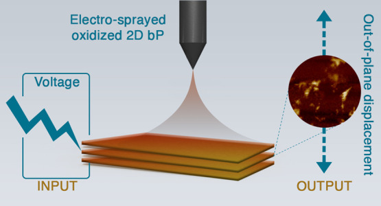
Bidimensional (2D) materials are nowadays being developed as outstanding candidates for electronic and optoelectronic components and devices. Targeted applications include sensing, energy conversion, and storage. Phosphorene is one of the most promising systems in this context, but its high reactivity under atmospheric conditions and its small-area/lab-scale deposition techniques have hampered the introduction of this material in real-world applications so far. However, phosphorene oxides in the form of low-dimensional structures (2D POx) should behave as an electroresponsive material according to recent theoretical studies. In the present work, we introduce electrospraying for the deposition of stoichiometric and large-area 2D POx nanoflakes starting from a suspension of liquid-phase-exfoliated phosphorene. We obtained 2D POx nanostructures with a mean surface area two orders of magnitude larger than phosphorene structures obtained with standard mechanical and liquid exfoliation techniques. X-ray spectroscopy and high-resolution electron microscopy confirmed the P2O5-like crystallographic structure of the electrosprayed flakes. Finally, we experimentally demonstrated for the first time the electromechanical responsivity of the 2D P2O5 nanoflakes, through piezoresponse force microscopy (PFM). This work sheds light on the possible implementation of phosphorus oxide-based 2D nanomaterials in the value chain of fabrication and engineering of devices, which might be easily scaled up for energy-harvesting/conversion applications.
Keywords: phosphorene, bidimensional material, large-area, electrospray, electroresponsive, actuators
Introduction
In the last decade, the scientific community has focused its attention to bidimensional (2D) nanomaterials, considering this class of systems as highly effective and versatile building blocks for the development of new-generation electronic/optoelectronic devices.1,2 Graphene is surely the most studied within 2D materials, but there has been an increasing interest also in the research on new 2D systems, especially semiconducting ones such as transition-metal dichalcogenides (TMDCs) and 2D xenes, i.e., silicene, phosphorene, and borophene.3 Phosphorene (or 2D bP) is an atomically thin 2D material that can be obtained from the exfoliation of layered bulk black phosphorus (bP). It shows a lot of interesting properties, such as a direct band gap dependent on the number of atomic layers (0.3–2 eV),4 high charge mobility (103 cm2/V s),5 and high photoluminescence quantum yield.6
The high reactivity of phosphorene when exposed to air7 is surely one of the most difficult challenges to face to easily use this nanomaterial for large-scale applications.8 To protect the material from oxygen, different approaches have been developed, including the direct blending of the phosphorene flakes into a polymeric matrix,9,10 or the deposition of a protective/passivating layer,11,12 as shown in our previous works.13,14 However, the burial of phosphorene into matrices or under protective layers lengthens and complicates process protocol regardless of the desired technological application, from electronic and optoelectronic devices to energy storage and conversion, to chemical sensing.
Otherwise, one could take advantage of the nontrivial properties of low-dimensional phosphorene oxides, or 2D POx. 2D POx have recently attracted the community for their potential application in electronic, optoelectronic, and energy-harvesting fields, in general.
Ab initio calculations have revealed that the electronic structure of 2D POx is strongly dependent on the oxygen concentration, showing a band gap ranging from 4 to 10 eV and an exciton binding energy (Eb) ranging from 1.4 to 3.0 eV, when passing from a low to a high oxygen content (from P4O2 to P4O10).15 Consequently, both optical and optoelectronic properties in these materials strongly depend on the content/coverage of oxygen. Besides the electronic structure, another recent theoretical study reports that the loss of the mirror symmetry in 2D POx nanostructures, compared to pristine phosphorene, leads to a reduction of the phonon lifetime and consequently to great reduction of thermal conductivity. These characteristics make 2D POx nanostructures promising candidates for low-dimensional thermoelectric devices.16 In addition, thanks again to its noncentrosymmetric structure, recent theoretical calculations17,18 predicted that 2D POx should show piezoelectric properties. Piezoelectricity, which is the ability to reversibly convert mechanical energy into electrical energy, is a property shared between many materials with a noncentrosymmetric crystalline structure, such as many metal oxides19 and metal dichalcogenides.20,21 Also, 2D materials such as transition-metal dichalcogenides (TMDCs) or 2D xenes exhibit enhanced piezoelectric properties19 with respect to bulk piezoelectric materials. Thus, piezoelectric 2D materials are ideal candidates for applications such as nanosensors,22,23 actuators,24,25 and energy harvesters,26−29 which can operate without an external power supply for sensing, data processing, and data transmission, as highly desired for the Internet-of-Things (IoT).
Here, we introduce an electrospraying technique as an innovative and effective method for the deposition of large-area 2D POx nanostructures, which exhibit electromechanical response. The electrospray process, which is based on the application of an electric voltage bias (i.e., tens of kilovolt) between a liquid solution and a collector, has been recently introduced as a scalable method for the deposition of large-area electrodes for applications in solar cells30 and supercapacitors.31 Once the applied electric field overcomes the surface tension of an element of fluid formed at the termination of an electrified extruder, in fact, charged droplets are formed and sprayed, namely, accelerating toward the collector. Here, the electrospray process was applied to a dispersion of phosphorene (2D bP) flakes in dimethylsulfoxide (DMSO), leading to the formation of crystalline 2D POx structures, with an aspect ratio as high as 10 000 (thickness vs lateral dimensions). X-ray photoelectron spectroscopy (XPS), energy-dispersive X-ray analysis (EDX), and transmission electron microscopy (TEM) are used to analyze the composition and the crystalline structure of the deposited 2D nanomaterial. Morphological and mechanical studies are carried out by optical microscopy and atomic force microscopy (AFM). In addition, for the first time, the electroresponsive properties of the deposited 2D nanomaterial are experimentally demonstrated through piezoresponse force microscopy (PFM), showing that the material responds to external electric fields by displaying both vertical and torsional displacements.
The electroresponsive features of the studied 2D POx nanostructures make them particularly attractive for energy-harvesting/conversion applications.
Experimental Section
bP Synthesis
bP was synthesized according to the method published by Lange, as previously reported by our group.13,14 Red phosphorus is used as P-source, and Au, Sn, and SnI4 are used as mineralizing agents and catalysts. The mixture is heated in an evacuated quartz vial at temperature T = 650 °C for 3 days32,33 and then cooled very slowly at room temperature.
Liquid-Phase Exfoliation
Liquid-phase exfoliation of bP has been extensively studied during the last years. Solvents such as dimethylsulfoxide (DMSO) and dimethylformamide (DMF), which both show a high dielectric constant and high surface tension, have been largely used.34 Molecular dynamics simulations have shown that the cohesion energy between the solvent molecules and the bP layers is of great importance, explaining why DMSO, which has a strong affinity with phosphorene, ensures great stability of the dispersion.35
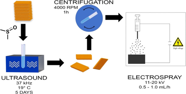
In this work, to a suspension of bP microcrystals (5.0 mg) in 5.0 mL of DMSO, deoxygenated distilled water (3–5 μL) was added and the mixture was sonicated for 5 days in the dark keeping the bath temperature at T = 19 °C. The obtained 2D bP suspension was either used as it is or after centrifugation for 1 h at 4000 rpm and after collection of the supernatant fraction, for the deposition through electrospray.
Mechanical Exfoliation
Mechanically exfoliated 2D bP was produced as a reference sample. A bulk bP crystal was mechanically exfoliated in a controlled atmosphere with the scotch tape method (35 times folding). 2D bP flakes obtained in this way were then transferred onto cleaned silicon substrates.
Deposition of 2D POx by Electrospraying
Electrospraying has been recently applied also for the deposition of a variety of large-area 2D materials, including graphene 2D and three-dimensional (3D) structures31 and GO.
Here, the whole process was conducted in air and in the absence of heating. The 2D bP suspension obtained from the liquid-phase exfoliation whose concentration is 1 mg/mL (see the description above) was pumped through a syringe into a stainless steel nozzle (inner diameter, 200 μm) at a speed 0.5–1.0 mL/h, by applying a voltage of 11–20 kV between the nozzle and a metal support at a distance of 15 cm (where the deposition occurs).
Deposition of the Suspension onto Silicon Substrate Previously Coated with 40 nm of Gold
To estimate the total amount of phosphorene oxide obtained by a single electrospray deposition of the 2D bP suspension, we might take into account (i) a reduction of about 25% of the starting concentration (1 mg/mL) of the suspension after centrifugation at 5000 rpm36 and (ii) that in a single deposition process of 5 min, the solution used is 0.083 mL. In this scenario, an amount of 0.06 mg of phosphorene oxide is obtained by a single deposition process, which corresponds to a deposition rate of 0.73 mg/h.
X-ray Photoelectron Spectroscopy (XPS)
XPS analysis was carried out using an ESCALAB 250 Xi, equipped with a monochromatic X-ray source (Al Kα = 148.6 eV) and 6 Channeltron as the detection system. All samples were fixed to a steel sample holder by a metallic clip. The spectra were recorded at 50 eV pass energy at a pressure in the analysis chamber of about 10–10 mbar. The BE scale was calibrated positioning the adventitious carbon contribution at BE = 285.0 eV. All data were collected and processed using the Avantage v5.9 software. A signal from a localized spot of 50 μm2 of lateral size has been used to analyze a homogeneous area of the selected sample.
AFM
Topographic AFM of 2D bP and POx flakes were performed in PeakForce Tapping mode using Bruker SNL-A probes with a nominal spring constant of 0.35 N/m (Bruker) on a Bruker Multimode 8 microscope equipped with a Nanoscope V controller and a type JV piezoelectric scanner. Force/distance curves were recorded using the same setup at a maximum applied load of 10 nN. The deflection sensitivity of each probe was determined on a silicon oxide surface, and its spring constant was measured with the thermal noise method. All AFM measurements were performed in an atmospheric hood under a gentle flow of either dry nitrogen or air (∼50% humidity) to, respectively, inhibit or promote oxidation. Raw images were processed with Gwyddion37 v2.53. Force/distance curves were analyzed with Hooke38 rev213.
PFM Studies
PFM measurements were performed on PO flakes electrosprayed onto silicon substrates, previously coated with 40 nm of gold. A Bruker Dimension Icon system equipped with a Nanoscope V controller was employed as the SPM system. Measurements were carried out in peak force mode, using a platinum–iridium-coated tip with a nominal radius of 20 nm and an elastic constant of 2.8 N/m.
Transmission Electron Microscopy
Transmission electron microscopy (TEM) was carried out using a Thermo Fischer Tecnai F20 microscope, operated at a 120 kV accelerating voltage to reduce beam damage during observations. Samples from liquid-phase exfoliation were prepared by simple drop-casting of the solutions over a conventional holey-carbon TEM grid and immediately loaded in the microscope to prevent long-term air exposure. Samples of electrosprayed 2D POx were prepared by securing a conventional copper TEM grid, covered with a holey-carbon film, over a highly conductive silicon substrate using a drop of conductive silver paint. The electrospraying deposition procedure as described above was performed and the grid is later released from the substrate and loaded inside the microscope for characterization.
Scanning Electron Microscopy (SEM) and EDX
Scanning electron microscopy (SEM) was performed with an FEI Nova NanoSEM 450 system, equipped with an energy-dispersive X-ray (EDX) detector and operating at acceleration voltages of 5–10 kV (Scheme 1).
Scheme 1. Schematic Illustration of the Deposition of 2D POx Flakes Using the Electrospraying Technique, Starting from Liquid-Phase-Exfoliated bP.
Results and Discussion
Morphological Characterization
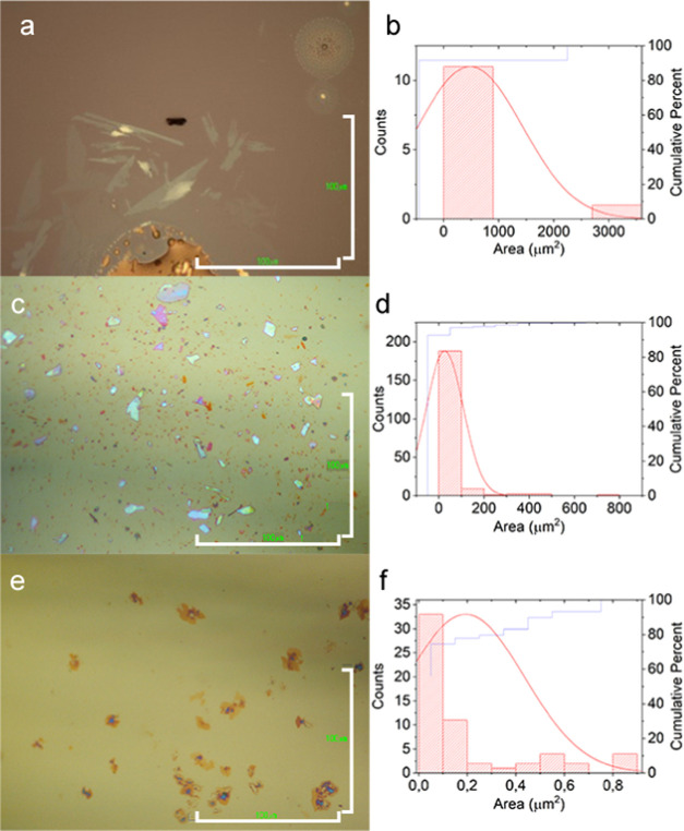
Given the affinity of bP to oxygen, by performing the whole electrospraying process in air, we aimed at depositing a material containing oxidized forms of bP. As the first characterization of the deposited material, we used optical microscopy to analyze the size distribution and the aspect ratio, together with the possible presence of solvent impurities. Optical images of flakes deposited by electrospray were compared with 2D bP samples prepared through liquid-phase exfoliation and oxygen-free mechanical exfoliation of bP. Optical microscopy highlights that the largest elongated solid structures are generally observed closer to big drops of solvent (Figure 1a). In particular, the observed structures have sharp edges and lateral dimensions that range from tens to hundreds of μm2, with a very low and homogeneous optical contrast, thus indicating a crystalline 2D nature of the material deposited. It is worth noticing that, unlike previous reports on MXene electrosprayed flaxes,39 where crumpled 3D morphologies of the flakes are reported, here, the use of a high-boiling-point solvent (DMSO, boiling point: 189 °C) could enable a more gentle deposition of the flakes onto the collector, thus avoiding the fragmentation and wrinkling processes, which might be associated with a fast evaporation of the solvent during the time of flight.
Figure 1.
Typical optical micrographs of samples of: (a) 2D structures deposited by electrospraying and (b) relative surface area distribution; (c) 2D bP flakes obtained from the mechanical exfoliation of bP and (d) relative surface area distribution; (e) 2D bP obtained by drop-casting a suspension of liquid-phase-exfoliated bP and (f) relative surface area distribution. Scale bar: 100 μm.
On the contrary, the optical images of mechanically exfoliated bP (Figure 1c) or liquid-phase-exfoliated bP (Figure 1e) indicate that much smaller crystalline flakes are obtained with these two techniques. Moreover, mechanical and liquid-phase exfoliation produces crystalline flakes with a wide distribution of lateral sizes and thicknesses (evaluated through optical contrast13).40 For a quantitative comparison, the mean surface areas of the 2D flakes deposited by electrospraying, mechanical exfoliation, and liquid-phase exfoliation were calculated, resulting in 480, 26.3, and 0.2 μm2, respectively (Figure 1b,d,f). These values clearly highlight the effectiveness of the proposed method for the deposition of large-area 2D structures.
The morphology of the 2D structures obtained by electrospraying was further analyzed through AFM. In many regions of each substrate, single-layer 2D structures are found (Figure 2a). The surface of these structures is atomically flat (full width at half-maximum (FWHM) of peak height is <1 nm) and extends over a micrometric area. It should be noted that the uniform thickness of these flakes is fundamental in view of their application in electronics because the electronic properties are strongly thickness-dependent. In addition, the morphology of the single-layer structures is highly stable and remains unchanged after overnight exposure to air, as observed from the AFM image taken on the same surface of the same 2D flake (Figure S1 in the Supporting Information). This is in striking contrast to that typically found for mechanically exfoliated 2D bP, since the first oxidation features are already observed within 1 h after air exposure.13
Figure 2.
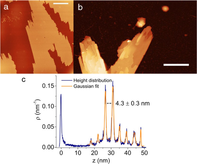
AFM height image of (a) a single-layer flake and (b) a multilayered flake, obtained through electrospray. (c) Height distribution of the multilayered flake as extracted from image (b). Scale bar: (a) 30 μm; (b) 5 μm. Vertical scales: (a) −10–20 nm; (b) −5–55 nm.
By contrast, the thermal stability of electrosprayed POx flakes in inert atmosphere is lower compared to mechanically exfoliated 2D bP. The optical images before and after annealing at 400 °C for 15 min (Figure S2) show the total removal of POx flakes from SiO2 substrate due to the thermal treatment. Instead, annealing at 200 °C, for the same time (15 min) resulted in only a partial removal of POx flakes. We can assume that POx flakes are stable at temperatures lower than 200 °C (Figure S3). It is likely that annealing at temperatures higher than 200 °C leads to the complete removal of the POx flakes due to their weak adhesion onto the SiO2 substrate, which may be further weakened or inhibited by the presence of residual solvent from the electrospray process.
On the contrary, 2D bP flakes obtained by mechanical exfoliation and transferred onto SiO2 substrates are thermally stable up to 600 °C. XPS spectra of 2D bP flakes onto SiO2 (Figure S4, Table S1) show indeed that the energy of the P 2p signal related to phosphorous remains unaltered before and after the annealing process, revealing the high thermal stability of nonoxidized 2D bP. We can conclude that more favorable interactions probably occur between mechanically exfoliated 2D bP flakes and SiO2, compared to electrosprayed POx flakes onto SiO2.
2D multilayered structures can be also found (Figure 2b). The height distribution graph obtained from the AFM images of the 2D multilayered structure reveals that the layers are equally separated by an average distance of about 4.3 ± 0.3 nm (Figure 2c). This indicates that the electrosprayed 2D material obtained is layered, like 2D bP, but it has a different crystalline structure and composition, since its interlayer distance is different from that in pristine 2D bP (5.28 Å)41 and also different from that expected from 2D bP intercalated with solvent molecules (i.e., 5.4 Å).42
Moreover, the repeated AFM scans on the same area of the same flake (Figure 3a) highlighted a larger fragility of the electrosprayed material with respect to the mechanical exfoliated 2D bP. For instance, after 15 min of scanning (Figure 3b), the AFM image reveals a hole in the center of the flake, which widens during further scans (Figure 3c). The majority of force curves recorded on intact regions of single-layer electrosprayed flakes show a sharp breakthrough event of a 4.5 nm thick layer at around 1–3 nN applied force (Figure 3d). In contrast, single- or few-layer pristine 2D bP flakes remain unperturbed over 270 min under the same AFM scanning conditions and do not show layer breakthrough events when subjected to forces up to ∼5 nN (see Figure 3d, blue line). The higher brittleness of the oxidized material seems to further confirm the presence of a material with chemical composition and crystalline habit that are different from 2D bP. In detail, this mechanical behavior is predicted by theoretical calculations recently reported in the literature for phosphorene oxides.43
Figure 3.

Mechanical response of single electrosprayed flake as observed via AFM. (a–c) Mechanical failures induced by repeatedly scanning the same 1 × 1 μm2 area (dashed white lines) at 1 nN applied force in PeakForce mode (512 × 512 lines, 0.5 Hz scan rate). After each successive scan, the flake was then imaged at approximately 250 pN applied force at a lower magnification to appreciate potentially induced damages. Failures are apparent after 51 min of total scanning at higher forces (c). (d) Representative nanoindentation force/separation curves performed on electrosprayed flake (red) or a mechanically exfoliated 2D bP flake (blue). The red trace shows a clear breakthrough event with first contact occurring at 4.7 nm and failure at 3.9 nm. The vast majority (96%) of force curves performed on electrosprayed flakes showed one or more breakthrough events of this type, whereas no sudden mechanical failure “steps” were observed on mechanically exfoliated 2D bP flakes subjected to the same compressive stresses. Scale bar: 250 nm.
Compositional, Chemical, and Structural Characterization
To verify the composition of the deposited material, we performed the chemical characterization of the surface of the samples. Due to the heterogeneity of the electrosprayed samples (also related to the presence of solvent droplets onto the substrate and to the subsequent solvent evaporation pattern), XPS, EDX, and TEM analyses were performed only on selected areas of the substrate, where the 2D structures were observed by optical microscopy.
XPS measurements of electrosprayed samples were compared to those of mechanically exfoliated 2D bP as the reference. In particular, the oxidation state of the phosphorus atoms in the two samples was investigated.
Figure 4 shows the P 2p spectra of both samples. P 2p peak is characterized by the typical doublet due to the spin–orbit splitting P 2p3/2–P 2p1/2, separated by Δ(BE) = 1.3 eV. This signal is generally found in the range of binding energy (BE) = 129.0–135.0 eV, depending on the bond in which P is involved. To avoid the plasmon loss of Si 2p that for Si(0) lies in the proximity of the P 2p signal, electrospray and mechanical exfoliations were performed on silicon substrates covered with a thermally grown layer of SiO2. The mechanically exfoliated 2D bP sample was characterized by a P 2p3/2 peak positioned at BE = 130.0 eV, which is characteristic for P–P bond.44 The good quality of 2D bP was also testified by the absence of oxides contribution, generally positioned at higher BE.45 In the case of the electrosprayed sample, the P 2p3/2 peak was positioned at BE = 134.1 eV, which is typical for P at a higher oxidation state (+5), in the configuration of P2O5. The absence of a peak positioned at BE = 130.0 eV highlights that none (or a negligible part) of the P atoms in electrosprayed sample are in the 0 oxidation state, such as in BP. These results highlight and confirm that the proposed electrospray deposition is a good method to produce an oxidized phosphorus-based material (2D POx).
Figure 4.
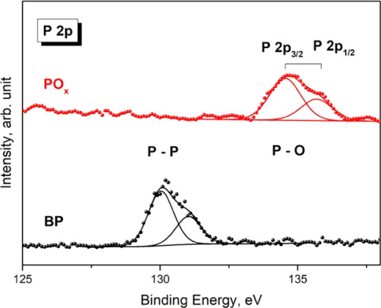
XPS spectra of P 2p acquired on mechanically exfoliated 2D bP and electrosprayed samples.
Other than P signals, the XPS quantitative analysis revealed also the presence of other elements, such as C, O, N, and Si (Table S2). The Si 2p signal was assigned to the substrate because the information depth of the XPS is higher than the thickness of 2D POx. The C 1s signal was characterized by two components positioned at BE = 285.0 eV (14.8 atom %) and 286.6 eV (1.6 atom %), assigned to aliphatic carbon and C–O bond, respectively. As regards the O 1s signal, there was a strong contribution of SiO2 at 533.1 eV (52.1 atom %), while the contribution of P–O and C–O was found at BE = 531.2 eV (3.6 atom %). Finally, the presence of N was detected, where N 1s signal was positioned at BE = 402.4 eV, assigned to residual NO groups from the sample preparation.
The local analysis through SEM microscopy and EDX spectroscopy confirmed that the signal from oxidized species identified by XPS can be attributed to the electrosprayed material.
Figure 5a shows the SEM image of the sample prepared through electrospraying, and Figure 5b shows the corresponding elemental analysis map extrapolated from EDX measures on the same area. The darker areas of the SEM image correspond to phosphorus-rich areas, while on the substrate, only Si and O signals are registered. The EDX spectrum (Figure 5c) registered at the point X of Figure 5a is characterized by P, Si, and S peaks arising, respectively, from (i) the 2D POx structure observed, (ii) the substrate, and (iii) the residual DMSO solvent in proximity of the 2D structure.
Figure 5.
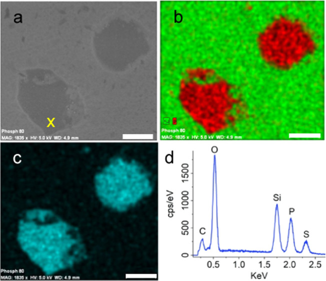
(a) SEM image of 2D POx flakes. (b, c) Phosphorus (red), silicon (green), and oxygen (cyan) EDX maps recorded from the 2D POx flakes shown in (a). (d) EDX spectrum taken at the point indicated with X in (a). Scale bar: 30 μm.
While the composition of the electrosprayed structures was confirmed through XPS and EDX analyses, TEM was performed to investigate their crystalline features.
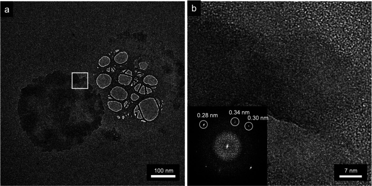
Figure 6a shows a POx aggregate over the amorphous carbon film of the TEM grid, with a rather regular circular shape, probably originating from a nanodroplet of the spray procedure. It should be revealed that the size and shape of the POx flakes deposited through electrospraying are largely dependent on the substrate, explaining why POx flakes analyzed by TEM have smaller lateral dimensions and different shapes with respect to the flakes deposited over Si or Si/SO2 substrates and analyzed through XPS, AFM, and PFM. The area highlighted in the white rectangle is further magnified in the high-resolution electron microscopy (HREM) image in Figure 6b, where lattice fringes are visible. The fast Fourier transform (FFT) of the image is shown in the inset: the marked spots correspond to periodicities of 0.34, 0.30, and 0.28 nm. While the exact crystal orientation was impossible to be determined, the periodicities shown here are compatible with the crystal structure of P2O5 found in the literature,46 namely, (120) 0.335 nm, (211) 0.305 nm, and (220) 0.283 nm, consistent with the composition found by XPS analysis.
Figure 6.
TEM characterization of electrosprayed 2D POx material. (a) TEM image of crystal aggregate over the amorphous carbon film of the TEM grid. (b) HREM image of the area highlighted by the white rectangle in (a), showing lattice fringes of the deposited material; (inset) FFT of the HREM image showing reflections corresponding to planes spaced by 0.34, 0.30, and 0.28 nm, compatible with the P2O5 crystal structure.
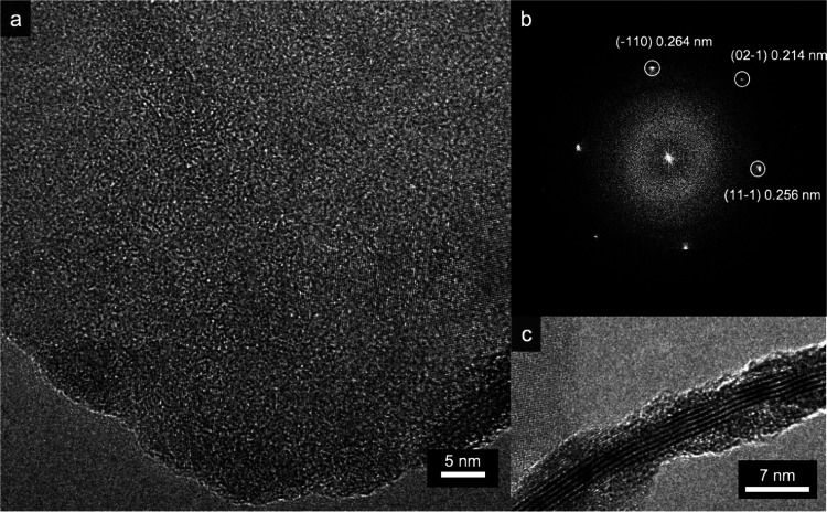
TEM analysis of 2D bP obtained by liquid-phase exfoliation of bulk bP exhibits largely different results from the electrosprayed samples. Figure 7a shows the HREM image of the edge of a bP nanosheet, and Figure 7b displays the corresponding FFT, where reflections compatible with bP crystal structure are highlighted. The flake is oriented with the (112) direction aligned with the viewing direction, showing (1̅10), (021̅), and (111̅) reflections in the FFT. When the flake edge folds over itself, (002) lattice fringes, spaced by 0.525 nm, are visible in the HREM image, as shown in Figure 7c, and the number of stacked layers can be determined by counting the number of fringes visible in the image (six layers, in the case of the shown image).
Figure 7.
TEM characterization of liquid-phase-exfoliated bP. (a) High-resolution TEM (HRTEM) image of a black phosphorous flake edge. (b) FFT of the image, showing black phosphorous (1̅10), (021̅), and (111̅) reflections. (c) Details of the flake folded edge, showing (002) lattice fringes.
Electromechanical Responsivity
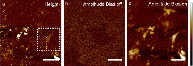
Piezoresponse force microscopy (PFM) probes the surface mechanical deformations of a material in response to an external voltage applied between an AFM tip and a bottom electrode (usually a conductive substrate underneath the investigated sample). This might unveil the electromechanical functionality of the material at the nanometer and micrometer scales. The applied voltage is Vext = Vdc + Vac × cos(ωt), where Vdc is an optional dc offset and Vac is the amplitude of the alternated voltage with angular frequency ω. In electromechanically active materials, the surface can deform mechanically in response to the external electric field. By the use of a position-sensitive detector for the cantilevered probe, the PFM technique can track both out-of-plane and in-plane components of the material response at the modulated frequency by lock-in detection, which is generally useful for systems with an arbitrary polarization direction. Electromechanically active materials exhibit a nonzero amplitude PFM signal when an external field is applied. Figure 8a shows a typical AFM image of electrosprayed 2D P2O5 flakes. The corresponding out-of-plane amplitude images, when no bias is applied to the tip-sample system and upon the application of 5 V, are reported in Figure 8b,c.
Figure 8.
AFM topographic image and the corresponding PFM image at bias voltages 0 V (b) and 5 V (c). Scale bar: 3 μm. Vertical scales: (a) −12–20 nm; (b, c) −17–30 pm.
Micrographs clearly indicate that 2D P2O5 flakes are sensitive to the applied external field and generate a strain response of the order of tens of picometers. A more in-depth investigation of the electromechanical response of one of the flakes in Figure 8a is reported in the Supporting Information (Figure S5b,c with out-of-plane and in-plane amplitude signals recorded at Vdc = 0, Vac = 5 V, and a frequency of 30 kHz). Out-of-plane and in-plane signals, both as amplitude and phase signals, have a similar spatial distribution that well matches the topography, thus indicating the presence of both vertical and torsional displacements (related to domains sensitive to shear forces), which can be correlated to domain patterns oriented at certain angles with respect to the sample plane. The phase image in Figure S5d indicates an out-of-phase response (i.e., flakes appear dark), corresponding to dipoles oriented toward the bottom electrode. Out-of-plane dipoles are sensitive to the direction of the applied field and exhibit a 180° phase shift (i.e., flakes appear bright) when the external bias is inverted (i.e., the positive bias is applied to the sample and the tip is grounded) as reported in Figure S5e. Note that the amplitude of the out-of-plane signal, some picometers per V (4–5 pm/V), is comparable to the theoretical values reported in the literature for phosphorene oxides.17 Moreover, the out-of-plane amplitude intensity increases with the thickness of P2O5 flakes (Figure 9).
Figure 9.
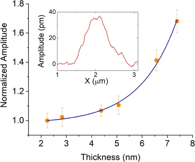
Maximum out-of-plane amplitude intensity vs flake thickness (black dots). The line is a guide to the eye. Inset: Typical out-of-plane amplitude profile.
This behavior is in agreement with previous reports on flakes of 2D materials such as sulfides and selenides47,48 and can be ascribed to a nonuniform distribution of the electric field in the tip-sample system, especially for materials with low electrical permittivity.49,50 The presence and amplitude of the out-of-plane piezoresponse signals and their increment versus thickness, allow us to include electrosprayed 2D P2O5 in the class of electromechanical responsive materials. Envisaged applications, for which electrosprayed 2D P2O5 might establish new design rules, include hybrid nanoelectronics/nanogenerator platforms, optomechanical devices, and sensing architectures based on shear or strained components.
Conclusions
In summary, we demonstrated that the electrospraying technique is a useful tool to effectively deposit an air-stable, phosphorus oxide-based nanomaterial in the 2D form, specifically as 2D P2O5 nanoflakes as confirmed by the XPS, SEM-EDX, and HRTEM analyses. AFM confirmed that the electrosprayed, large-area P2O5 nanostructures have an atomically flat surface, a thickness in the nanometer range (single-layered structures), and a periodicity between layers of about 4.3 ± 0.3 nm (few-layer structures), confirming the extremely high surface-to-volume ratio and 2D nature of such P2O5 structures. AFM also confirmed the higher stability in air and higher mechanical fragility of the 2D P2O5 nanoflakes with respect to 2D bP. Notably, the lateral size of the electrosprayed 2D P2O5 flakes (hundreds of μm2) is much larger than the average lateral size of 2D bP flakes obtained with standard techniques such as mechanical and liquid-phase exfoliation of bP (tens of μm2). Other than the larger lateral size and the improved stability, the electrosprayed 2D P2O5 flakes showed a clear electromechanical responsivity. PFM was indeed performed onto the electrosprayed 2D P2O5 flakes to demonstrate their electromechanical response, confirming theoretical predictions from the literature on 2D oxidized phosphorus nanostructures. The electrosprayed 2D P2O5 flakes show in fact both in-plane signal (tenths of picometers per volt) and out-of-plane signal (some picometers per volt) when subjected to an external electric field.
Overall, the approach herein proposed to deposit a large-area, electromechanical responsive 2D P2O5 allows us to overcome the process scalability issues and enables the real applicability of phosphorus-based 2D nanomaterials for sensing and various classes of energy-harvesting devices.
Acknowledgments
The European Research Council (ERC) and the National Research Council of Italy (CNR) are acknowledged for funding the work through the project PHOSFUN, an ERC Advanced Grant assigned to M.P. as PI (grant agreement no. 670173). The authors acknowledge financial support from the Institute for the Study of Nanostructured Materials (ISMN) of the National Research Council of Italy (CNR) through the project MAT4BIO “Materiali innovativi per la produzione di Biodiesel in one-step” from Institute Projects 2018. They also acknowledge the PRIN 20173L7W8K project funded by Italian Minister of Research.
Supporting Information Available
The Supporting Information is available free of charge at https://pubs.acs.org/doi/10.1021/acsanm.0c03465.
Optical, AFM, PFM, and XPS characterizations of oxidized phosphorene obtained by electrospray deposition (PDF)
Author Contributions
The manuscript was written through contributions of all authors. All authors have given approval to the final version of the manuscript.
The authors declare no competing financial interest.
Supplementary Material
References
- Yang A.; Wang D.; Wang X.; Zhang D.; Koratkar N.; Rong M. Recent Advances in Phosphorene as a Sensing Material. Nano Today 2018, 20, 13–32. 10.1016/j.nantod.2018.04.001. [DOI] [Google Scholar]
- Li P.; Zhang D.; Jiang C.; Zong X.; Cao Y. Ultra-Sensitive Suspended Atomically Thin-Layered Black Phosphorus Mercury Sensors. Biosens. Bioelectron. 2017, 98, 68–75. 10.1016/j.bios.2017.06.027. [DOI] [PubMed] [Google Scholar]
- Franklin A. D. Nanomaterials in Transistors: From High-Performance to Thin-Film Applications. Science 2015, 349, aab2750 10.1126/science.aab2750. [DOI] [PubMed] [Google Scholar]
- Liu H.; Neal A. T.; Zhu Z.; Luo Z.; Xu X.; Tománek D.; Ye P. D. Phosphorene: An Unexplored 2D Semiconductor with a High Hole Mobility. ACS Nano 2014, 8, 4033–4041. 10.1021/nn501226z. [DOI] [PubMed] [Google Scholar]
- Morita A. Semiconducting Black Phosphorus. Appl. Phys. A: Mater. Sci. Process. 1986, 39, 227–242. 10.1007/BF00617267. [DOI] [Google Scholar]
- Wang X.; Jones A. M.; Seyler K. L.; Tran V.; Jia Y.; Zhao H.; Wang H.; Yang L.; Xu X.; Xia F. Highly Anisotropic and Robust Excitons in Monolayer Black Phosphorus. Nat. Nanotechnol. 2015, 10, 517–521. 10.1038/nnano.2015.71. [DOI] [PubMed] [Google Scholar]
- Luo W.; Zemlyanov D. Y.; Milligan C. A.; Du Y.; Yang L.; Wu Y.; Ye P. D. Surface Chemistry of Black Phosphorus under a Controlled Oxidative Environment. Nanotechnology 2016, 27, 434002 10.1088/0957-4484/27/43/434002. [DOI] [PubMed] [Google Scholar]
- Telesio F.; le Gal G.; Serrano-Ruiz M.; Prescimone F.; Toffanin S.; Peruzzini M.; Heun S. Ohmic Contact Engineering in Few–Layer Black Phosphorus: Approaching the Quantum Limit. Nanotechnology 2020, 31, 334002 10.1088/1361-6528/ab8cf4. [DOI] [PubMed] [Google Scholar]
- Telesio F.; Passaglia E.; Cicogna F.; Costantino F.; Serrano-Ruiz M.; Peruzzini M.; Heun S. Hybrid Nanocomposites of 2D Black Phosphorus Nanosheets Encapsulated in PMMA Polymer Material: New Platforms for Advanced Device Fabrication. Nanotechnology 2018, 29, 295601 10.1088/1361-6528/aabd8d. [DOI] [PubMed] [Google Scholar]
- Passaglia E.; Cicogna F.; Lorenzetti G.; Legnaioli S.; Caporali M.; Serrano-Ruiz M.; Ienco A.; Peruzzini M. Novel Polystyrene-Based Nanocomposites by Phosphorene Dispersion. RSC Adv. 2016, 6, 53777–53783. 10.1039/C6RA10133J. [DOI] [Google Scholar]
- Li P.; Zhang D.; Liu J.; Chang H.; Sun Y.; Yin N. Air-Stable Black Phosphorus Devices for Ion Sensing. ACS Appl. Mater. Interfaces 2015, 7, 24396–24402. 10.1021/acsami.5b07712. [DOI] [PubMed] [Google Scholar]
- Li P.; Zhang D.; Wu J.; Cao Y.; Wu Z. Flexible Integrated Black Phosphorus Sensor Arrays for High Performance Ion Sensing. Sens. Actuators, B 2018, 273, 358–364. 10.1016/j.snb.2018.06.077. [DOI] [Google Scholar]
- Bolognesi M.; Brucale M.; Lorenzoni A.; Prescimone F.; Moschetto S.; Korolkov V. V.; Baldoni M.; Serrano-Ruiz M.; Caporali M.; Mercuri F.; Besley E.; Muccini M.; Peruzzini M.; Beton P. H.; Toffanin S. Epitaxial Multilayers of Alkanes on Two-Dimensional Black Phosphorus as Passivating and Electrically Insulating Nanostructures. Nanoscale 2019, 11, 17252–17261. 10.1039/C9NR01155B. [DOI] [PubMed] [Google Scholar]
- Bolognesi M.; Moschetto S.; Trapani M.; Prescimone F.; Ferroni C.; Manca G.; Ienco A.; Borsacchi S.; Caporali M.; Muccini M.; Peruzzini M.; Serrano-Ruiz M.; Calucci L.; Castriciano M. A.; Toffanin S. Noncovalent Functionalization of 2D Black Phosphorus with Fluorescent Boronic Derivatives of Pyrene for Probing and Modulating the Interaction with Molecular Oxygen. ACS Appl. Mater. Interfaces 2019, 11, 22637–22647. 10.1021/acsami.9b04344. [DOI] [PMC free article] [PubMed] [Google Scholar]
- Lu Y.; Zhu X. Superbound Excitons in 2D Phosphorene Oxides. J. Phys. Chem. A 2019, 123, 21–25. 10.1021/acs.jpca.8b09683. [DOI] [PubMed] [Google Scholar]
- Lee S.; Kang S.-H.; Kwon Y.-K. Low Lattice Thermal Conductivity of a Two-Dimensional Phosphorene Oxide. Sci. Rep. 2019, 9, 5149 10.1038/s41598-019-41696-y. [DOI] [PMC free article] [PubMed] [Google Scholar]
- Yin H.; Zheng G.-P.; Gao J.; Wang Y.; Ma Y. Enhanced Piezoelectricity of Monolayer Phosphorene Oxides: A Theoretical Study. Phys. Chem. Chem. Phys. 2017, 19, 27508–27515. 10.1039/C7CP05669A. [DOI] [PubMed] [Google Scholar]
- Li J.; Zhao T.; He C.; Zhang K. Surface Oxidation: An Effective Way to Induce Piezoelectricity in 2D Black Phosphorus. J. Phys. Appl. Phys. 2018, 51, 12LT01 10.1088/1361-6463/aaad98. [DOI] [Google Scholar]
- Xiang H. J.; Yang J.; Hou J. G.; Zhu Q. Piezoelectricity in ZnO Nanowires: A First-Principles Study. Appl. Phys. Lett. 2006, 89, 223111 10.1063/1.2397013. [DOI] [Google Scholar]
- Blonsky M. N.; Zhuang H. L.; Singh A. K.; Hennig R. G. Ab Initio Prediction of Piezoelectricity in Two-Dimensional Materials. ACS Nano 2015, 9, 9885–9891. 10.1021/acsnano.5b03394. [DOI] [PubMed] [Google Scholar]
- Alyörük M. M. Piezoelectric Properties of Monolayer II–VI Group Oxides by First-Principles Calculations. Phys. Status Solidi B 2016, 253, 2534–2539. 10.1002/pssb.201600387. [DOI] [Google Scholar]
- Stampfer C.; Helbling T.; Obergfell D.; Schöberle B.; Tripp M. K.; Jungen A.; Roth S.; Bright V. M.; Hierold C. Fabrication of Single-Walled Carbon-Nanotube-Based Pressure Sensors. Nano Lett. 2006, 6, 233–237. 10.1021/nl052171d. [DOI] [PubMed] [Google Scholar]
- Kingon A. I.; Srinivasan S. Lead Zirconate Titanate Thin Films Directly on Copper Electrodes for Ferroelectric, Dielectric and Piezoelectric Applications. Nat. Mater. 2005, 4, 233–237. 10.1038/nmat1334. [DOI] [Google Scholar]
- Fennimore A. M.; Yuzvinsky T. D.; Han W.-Q.; Fuhrer M. S.; Cumings J.; Zettl A. Rotational Actuators Based on Carbon Nanotubes. Nature 2003, 424, 408–410. 10.1038/nature01823. [DOI] [PubMed] [Google Scholar]
- Park S.; An J.; Suk J. W.; Ruoff R. S. Graphene-Based Actuators. Small 2010, 6, 210–212. 10.1002/smll.200901877. [DOI] [PubMed] [Google Scholar]
- Wang Z. L.; Song J. Piezoelectric Nanogenerators Based on Zinc Oxide Nanowire Arrays. Science 2006, 312, 242–246. 10.1126/science.1124005. [DOI] [PubMed] [Google Scholar]
- Yang R.; Qin Y.; Dai L.; Wang Z. L. Power Generation with Laterally Packaged Piezoelectric Fine Wires. Nat. Nanotechnol. 2009, 4, 34–39. 10.1038/nnano.2008.314. [DOI] [PubMed] [Google Scholar]
- Lee E.; Park J.; Yim M.; Kim Y.; Yoon G. Characteristics of Piezoelectric ZnO/AlN–stacked Flexible Nanogenerators for Energy Harvesting Applications. Appl. Phys. Lett. 2015, 106, 023901 10.1063/1.4904270. [DOI] [Google Scholar]
- Wu W.; Wang L.; Li Y.; Zhang F.; Lin L.; Niu S.; Chenet D.; Zhang X.; Hao Y.; Heinz T. F.; Hone J.; Wang Z. L. Piezoelectricity of Single-Atomic-Layer MoS2 for Energy Conversion and Piezotronics. Nature 2014, 514, 470–474. 10.1038/nature13792. [DOI] [PubMed] [Google Scholar]
- Mahmood K.; Khalid A.; Ahmad S. W.; Qutab H. G.; Hameed M.; Sharif R. Electrospray Deposited MoS2 Nanosheets as an Electron Transporting Material for High Efficiency and Stable Perovskite Solar Cells. Sol. Energy 2020, 203, 32–36. 10.1016/j.solener.2020.04.021. [DOI] [Google Scholar]
- Tang H.; Yang C.; Lin Z.; Yang Q.; Kang F.; Wong C. P. Electrospray-Deposition of Graphene Electrodes: A Simple Technique to Build High-Performance Supercapacitors. Nanoscale 2015, 7, 9133–9139. 10.1039/C5NR00465A. [DOI] [PubMed] [Google Scholar]
- Lange S.; Schmidt P.; Nilges T. Au3SnP7@Black Phosphorus: An Easy Access to Black Phosphorus. Inorg. Chem. 2007, 46, 4028–4035. 10.1021/ic062192q. [DOI] [PubMed] [Google Scholar]
- Caporali M.; Serrano-Ruiz M.; Telesio F.; Heun S.; Nicotra G.; Spinella C.; Peruzzini M. Decoration of Exfoliated Black Phosphorus with Nickel Nanoparticles and Its Application in Catalysis. Chem. Commun. 2017, 53, 10946–10949. 10.1039/C7CC05906J. [DOI] [PubMed] [Google Scholar]
- Kang J.; Wood J. D.; Wells S. A.; Lee J.-H.; Liu X.; Chen K.-S.; Hersam M. C. Solvent Exfoliation of Electronic-Grade, Two-Dimensional Black Phosphorus. ACS Nano 2015, 9, 3596–3604. 10.1021/acsnano.5b01143. [DOI] [PubMed] [Google Scholar]
- Sresht V.; Pádua A. A. H.; Blankschtein D. Liquid-Phase Exfoliation of Phosphorene: Design Rules from Molecular Dynamics Simulations. ACS Nano 2015, 9, 8255–8268. 10.1021/acsnano.5b02683. [DOI] [PubMed] [Google Scholar]
- Kang J.; Wells S. A.; Wood J. D.; Lee J.-H.; Liu X.; Ryder C. R.; Zhu J.; Guest J. R.; Husko C. A.; Hersam M. C. Stable Aqueous Dispersions of Optically and Electronically Active Phosphorene. Proc. Natl. Acad. Sci. U.S.A. 2016, 113, 11688–11693. 10.1073/pnas.1602215113. [DOI] [PMC free article] [PubMed] [Google Scholar]
- Nečas D.; Klapetek P. Gwyddion: An Open-Source Software for SPM Data Analysis. Cent. Eur. J. Phys. 2012, 10, 181–188. 10.2478/s11534-011-0096-2. [DOI] [Google Scholar]
- Sandal M.; Benedetti F.; Brucale M.; Gomez-Casado A.; Samorì B. Hooke: An Open Software Platform for Force Spectroscopy. Bioinformatics 2009, 25, 1428–1430. 10.1093/bioinformatics/btp180. [DOI] [PubMed] [Google Scholar]
- Cho S.; Kim D. Y.; Seo Y. Binder-Free High-Performance MXene Supercapacitors Fabricated by a Simple Electrospray Deposition Technique. Adv. Mater. Interfaces 2020, 7, 2000750 10.1002/admi.202000750. [DOI] [Google Scholar]
- Caporali M.; Serrano-Ruiz M.; Telesio F.; Heun S.; Verdini A.; Cossaro A.; Dalmiglio M.; Goldoni A.; Peruzzini M. Enhanced Ambient Stability of Exfoliated Black Phosphorus by Passivation with Nickel Nanoparticles. Nanotechnology 2020, 31, 275708 10.1088/1361-6528/ab851e. [DOI] [PubMed] [Google Scholar]
- Chen L.; Zhou G.; Liu Z.; Ma X.; Chen J.; Zhang Z.; Ma X.; Li F.; Cheng H.-M.; Ren W. Scalable Clean Exfoliation of High-Quality Few-Layer Black Phosphorus for a Flexible Lithium Ion Battery. Adv. Mater. 2016, 28, 510–517. 10.1002/adma.201503678. [DOI] [PubMed] [Google Scholar]
- Yan Z.; He X.; She L.; Sun J.; Jiang R.; Xu H.; Shi F.; Lei Z.; Liu Z.-H. Solvothermal-Assisted Liquid-Phase Exfoliation of Large Size and High Quality Black Phosphorus. J. Materiomics 2018, 4, 129–134. 10.1016/j.jmat.2018.01.003. [DOI] [Google Scholar]
- Wang G.; Pandey R.; Karna P. Phosphorene Oxide: Stability and Electronic Properties of a Novel Two-Dimensional Material. Nanoscale 2015, 7, 524–531. 10.1039/C4NR05384B. [DOI] [PubMed] [Google Scholar]
- Walia S.; Balendhran S.; Ahmed T.; Singh M.; El-Badawi C.; Brennan M. D.; Weerathunge P.; Karim M. N.; Rahman F.; Rassell A.; Duckworth J.; Ramanathan R.; Collis G. E.; Lobo C. J.; Toth M.; Kotsakidis J. C.; Weber B.; Fuhrer M.; Dominguez-Vera J. M.; Spencer M. J. S.; Aharonovich I.; Sriram S.; Bhaskaran M.; Bansal V. Ambient Protection of Few-Layer Black Phosphorus via Sequestration of Reactive Oxygen Species. Adv. Mater. 2017, 29, 1700152 10.1002/adma.201700152. [DOI] [PubMed] [Google Scholar]
- Yang T.; Dong B.; Wang J.; Zhang Z.; Guan J.; Kuntz K.; Warren S. C.; Tománek D. Interpreting Core-Level Spectra of Oxidizing Phosphorene: Theory and Experiment. Phys. Rev. B 2015, 92, 125412 10.1103/PhysRevB.92.125412. [DOI] [Google Scholar]
- Cruickshank D. W. J. Refinements of Structures Containing Bonds between Si, P, S or Cl and O or N. VI. P2O5, Form III. Acta Crystallogr. 1964, 17, 679–680. 10.1107/S0365110X64001682. [DOI] [Google Scholar]
- Liu F.; You L.; Seyler K. L.; Li X.; Yu P.; Lin J.; Wang X.; Zhou J.; Wang H.; He H.; Pantelides S. T.; Zhou W.; Sharma P.; Xu X.; Ajayan P. M.; Wang J.; Liu Z. Room-Temperature Ferroelectricity in CuInP 2 S 6 Ultrathin Flakes. Nat. Commun. 2016, 7, 12357 10.1038/ncomms12357. [DOI] [PMC free article] [PubMed] [Google Scholar]
- Xue F.; Zhang J.; Hu W.; Hsu W.-T.; Han A.; Leung S.-F.; Huang J.-K.; Wan Y.; Liu S.; Zhang J.; He J.-H.; Chang W.-H.; Wang Z. L.; Zhang X.; Li L.-J. Multidirection Piezoelectricity in Mono- and Multilayered Hexagonal α-In2Se3. ACS Nano 2018, 12, 4976–4983. 10.1021/acsnano.8b02152. [DOI] [PubMed] [Google Scholar]
- Morozovska A. N.; Eliseev E. A.; Kalinin S. V. The Piezoresponse Force Microscopy of Surface Layers and Thin Films: Effective Response and Resolution Function. J. Appl. Phys. 2007, 102, 074105 10.1063/1.2785824. [DOI] [Google Scholar]
- Morozovska A. N.; Svechnikov S. V.; Eliseev E. A.; Kalinin S. V. Extrinsic Size Effect in Piezoresponse Force Microscopy of Thin Films. Phys. Rev. B 2007, 76, 054123 10.1103/PhysRevB.76.054123. [DOI] [Google Scholar]
Associated Data
This section collects any data citations, data availability statements, or supplementary materials included in this article.


