Abstract
Metal halide perovskites have emerged as a promising group of materials for optoelectronic applications such as photovoltaics, light emission, and photodetectors. So-far, in particular, the stability of light-emitting devices is limited, which is in part attributed to the intrinsic ionic conductivity of these materials. High-performance devices inevitably contain heterojunctions similar to other optoelectronic devices based on oxide perovskites, II–VI, or III–V group semiconductors. To enable efficient heterojunctions, ion exchange at the interface between different layers should be controlled. Herein, we report a method that enables to control and monitor the extent of anion intermixing between solution-processed lead bromide and vacuum-deposited lead chloride perovskite films. Taking advantage of the ability to fine tune the layer thicknesses of the vacuum-deposited films, we systematically study the effect of film thickness on anionic intermixing. Using these multiple layers, we prepare proof of principle light-emitting devices exhibiting green and blue electroluminescence.
Keywords: perovskites, heterojunctions, light-emitting diodes, light-emitting electrochemical cells, vacuum deposition, ion-diffusion
Introduction
In modern optoelectronics, epitaxial heterostructures have been employed to achieve superior device performances.1−3 However, in the case of metal halide perovskites, there are only a few reports of perovskite/perovskite heterojunctions published to date.4−6 This is mainly due to processing limitation, especially when different materials are coated from solutions of similar polarity, and to the tendency of halide perovskites to exchange anions.7,8 Developing perovskite–perovskite heterojunctions could therefore improve performances and diversify advanced applications. Besides three-dimensional (3D) cesium lead trihalide perovskites (CsPbX3), several lower dimensional cesium lead halide analogues, such as 2D CsPb2X5 and 0D Cs4PbX6 (where X = Cl–, Br–, I–), exist.9,10 Thin films of these materials can be deposited by adjusting the deposition rates of the precursors during vacuum co-evaporation.11,12 Cs4PbX6 typically shows a high exciton binding energy and a low electronic conductivity, the properties of which can be useful in light-emitting applications. For instance, Liashenko et al. blended Cs4PbBrxCl6–x/CsPbBr3Cl3–x in polyethylene oxide (PEO), which was deposited between indium tin oxide (ITO) and indium gallium (InGa) eutectic electrodes, to fabricate single layer light-emitting diodes (LEDs).13 The Cs4PbBrxCl6–x/CsPbBr3Cl3–x blend showed high photoluminescence quantum yield (PLQY) and good spectral stability thanks to the suppression of halide migration. The latter effect is a consequence of the reduced ionic mobility in the 0D Cs4PbBrxCl6–x phase, as reported elsewhere.12,13
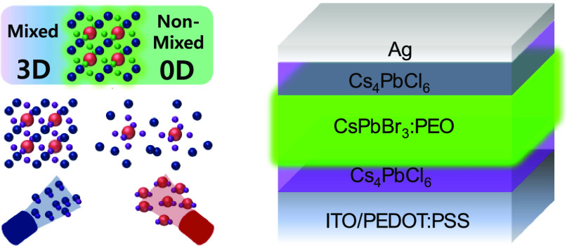
Apart from the control over the material stoichiometry and thickness, vacuum co-evaporation allows the fabrication of multi-layer architecture.14 In this work, we study perovskite heterojunctions combining 3D CsPbBr3 with 0D Cs4PbCl6. CsPbBr3 is employed in a blend with PEO, whose electron lone pairs interact with lead halides resulting in higher PLQYs.15,16 In addition, this polymer–perovskite mixture can form compact films without anti-solvent treatment.17,18 In this work, we deposit perovskite heterojunctions and investigate ion diffusion as well as their optoelectronic properties, in particular by incorporating the heterostructures in LEDs. With this simple structure, it is possible to exclude the effect of transport layers and isolate the physical properties of the perovskite heterojunction.
Results and Discussion
The general deposition method is illustrated in Figure 1a. CsPbBr3 (225 mg, CsBr:PbBr2 molar ratio is 1.5:1) is blended with PEO (150 mg, molecular weight ≈ 600,000 u) and dissolved in 8 mL of dimethyl sulfoxide (DMSO). The solution is then spin-coated on the ITO/PEDOT:PSS layer followed by annealing in vacuum to promote nucleation and formation of compact films.18,19 After this process, the samples are thermally annealed at 70 °C for 3 min to eliminate the residual solvent. The chloride-based films are deposited by vacuum co-sublimation of cesium chloride and lead chloride on top of the solution-processed CsPbBr3:PEO films. The dimensionality of the cesium lead chloride compounds is controlled via the relative deposition rates of the two precursors. Unlike in previous reports, in this study, we do not add any salts to improve the overall device performances.
Figure 1.
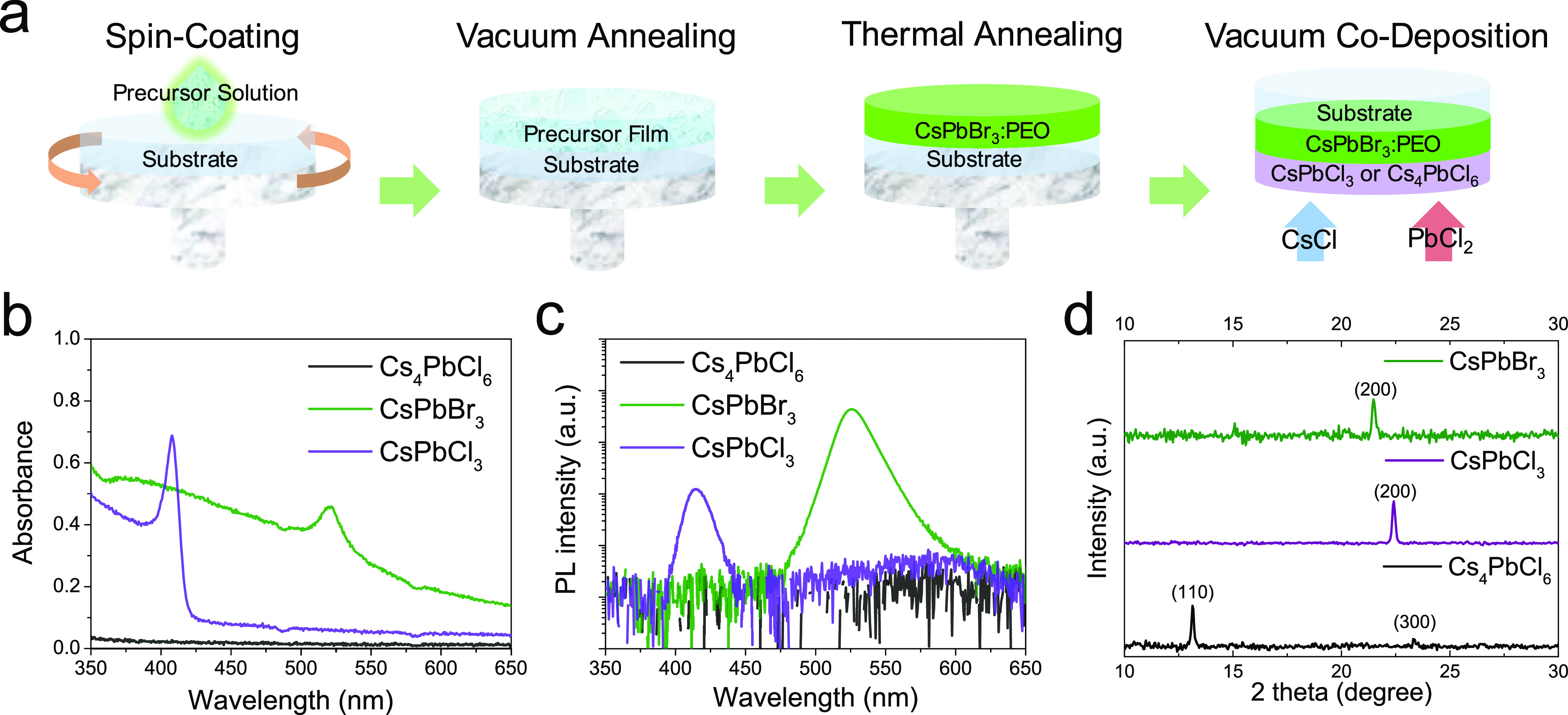
(a) Schematic illustration of the fabrication of lead halide perovskite heterojunctions. (b) Absorbance and (c) photoluminescence spectra (excitation wavelength: 375 nm) and (d) X-ray diffraction patterns of pristine CsPbBr3, CsPbCl3, and Cs4PbCl6 films.
The optical absorption spectra for our solution-processed CsPbBr3 and vacuum-deposited CsPbCl3 and Cs4PbCl6 films are presented in Figure 1b. CsPbBr3 and CsPbCl3 show the characteristic excitonic peaks at 520 and 400 nm, respectively.20 Cs4PbCl6 does not show any absorption in the entire visible region, in view of its band gap of 4.37 eV.21 Upon excitation with a 375 nm laser, CsPbBr3 and CsPbCl3 show photoluminescence (PL) peaks centered at 528 and 405 nm, respectively (Figure 1c), with a small Stokes shift characteristic of direct-band gap bulk 3D perovskites.20 In the case of Cs4PbCl6, we did not observe any PL signal because its band gap is larger than the photon energy at 375 nm. Figure 1d shows the XRD patterns for these three films. The diffractograms of the 3D perovskites show a main peak at 2θ = 21.5° for CsPbBr3 and 2θ = 22.5° for CsPbCl3, which can be ascribed to the (200) plane, which is expected to be the main diffraction signal for non-oriented crystals (see Inorganic Crystal Structure Database, ICSD, references 243734 and 243735). Two characteristic reflections for the 0D Cs4PbCl6 are observed at 2θ = 13.1 and 2θ = 23.3° (see Inorganic Crystal Structure Database, ICSD, references 35703). Note that there is no diffraction peak around a 2θ of 22.5° for the XRD pattern of Cs4PbCl6, which is typical of the (200) plane of the CsPbCl3, which will be helpful in the characterization of the corresponding bilayers (see next section).
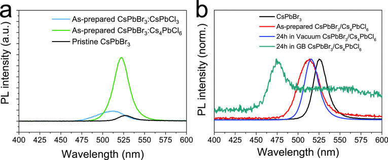
With these three films, heterojunction stacks are fabricated by combining spin-coating and vacuum co-evaporation to investigate the ion-diffusion property at the interface of these materials.4 We initially studied the PL of a 3D/3D heterojunction of the type CsPbBr3 (300 nm)/CsPbCl3 (50 nm) using a 375 nm laser excitation source (Figure 2a). The as-prepared CsPbBr3/CsPbCl3 bilayers show a blue-shifted and asymmetric PL signal with respect to that of the pure CsPbBr3, corresponding to a cyan color emission. This observation is indicative of spontaneous anion exchange between the two materials, even at room temperature. In contrast, the 3D/0D CsPbBr3/Cs4PbCl6 heterojunction shows a negligible PL shift and also a more intense PL as compared to the reference CsPbBr3. This observation is in good agreement with the previous report by Shen et al. who showed hindered anion diffusion and mixing in 0D Cs4PbX6 (X = Cl–, Br–).22
Figure 2.
(a) Photoluminescence spectra of as-prepared CsPbBr3, CsPbBr3/CsPbCl3, and CsPbBr3/Cs4PbCl6 films, and (b) spectra of CsPbBr3 and CsPbBr3/Cs4PbCl6 stored in a vacuum chamber and N2 glovebox (excitation wavelength: 375 nm).
The PL of 3D/0D CsPbBr3/Cs4PbCl6 bilayers was further studied as a function of the storage condition (Figure 2b). We observed a blue shift of the PL signal after storing the bilayer for 24 h in a N2 atmosphere. It is worth to note that this glovebox for storage experiment is a different one from that for the spin-coating, hence the atmosphere is also free of any solvent vapor.
On the contrary, when stored in a vacuum evaporator (base pressure: 2·10–6 mbar) for the same time, the CsPbBr3/Cs4PbCl6 maintained the initial PL peak position. Also, the PL peak was found to be sharper after storing the material in vacuum. This interesting observation agrees with a previous report by Karlsson et al., who showed that in vacuum the material can reorganize and achieve a superior compositional homogeneity, in turn leading to a narrower PL peak.23
In view of the absence of halide mixing in the 3D/0D heterojunctions (CsPbBr3/Cs4PbCl6), as observed by PL, we prepared planar devices combining 0D and 3D metal halide films, in order to study their electroluminescent behavior. In particular, we used CsPbBr3:PEO as the light emitters and studied the effect of the 0D Cs4PbCl6 layer below (at the anode, 0D/3D), on top (at the cathode, 3D/0D), and on both sides of the 3D CsPbBr3 emitter (0D/3D/0D triple layers). The structure of the devices is illustrated in Figure 3a, and they are named following the order and dimensionality of the corresponding heterojunctions. In addition, the flat band diagram is described in the Supporting Information, Figure S1. Since Cs4PbCl6 is a zero-dimensional material with chloride, it forms a type-I structured heterojunction with CsPbBr3 perovskite.
Figure 3.
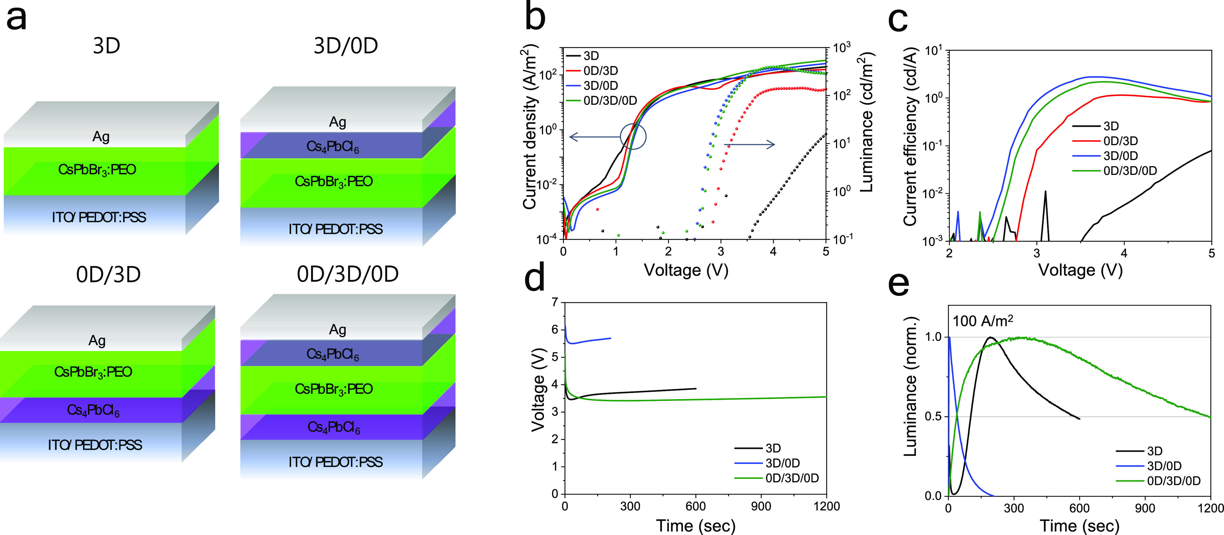
(a) Schematic illustration of the perovskite heterojunction-based light emitters. (b) Current density (lines) and luminance (symbols) vs applied voltage for the same devices. The corresponding current efficiency is shown in (c). (d) Time-dependent voltage and (e) luminance for the same devices driven with a constant current density of 100 A/m2.
The current density and luminance vs voltage (JVL) curves for this device set is reported in Figure 3b. The heterojunction-based devices show a slightly reduced leakage current below 1 V, as compared to the reference single-layer 3D light emitter. More importantly, all heterojunction devices exhibited lower turn-on voltage and more intense electroluminescence as compared to the reference 3D device. In the perovskite heterojunctions, 25 nm thick Cs4PbCl6 films are deposited. After deposition, the main PL peak is slightly blue shifted, suggesting halide intermixing at the 3D/0D interface. Hence, the actual Cs4PbCl6 layer is even thinner compared to the nominal deposited thickness. In this scenario, it is plausible that the lower turn-on voltage originates from interfacial band bending effects favored by the thin Cs4PbCl6 films.
The 3D/0D and 0D/3D/0D devices reached luminance level of about 400 cd/m2, at applied bias of approximately 3.5 V. At the same voltage, device 0D/3D showed lower EL intensity, about one third as compared to the others. As the current density (both in magnitude and profile) is very similar for these three types of devices, their current efficiency (Figure 3c) follows the trend in luminance. The reference 3D device shows a low current efficiency with a maximum of 0.1 cd/A at 5 V. With the 0D layer at the anode (device 0D/3D), the efficiency maximum was improved to 1 cd/A at 4 V, which is further improved when the Cs4PbCl6 0D film is placed in between the CsPbBr3 3D emitter and the cathode. Device 3D/0D and device 0D/3D/0D showed superior efficiency (>3 cd/A), indicating that non-radiative recombination at the CsPbBr3/Ag interface is strongly reduced upon insertion of the 0D buffer layer (as the current density is unvaried between the different device configuration).
In addition to the enhanced performance, we observed a significant improvement in the operational stability of the devices 3D/0D and 0D/3D/0D (Figure 3d,e). To test the stability, the devices were driven with a constant current density of 100 A/m2, while monitoring the evolution of the luminance and voltage. Device 3D/0D was found to be unstable (only a few seconds of operation), while the pristine CsPbBr3-based device shows a half lifetime (t1/2, time to reach half of the maximum luminance) of approximately 10 min. Interestingly, the triple-layer heterojunction device 0D/3D/0D demonstrated a further improved operational stability: with t1/2 = 20 min. The time to reach maximum luminance, 100 cd/m2, in this 0D/3D/0D device was only 25 s (Supporting Information, Figure S2). In addition, this device shows negligible voltage variation (<0.1 V), indicating stable electrical properties, which might arise from the limited and balanced ion movement of the Cs4PbCl6 buffer layers. To clarify the first voltage applied, the initial time vs voltage graph in constant current operation is shown in the Supporting Information, Figure S3. The pristine device and device 0D/3D/0D only need to go through ∼4 V while device 3D/0D needs ∼6 V to apply 100 A/m2. The mechanism responsible for the enhanced stability of the 0D/3D/0D heterojunctions is difficult to identify precisely. It is possible that unbalanced charge injection and subsequent charge accumulation in bilayers might favor non-radiative recombination and trigger the degradation of the perovskite films. Correspondingly, the operational lifetime will be decreased significantly.24,25
Most of all, this limitation on the ion movement by Cs4PbCl6 makes stable electroluminescence. Even after 20 min of the device operation with 100 A/m2, device 0D/3D/0D does not show a blue shift, which stems from halide intermixing. On the contrary, there is a small red shift happening at about 0.2 nm/min (Figure S4) and a recovery of the green emission from CsPbBr3 (from 518 nm to 522 nm). The absorbance, PL, and EL spectra are reported in Figure S5. It is possible that EL recovery in this 0D/3D/0D device originates from the Cl anion diffusing out the radiative recombination zone. After 20 min of device operation, the EL peak (522 nm) becomes similar to that of the pristine device, 526 nm. This phenomenon supports our point that the heterojunction based on 0D cesium lead halide has less chance to donate a halide anion, which causes an emission peak shift.
While avoiding ion diffusion and mixing can be exploited to tune the optoelectronic characteristic of devices (as shown above), controlled anion-mixing is of interest to tune the emission color of perovskite films. Hence, we prepared a series of CsPbBr3/Cs4PbCl6 3D/0D bilayers with constant CsPbBr3 thickness (300 nm) and with different Cs4PbCl6 top-layer thicknesses (0, 25, and 50 nm). These bilayers were treated via solvent vapor annealing (SVA, details in the experimental part) using a modified condition from a previous report, as SVA induces a higher PL intensity compared to slow and spontaneous mixing in nitrogen (Supporting Information, Figure S6).26 From the XRD patterns (Figure 4a), the main (200) diffraction peak, characteristic of the orthorhombic CsPbBr3 phase, shifts to higher angles after anion intermixing with the top layers, although the diffraction intensity is strongly reduced. This is due to partial bromide substitution with chloride, resulting in a smaller unit cell for mixed-halide CsPbBr3–xClx). Importantly, the (110) reflection at 2θ = 12.7°, corresponding to the 0D Cs4PbCl6 phase, is observed even after SVA treatment. This implies that the 3D/0D heterojunction is structurally preserved in spite of halide mixing.
Figure 4.
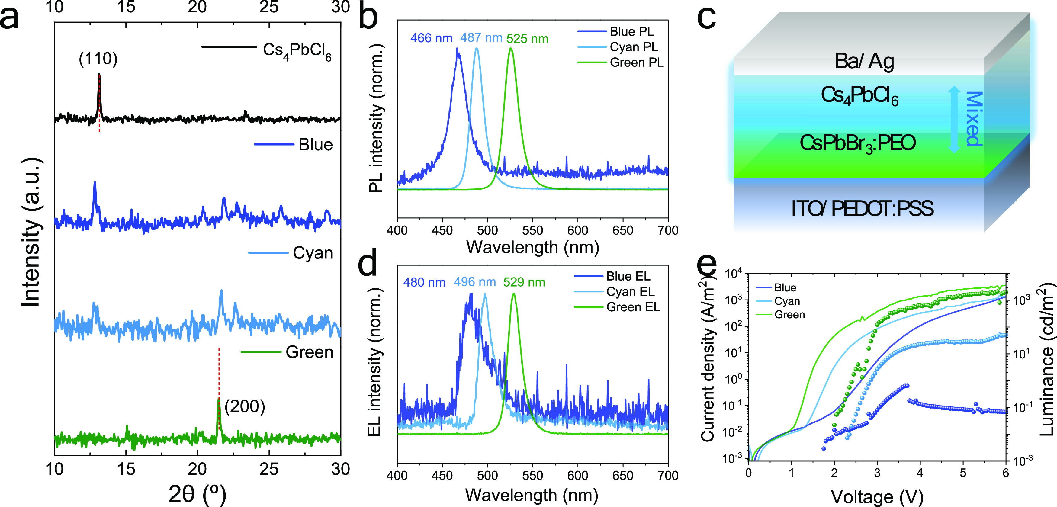
(a) XRD patterns of CsPbBr3, Cs4PbCl6, and mixed-halide films obtained by diffusion between them. (b) PL spectra of green-emissive CsPbBr3, mixed cyan, and blue-emitting films. (c) Schematic illustration and (d) EL and (e) J–V–L data of the light emitters based on the pristine and mixed perovskites.
The PL spectra of the CsPbBr3, CsPbBr3/Cs4PbCl6 (25 nm), and CsPbBr3/Cs4PbCl6 (50 nm) films show sharp and symmetric peaks centered at 525 (green), 487 (cyan), and 466 nm (blue), respectively (Figure 4b). Thus, by controlling anion intermixing through the material dimensionality (3D/0D) and the thickness of the 0D film, it is possible to fine tune the emission of the perovskite heterojunction. Interestingly, the PL quantum yield (PLQY) of the three materials do not follow a monotonic trend, with the cyan emitter having more efficient PL (14.0%) as compared to the green (9.5%) and blue (3.6%) materials. The same set of materials were incorporated in thin-film LEDs with the structure depicted in Figure 4c, where the perovskites are sandwiched between an ITO/PEDOT:PSS anode and a Ba/Ag cathode. The Ba layer is employed to ensure ohmic electron injection, similar to previous reports where LiF interlayers were used.18,19 We note that the blue emitter is not operational without the Ba layer. As shown in Figure 4d, the EL spectra for the three materials are only slightly red-shifted as compared to their corresponding PL. The JVL curves for three representative devices are reported in Figure 4e. The maximum measured luminance values were 2000 and 100 cd/m2 for green and cyan emitters, respectively, which is comparable to other recent reports on similar CsPbX3:PEO perovskite emitters.13,18,19 We observed a low current density and luminance for the blue emitter, which might be related with the thick insulating Cs4PbX6 0D top layer. In general, the current efficiency during J–V scan was found to be relatively low (<1 cd/A, Supporting Information, Figure S7).
Conclusions
In summary, perovskite heterojunctions were successfully fabricated by subsequent solution-process and vacuum co-evaporation. The halide mixing properties of 3D/3D and 3D/0D bilayers were evaluated, and we found that the CsPbBr3/Cs4PbCl6 heterojunction showed limited anion intermixing, leading to a structurally stable 3D/0D interface. These heterostructures can be exploited in light-emitters, where the triple-layer 0D/3D/0D heterojunction was found to be more efficient and stable as compared to the 3D/0D or 0D/3D bilayers. Also, we achieved fast response, electron transport layer-free CsPbBr3 light emitters with reasonable luminance compared to recent reports, without adding any ionic salt. This work proposes a way to stabilize or even suppress anion intermixing at the perovskite heterojunction, which is relevant for the future development of perovskite LEDs. Additionally, we also showed that in these bilayers, it is possible to promote halide mixing when the bilayers are exposed to solvent vapor. Using this method, the photo- and electroluminescence can be tuned from green to blue by adjusting the thickness of the 0D Cs4PbCl6 top layer.
Experimental Section
Materials
Cesium bromide (CsBr, 99.9%) is purchased from Alfa Aesar, and lead bromide (PbBr2, 98%), cesium chloride (CsCl, 99.999%), polyethylene oxide (PEO, Mw ≈ 600,000), and dimethylsulfoxide (DMSO, anhydrous) are purchased from Sigma Aldrich. Lead chloride (99.999%) is purchased from Lumtec. Poly(3,4-ethylenedioxythiophene) polystyrene sulfonate (PEDOT:PSS, AI 4083) is purchased from Clevios.
Preparation
Indium tin oxide (ITO) substrate (3 cm × 3 cm) is cleaned with detergent, tap water, deionized water, and isopropanol for 5 min, and this substrate is treated in UV ozone for 20 min before the spin-coating of PEDOT:PSS (4000 rpm, 30 s). The PEDOT:PSS film is thermally treated with 150 °C 10 min. This film should be cooled-down before the perovskite deposition.
A total of 105 mg of CsBr, 120 mg of PbBr2, and 150 mg of PEO are mixed in 8 mL of DMSO and stirred at 50 °C overnight. The solution was cooled down before spin-coating (1000 rpm 60 s in a N2 glovebox) on the PEDOT:PSS film. Right after spin-coating, the sample is transferred into the antechamber of the glovebox and vacuum-treated for 90 s. Finally, the perovskite film is annealed at 70 °C on a hot plate for 3 min.
For the subsequent deposition of the cesium lead chloride films, the CsPbBr3 perovskite film is transferred into a second glove box with an integrated vacuum chamber. The precursors are thermally evaporated in a chamber (custom made by Thermal Vacuum Projects) with a base pressure of 10–6 mbar. The deposition rate for PbCl2 is kept constant at 0.5 Ȧ/s, while the deposition rates used for CsCl were 1.7 and 0.4 Ȧ/s for Cs4PbCl6 and CsPbCl3, respectively. A calibration factor was obtained by comparing the thickness inferred from the quartz crystal microbalance (QCM) sensors with that measured with a mechanical profilometer (Ambios XP1).
Characterization
Absorption spectra were collected using a fiber optics-based Avantes, Avaspec2048 spectrometer. The photoluminescence spectra were also measured with an Avantes, Avaspec2048 spectrometer, and films were illuminated with a diode laser of integrated optics, emitting at 375 nm. The crystalline structure of the film samples was studied by XRD. The patterns were collected in Bragg–Brentano geometry on an Empyrean PANalytical powder diffractometer with a copper anode operated at 45 kV and 40 mA. Further analysis, including Le Bail fits, was performed with Fullprof software. The devices were measured by applying a constant current density of 100 A/m2 while monitoring the voltage and luminance versus time.
Supporting Information Available
The Supporting Information is available free of charge at https://pubs.acs.org/doi/10.1021/acsphotonics.2c00604.
Band diagrams, supplementary electrical characterization, complementary optical absorption, photoluminescence, electroluminescence (PDF)
This project has received funding from the European Research Council (ERC) under the European Union’s Horizon 2020 research and innovation program (grant agreement no. 834431), from the Comunitat Valenciana (PROMETEU/2020/077) and from grants CEX2019-000919-M and PDC2021-121317-I00 project funded by MCIN/AEI/10.13039/501100011033 and the European Union “NextGenerationEU”/PRTR”. M.S. and F.P. acknowledge funding by MCIN/AEI/10.13039/501100011033 and by “ESF Investing in your future” for their grants RYC-2016-21316 and IJC2018-036753-I, respectively.
The authors declare no competing financial interest.
Supplementary Material
References
- Poyiatzis N.; Athanasiou M.; Bai J.; Gong Y.; Wang T. Monolithically Integrated White Light LEDs on (11–22) Semi-Polar GaN Templates. Sci. Rep. 2019, 9, 1383. 10.1038/s41598-018-37008-5. [DOI] [PMC free article] [PubMed] [Google Scholar]
- Geisz J. F.; France R. M.; Schulte K. L.; Steiner M. A.; Norman A. G.; Guthrey H. L.; Young M. R.; Song T.; Moriarty T. Six-Junction III–V Solar Cells with 47. 1% Conversion Efficiency under 143 Suns Concentration. Nat. Energy 2020, 5, 326–335. 10.1038/s41560-020-0598-5. [DOI] [Google Scholar]
- Aho A.; Isoaho R.; Raappana M.; Aho T.; Anttola E.; Lyytikäinen J.; Hietalahti A.; Polojärvi V.; Tukiainen A.; Reuna J.; Peltomaa L.; Guina M. Wide Spectral Coverage (0.7–2.2 EV) Lattice-Matched Multijunction Solar Cells Based on AlGaInP, AlGaAs and GaInNAsSb Materials. Progr. Photovolt.: Res. Appl. 2021, 29, 869–875. 10.1002/pip.3412. [DOI] [Google Scholar]
- Clark C. P.; Mann J. E.; Bangsund J. S.; Hsu W.-J.; Aydil E. S.; Holmes R. J. Formation of Stable Metal Halide Perovskite/Perovskite Heterojunctions. ACS Energy Lett. 2020, 5, 3443–3451. 10.1021/acsenergylett.0c01609. [DOI] [Google Scholar]
- Kang D.-H.; Kim S.-G.; Kim Y. C.; Han I. T.; Jang H. J.; Lee J. Y.; Park N.-G. CsPbBr 3 /CH 3 NH 3 PbCl 3 Double Layer Enhances Efficiency and Lifetime of Perovskite Light-Emitting Diodes. ACS Energy Lett. 2020, 2191–2199. 10.1021/acsenergylett.0c01036. [DOI] [Google Scholar]
- Shi E.; Yuan B.; Shiring S. B.; Gao Y.; Akriti; Guo Y.; Su C.; Lai M.; Yang P.; Kong J.; Savoie B. M.; Yu Y.; Dou L. Two-Dimensional Halide Perovskite Lateral Epitaxial Heterostructures. Nature 2020, 580, 614–620. 10.1038/s41586-020-2219-7. [DOI] [PubMed] [Google Scholar]
- Elmelund T.; Scheidt R. A.; Seger B.; Kamat P. V. Bidirectional Halide Ion Exchange in Paired Lead Halide Perovskite Films with Thermal Activation. ACS Energy Lett. 2019, 4, 1961–1969. 10.1021/acsenergylett.9b01280. [DOI] [Google Scholar]
- Fakharuddin A.; Gangishetty M. K.; Abdi-Jalebi M.; Chin S.-H.; bin Mohd Yusoff A. R.; Congreve D. N.; Tress W.; Deschler F.; Vasilopoulou M.; Bolink H. J. Perovskite Light-Emitting Diodes. Nat. Electron. 2022, 5, 203–216. 10.1038/s41928-022-00745-7. [DOI] [Google Scholar]
- Akkerman Q. A.; Park S.; Radicchi E.; Nunzi F.; Mosconi E.; De Angelis F.; Brescia R.; Rastogi P.; Prato M.; Manna L. Nearly Monodisperse Insulator Cs4PbX6 (X = Cl, Br, I) Nanocrystals, Their Mixed Halide Compositions, and Their Transformation into CsPbX3 Nanocrystals. Nano Lett. 2017, 17, 1924–1930. 10.1021/acs.nanolett.6b05262. [DOI] [PMC free article] [PubMed] [Google Scholar]
- De Matteis F.; Vitale F.; Privitera S.; Ciotta E.; Pizzoferrato R.; Generosi A.; Paci B.; Di Mario L.; Cresi J. S. P.; Martelli F.; Prosposito P. Optical Characterization of Cesium Lead Bromide Perovskites. Crystals 2019, 9, 280. 10.3390/cryst9060280. [DOI] [Google Scholar]
- Li J.; Du P.; Li S.; Liu J.; Zhu M.; Tan Z.; Hu M.; Luo J.; Guo D.; Ma L.; Nie Z.; Ma Y.; Gao L.; Niu G.; Tang J. High-Throughput Combinatorial Optimizations of Perovskite Light-Emitting Diodes Based on All-Vacuum Deposition. Adv. Funct. Mater. 2019, 29, 1903607. 10.1002/adfm.201903607. [DOI] [Google Scholar]
- Du P.; Li J.; Wang L.; Liu J.; Li S.; Liu N.; Li Y.; Zhang M.; Gao L.; Ma Y.; Tang J. Vacuum-Deposited Blue Inorganic Perovskite Light-Emitting Diodes. ACS Appl. Mater. Interfaces 2019, 11, 47083–47090. 10.1021/acsami.9b17164. [DOI] [PubMed] [Google Scholar]
- Liashenko T. G.; Pushkarev A. P.; Naujokaitis A.; Pakštas V.; Franckevičius M.; Zakhidov A. A.; Makarov S. V. Suppression of Electric Field-Induced Segregation in Sky-Blue Perovskite Light-Emitting Electrochemical Cells. Nanomaterials 2020, 10, 1937. 10.3390/nano10101937. [DOI] [PMC free article] [PubMed] [Google Scholar]
- Ávila J.; Momblona C.; Boix P. P.; Sessolo M.; Bolink H. J. Vapor-Deposited Perovskites: The Route to High-Performance Solar Cell Production?. Joule 2017, 1, 431–442. 10.1016/j.joule.2017.07.014. [DOI] [Google Scholar]
- Song L.; Guo X.; Hu Y.; Lv Y.; Lin J.; Liu Z.; Fan Y.; Liu X. Efficient Inorganic Perovskite Light-Emitting Diodes with Polyethylene Glycol Passivated Ultrathin CsPbBr3 Films. J. Phys. Chem. Lett. 2017, 8, 4148–4154. 10.1021/acs.jpclett.7b01733. [DOI] [PubMed] [Google Scholar]
- Chin S. H.; Choi J. W.; Hu Z.; Mardegan L.; Sessolo M.; Bolink H. J. Tunable Luminescent Lead Bromide Complexes. J. Mater. Chem. C 2020, 8, 15996–16000. 10.1039/d0tc04057f. [DOI] [Google Scholar]
- Alahbakhshi M.; Mishra A.; Haroldson R.; Ishteev A.; Moon J.; Gu Q.; Slinker J. D.; Zakhidov A. A. Bright and Effectual Perovskite Light-Emitting Electrochemical Cells Leveraging Ionic Additives. ACS Energy Lett. 2019, 4, 2922–2928. 10.1021/acsenergylett.9b01925. [DOI] [Google Scholar]
- Mishra A.; Alahbakhshi M.; Haroldson R.; Bastatas L. D.; Gu Q.; Zakhidov A. A.; Slinker J. D. Enhanced Operational Stability of Perovskite Light-Emitting Electrochemical Cells Leveraging Ionic Additives. Adv. Opt. Mater. 2020, 8, 2000226. 10.1002/adom.202000226. [DOI] [Google Scholar]
- Mishra A.; Alahbakhshi M.; Haroldson R.; Gu Q.; Zakhidov A. A.; Slinker J. D. Pure Blue Electroluminescence by Differentiated Ion Motion in a Single Layer Perovskite Device. Adv. Funct. Mater. 2021, 31, 2102006. 10.1002/adfm.202102006. [DOI] [Google Scholar]
- Protesescu L.; Yakunin S.; Bodnarchuk M. I.; Krieg F.; Caputo R.; Hendon C. H.; Yang R. X.; Walsh A.; Kovalenko M. V. Nanocrystals of Cesium Lead Halide Perovskites (CsPbX3, X = Cl, Br, and I): Novel Optoelectronic Materials Showing Bright Emission with Wide Color Gamut. Nano Lett. 2015, 15, 3692–3696. 10.1021/nl5048779. [DOI] [PMC free article] [PubMed] [Google Scholar]
- Thumu U.; Piotrowski M.; Owens-Baird B.; Kolen’ko Y. V. Zero-Dimensional Cesium Lead Halide Perovskites: Phase Transformations, Hybrid Structures, and Applications. J. Solid State Chem. 2019, 271, 361–377. 10.1016/j.jssc.2019.01.005. [DOI] [Google Scholar]
- Shen Z.; Song P.; Qiao B.; Cao J.; Bai Q.; Song D.; Xu Z.; Zhao S.; Zhang G.; Wu Y. Impeding Anion Exchange to Improve Composition Stability of CsPbX 3 (X = Cl, Br) Nanocrystals through Facilely Fabricated Cs4Pb X 6 Shell. Chinese Phys. B 2019, 28, 086102 10.1088/1674-1056/28/8/086102. [DOI] [Google Scholar]
- Karlsson M.; Yi Z.; Reichert S.; Luo X.; Lin W.; Zhang Z.; Bao C.; Zhang R.; Bai S.; Zheng G.; Teng P.; Duan L.; Lu Y.; Zheng K.; Pullerits T.; Deibel C.; Xu W.; Friend R.; Gao F. Mixed Halide Perovskites for Spectrally Stable and High-Efficiency Blue Light-Emitting Diodes. Nat. Commun. 2021, 12, 361. 10.1038/s41467-020-20582-6. [DOI] [PMC free article] [PubMed] [Google Scholar]
- Ren Z.; Xiao X.; Ma R.; Lin H.; Wang K.; Sun X. W.; Choy W. C. H. Hole Transport Bilayer Structure for Quasi-2D Perovskite Based Blue Light-Emitting Diodes with High Brightness and Good Spectral Stability. Adv. Funct. Mater. 2019, 29, 1905339. 10.1002/adfm.201905339. [DOI] [Google Scholar]
- Qian X.-Y.; Tang Y.-Y.; Zhou W.; Shen Y.; Guo M.-L.; Li Y.-Q.; Tang J.-X. Strategies to Improve Luminescence Efficiency and Stability of Blue Perovskite Light-Emitting Devices. Small Sci. 2021, 1, 2000048. 10.1002/smsc.202000048. [DOI] [Google Scholar]
- Chin S. H.; Choi J. W.; Woo H. C.; Kim J. H.; Lee H. S.; Lee C. L. Realizing a Highly Luminescent Perovskite Thin Film by Controlling the Grain Size and Crystallinity through Solvent Vapour Annealing. Nanoscale 2019, 11, 5861–5867. 10.1039/C8NR09947B. [DOI] [PubMed] [Google Scholar]
Associated Data
This section collects any data citations, data availability statements, or supplementary materials included in this article.


