Abstract
Wireless battery-free optogenetic devices enable behavioral neuroscience studies in groups of animals with minimal interference to natural behavior. Real-time independent control of optogenetic stimulation through near-field communication dramatically expands the realm of applications of these devices in broad contexts of neuroscience research. Dissemination of these tools with advanced functionalities to the neuroscience community requires protocols for device manufacturing and experimental implementation. This protocol describes detailed procedures for fabrication, encapsulation, and implantation of recently developed advanced wireless devices in head mounted and back mounted forms. In addition, procedures for standard implementation of experimental systems in mice are provided. This protocol aims to facilitate the application of wireless optogenetic devices in advanced optogenetic experiments involving groups of freely moving rodents and complex environmental designs. The entire protocol lasts about three to five weeks.
Editorial summary
Detailed procedures to fabricate, encapsulate, and implant advanced wireless battery-free devices in head mounted and back mounted forms, to facilitate optogenetic experiments in freely moving rodents.
Introduction
Recently developed wireless optogenetic devices1,2,3,4,5 enable promising applications in neuroscience research by eliminating steric constraints introduced by traditional wired systems, such as optical fibers6,7. These devices support light stimulation through microscale inorganic light emitting diodes (μ-ILEDs) to modulate local activity in neurons expressing light-sensitive opsins, for example Channelrhodopsin (ChR2)8,9,10,11. Previous studies have illustrated the fabrication and application of wireless multimodal optogenetic and optofluidic devices3,12. However, these devices employ bulky and heavy head stages that increase fabrication complexity and affect the animals’ natural behavior. Therefore, the development of miniaturized battery-free wireless head mounted (HM) platforms is essential to further reduce physical constraints and device weight. Recent accomplishments involve using resonant magnetic inductive coupling at radio frequency (RF) to replace the battery, allowing full subdermal implantation on top of the skull1,10,13. Furthermore, to overcome power limitations imposed by the small footprint of the HM platform, we have developed an alternative geometry, where the electronic module containing the receiving antenna and electronic components rests on the animal’s back. The back mounted (BM) electronic module connects to brain-implanted probes with soft and stretchable traces along the spine, enabling advanced functions, stronger illumination, and peripheral nerve stimulation8.
Recently developed HM and BM platforms support non-deterministic real-time control over multi-channel optical stimulation for the first time, by incorporating near-field communication (NFC) and microcontroller operation14. This new functionality significantly expands the experimental context available for optogenetic studies using wireless devices. For example, multi-channel operations can be leveraged to independently control several brain regions over individual subjects in the same arena, with the capacity to update stimulation parameters in real-time conditional on behavioral observations or performance of a specific action14.
Although the development of these wireless multilateral devices offers promising applications in neuroscience studies, detailed protocols to guide the community to fabricate and apply these devices according to their experimental requirements are currently lacking. Previous efforts have introduced only the general fabrication process of battery-free wireless power systems1 with pre-programmed operation parameters10 in HM form factors. Here, we extend the scope by presenting a comprehensive protocol that covers fabrication, chip programming, and surgical implantation of HM and BM optogenetic devices. These improved devices offer synchronized bilateral stimulation, and also achieve real-time control of up to four μ-ILED channels over four stimulation parameters—intensity, frequency, duty cycle, and operation mode. Each channel can be individually selected and programmed wirelessly in the course of the experiment using standardized international NFC protocols. We also provide an open-source graphic user interface (GUI) that allows seamless interfacing between users’ control software and commercial NFC reader/writer to implement a broad range of optogenetics stimulation capabilities. In addition, we include detailed guidance on establishing and operating the experimental systems for optogenetic studies in freely moving animals.
Development of wireless battery-free optogenetic devices and comparison with prior art
Traditional light delivery methods for in vivo optogenetic studies in rodents utilize optical fibers. One downside of these techniques is reduced mobility due to tethering by the coupled optical cables15. This physical constraint impedes neuroscientists from fully exploring the neural encoding of animals’ naturalistic behavior. To address this concern, conventional optogenetic studies habituate animals to the fiber optic system for numerous days prior to behavioral assessment, reducing the effects of tethering on behaviors16,17. Habituation may lower the likelihood of confounding behavioral variables or stress associated with tethering, but it necessarily extends the duration of time before data collection, posing a risk to time-sensitive experiments. Our previous work has reported HM and BM battery-free wireless platforms that eliminate the tethering constraint and provide advanced functions for behavioral studies14. This protocol began as an extension of that work and our other previously reported protocols3,12, in order to guide the neuroscience community to fabricate and employ these devices according to experimental requirements. In general, the upgrade in electronic functions requires a larger device platform and more electronic components. For optogenetic studies that need synchronized bilateral stimulation, passive HM bilateral devices provide this type of stimulation with intensity, frequency, and duty cycle controlled by the RF primary antenna wrapped around the experimental enclosure. For studies that require complex controls, further implementation of NFC components with a microcontroller can change illumination parameters over multiple μ-ILED channels in real-time (active HM device). BM devices demonstrate the design concept of separating the electronic module and probes, to break spatial restrictions imposed by the HM platform. Circuit and electronic components are located on the animal’s back as there is space for a larger receiving coil antenna and more electronic components. However, the connection between circuit and probes must stay intact after contortions induced by animal’s natural movement. For example, in mice, a common model in neuroscience research, deformation ranging from ~30% compression to ~60% elongation is common at the neck region, where connection traces reside14. Here, we apply photolithographically patterned serpentine metal traces bonded on a flexible elastomer to support sustainable electronic connections during such extensive deformation.
Applications of the protocol
This protocol focuses on the fabrication and implantation procedures for HM and BM devices for optogenetic neural control in rodents. The fabrication procedure for HM devices involves flexible printed circuit board processing using laser ablation, soldering, and firmware programming, which can be adjusted to geometrical design and electronic functions that satisfy different application requirements. The fabrication procedure of the BM devices requires additional photolithography. The same principles can be further applied to any devices that require physical separation between stimulation sites and electronic components. The implantation procedures described here for both HM and BM devices can be further applied to other wireless devices that share similar form factors.
Expertise needed to implement the protocol
The fabrication of devices with special configuration, e.g., serpentine thin film connectors on flexible elastomer supports, requires cleanroom facilities. Application of these fabrication procedures requires special trained expertise in standard microfabrication which involves thin film deposition, dry/wet etching, and photolithography. Most universities and research institutes offer cleanroom facilities and training programs necessary for new users to complete this protocol. The implantation of devices requires an animal husbandry facility, and personnel on corresponding protocols, approved by their local Animal Care and Use Committee. This protocol can be carried out by separate trained individuals responsible for device fabrication and animal preparation.
Limitations
The use of wireless stimulation devices allows animals to behave freely, without the physical burden or restrictions associated with external tethering. Additionally, a full subdermal wireless application increases the likelihood of retaining group social housing during the length of the experiment, as there is no external equipment that a cage mate can disturb. However, interactions among animals in a group can cause wound dehiscence along the sutures, which may dislodge both the HM and BM devices. Thus, researchers need to be cognizant of this and develop appropriate monitoring procedures for paradigms that require continued social interactions, especially in the early stages of surgical recovery. The developed biocompatible encapsulation process, together with careful handling during device assembly and implantation, allows these devices to operate over 9 weeks (the longest tested period), which satisfies most behavioral neuroscience requirements for experiments involving small rodents14. The BM platform offers promising future applications in studies that require optogenetic stimulation in combination with real-time sensing capabilities, which is not covered in this protocol. The implementation of low frequency sensing, e.g. <10 samples per second, can be straightforwardly implemented using this device architecture together with a joint firmware/hardware upgrade. The sensing of high frequency physiological signals, however, requires the integration of Bluetooth low energy (BLE) chip that supports large bandwidth data transmission with specialized sensors (electroencephalogram, mechano-acoustic, near infrared spectroscopy, myocardiogram, etc) with high fidelity. Furthermore, adding real-time controllable drug delivery capability will further enhance multimodal control over neural activity and other organ function. Building such advanced device platforms remains challenging from current engineering perspectives, but it is expected to be achieved in the near future.
Experimental design
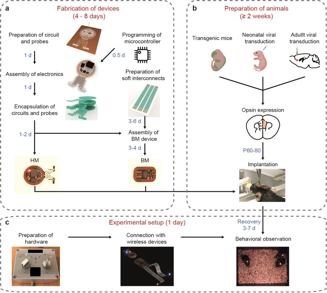
In the procedure, we include fabrication, implantation, and application procedures for passive HM devices that offer synchronized bilateral stimulations, as well as active HM and BM devices with NFC communication that enable real-time control over stimulation parameters using two and four μ-ILEDs respectively. Researchers can choose the design based on experimental requirements. Not all parts of the procedure need to be undertaken for all devices. For fabrication of passive HM devices, follow steps 1–5 and 27–33. For fabrication of active HM devices, follow steps 1–8 and 27–33. For fabrication of BM devices, follow steps 1–32 and 34–42. Figure 1 is a flow chart overviewing the main parts of the procedure.
Figure 1: Flowchart of general procedures.
a, Steps of device fabrication. b, Steps of animal preparation. c, Steps of experimental setup.
Subjects:
The dimensions of the HM and BM devices in this protocol were optimized for adult C57BL/6J mice in both sexes but are expected to fit other mouse strains and rodents in the 20–40 g size range. Future stimulation devices will accommodate larger animals, such as rats and squirrel monkeys. Following implantation, animals do not require special housing and should have free access to environment enrichment, food, and water, as required or advised by the institution. Before beginning this protocol, all the procedures described should be approved by the institutional Animal Care and Use Committee.
Cost:
The estimated total expense for the materials required to implement this protocol in the USA is uploaded at the link https://doi.org/10.5281/zenodo.5592873 18.
Controls:
Experiments should have proper controls to account for changes in behavior resulting from virus administration or device implantation. Animals expressing a genetically encoded opsin should be observed within the experimental setting without optogenetic stimulation prior to experiments. Control animals should be transduced with a fluorescent reporter to exclude any confounding factors introduced by virus administration or μ-ILED activation. Control animals should undergo the same optical stimulation paradigms to control for any thermal effects of the μ-ILEDs19.
Real-time control over stimulation parameters
Active HM and BM devices with NFC communication capability expand the range of possible stimulation protocols for optogenetic studies. Thus, researchers are free to independently control up to four channels (μ-ILEDs) in real-time during experiments. Independently tunable parameters for each channel include ON-OFF status, stimulation frequency, pulse width, programable burst stimulation, and light intensity control. With a customized user interface, or a software library, researchers can design complex optogenetic protocols that satisfy the needs of diverse behavioral experiments. Moreover, these tools open the possibility to explore more complex stimulating strategies for advanced behavioral studies, including synchronized/desynchronized stimulation of multiple brain regions in one subject, switchable excitation/inhibition of the same brain region, individualized stimulation of multiple subjects within the same behavioral test apparatus, as well as real-time switching and closed-loop control of stimulation protocols.
Materials
Biological materials
Mice. We have successfully used C57BL/6 mice (Charles River Laboratories, Wilmington, MA) Caution! Any experiments involving live animals must conform to relevant Institutional and national regulations. All procedures described here were approved by the Animal Care and Use Committee of Northwestern University and conform to the US National Institutes of Health guidelines.
AAV1-CaMKIIa-hChR2(H134R)-mCherry (Addgene, 26975-AAV1)
Reagents
Preparation of electronic modules and probes
Commercial surface mounted electronic components including capacitors (Digikey, 712–1465-ND), resistors (Digikey, KIT-RMCF0201FT-03-ND, KIT-RMCF0201FT-05-ND), low dropout regulators (2.8V; Digikey, NCP161AMX280TBG, NCP161BFCS280T2G), and Schottky diodes (Digikey, RB751S-40DP-TP).
Stainless steel flux (Grainger, 23171534)
Conductive silver paint (TED PELLA Inc., 16040–30).
Flexible copper–polyimide-copper (18, 75 and 18 μm; Dupont, Pyralux AP8535R).
Isopropyl alcohol (Sigma Aldrich, PX180). Caution! Isopropyl alcohol is flammable.
Low temperature solder pastes (ChipQuik, SMDLTLFP10T5).
Micro inorganic light emitting diodes (μ-ILEDs; CREE Inc., TR2227 for emission at 460 nm and 535 nm; III-V Compounds, TCE 12 for emission at 590 nm and 630 nm), matched to opsin excitation wavelengths20.
NFC chip (ST Microelectronic, M24LR16E).
Operational amplifier (Texas Instruments, TLV8542).
Programming of microcontroller
Commercial programmer (SparkFun, PGM-11801).
Flexible electrical wires.
Micro-controller, QFN20 4 mm × 4 mm packaging (Microchip Technology, ATtiny 84).
QFN20 socket, 0.5 pitch and 4 mm × 4 mm chip size, to DIP20 adapter (Plastronics, 20QN50S14040).
Arduino IDE open-source software (V1.18.15 or later).
Preparations of soft interconnections
CRITICAL Certain reagents in this section require use and storage in a cleanroom, marked as “Cleanroom chemical”.
4-inch silicon wafer (University Wafers, S4P01SP).
Acetone (Sigma Aldrich, 179124). Caution! Acetone is flammable.
Buffered oxide etch (BOE 6:1; Avantor). Caution! BOE is extremely toxic and corrosive and should be used in appropriately ventilated fume hood. Cleanroom chemical.
Copper etchant (Transene Inc., Type CE-100). Cleanroom chemical.
Developer (Microchemicals, AZ 400K). Cleanroom chemical.
Gold etchant (Transene Inc., Type TFA). Cleanroom chemical.
Parylene (Special Coating Systems, Parylene C). Cleanroom chemical.
Photoresist (Kayaku Adv Materials, S1813; and Integrated Micro Materials, AZ 4620). Cleanroom chemical.
Poly(methyl methacrylate) (PMMA; MicroChem, 495PMMA A8). Caution! PMMA is flammable and should be used in a well-ventilated space. Cleanroom chemical.
Silicone elastomer (Ecoflex 00–30, SMOOTH-ON).
Water soluble tape (AQASOL, ASWT-1).
Encapsulation of electronic modules and probes
50 μm tungsten sheet (Sigma Aldrich, 267538).
Epoxy superglue (DEVCON, 31345 2 ton clear epoxy).
Polydimethylsiloxane (PDMS; Dow Corning, Sylgard 184).
Assembly of back mounted devices
75 μm polyimide sheet (PI; Argon Masking Inc., PC533FILM-8000–36).
Polyimide tape (Kapton, KPT2–1/4).
Equipment
Fabrication of devices
CRITICAL Certain equipment in this section requires use and storage in a cleanroom, marked as “Cleanroom facility”.
Chemical vapor deposition (Special Coating Systems; Labcoter PDS 2010) for parylene coating. Cleanroom facility.
Electron beam vapor deposition (AJA International, ATC-2030-E HV) for Ti, Cu, and Au thin film deposition. Cleanroom facility.
Hot air soldering station (Sumsour, 8586).
Impedance analyzer (Keysight, E4900A).
Maskless aligner (Heidelberg, MLA150). Cleanroom facility.
Protolaser (LPKF Laser & Electronics, ProtoLaser U4).
Reactive-ion etching (Samco Inc., RIE-10NR; and March, CS-1701). Cleanroom facility.
Sonicator bath (Branson, CPX952139R).
Spin coater (Brewer Science, 200X; and Laurell Technologies Corporation, WS-650Hz-8NPPB). Cleanroom facility.
Sputter (AJA International, ATC 200) for SiO2 deposition. Cleanroom facility.
Ultraviolet ozone cleaner (Jelight Inc., 144AX).
Virus injection and device implantation
0.9 mm drill bit (Fine Science Tools, 19008–09).
Adhesive activator (Lang Dental, Ortho-Jet BCA Liquid).
Aluminum foil.
Animal temperature controller (Physitemp, TCAT-2LV).
Bead sterilizer (Braintree Scientific, GER 5287–120V).
Curved forceps (Fine Science Tools, 11009–13).
Curved hemostats (Fine Science Tools, 13009–12).
Dental powder (Lang Dental, 1520BLK).
Disposable brushes (Lang Dental, 1900).
Electric clippers (Wahl, 9868).
Fine scissors (Fine Science Tools, 14094–11).
Glass pipette or Hamilton syringe.
Ice boxes.
Isoflurane, USP (Baxter, 1001936040).
Model 1770 standard electrode holder (Kopf, Model 1770).
Needle holders (Fine Science Tools, 12002–12).
Probe clip (Neurolux Inc.).
RC2 rodent circuit controller anesthesia system (Vetequip, 922100).
Rodent ear bars (Kopf 955).
Scalpel handle (Fine Science Tools, 10004–13).
Size 15 blade (Bard Parker, 371153).
Small, curved hemostats (Fine Science Tools,13003–10).
Stereotax alignment system with digital display (Kopf Model 942).
Stereotaxic drill and control box (Foredom, K.107018 or K.1070).
Stereotaxic probe holder (ASI Instruments, PH-300).
Sterile ocular lubricant (Dechra, NDC 17033–211-38).
Straight blunt forceps (Fine Science Tools, 11000–12).
Super glue gel (Loctite, 45440).
3M Transpore™ surgical tape (1527–0, 1/2 inch × 10 yard).
Suture (Ethicon, 8682G).
Syringe needles (Becton Dickson, 328438 and 309626).
UltraMicroPump (UMP3, World Precision Instruments, Sarasota, FL).
Opsin verification
Coverslips (Fisher Scientific, 12–545-MP).
Cryostat (Leica, CM3050S).
Vibratome (Leica, VT1000S)
Dry ice.
Fluorescent microscope (Olympus VS120 or similar).
Forceps (Fisher Scientific, 10–316C).
Glass dish (Fisher Scientific, 08–749F).
Mounting Media (Electron Microscopy Sciences, 17984–24).
Paintbrush (Ted Pella, 11807).
Phosphate Buffered Saline (Thermo Fisher Scientific, 70011044).
Slides (Fisher Scientific, 12–550-15).
Sucrose (Sigma, S7903).
Device operation
Power distribution box (Neurolux Inc.).
Tuner box (Neurolux Inc.).
MATLAB (MathWorks, Matlab R2020b or a more updated version).
Procedure
Preparation of the electronic module and probes • TIMING 1 d
CRITICAL This section includes circuit preparation and electronic component assembly for passive and active HM devices, as well as the probes and module for BM devices. Our previous publication has additional details on these devices and their application14.
-
1
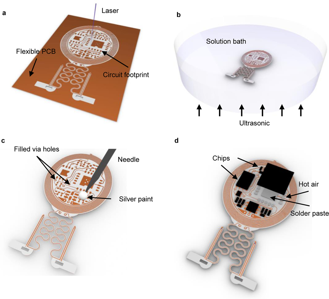
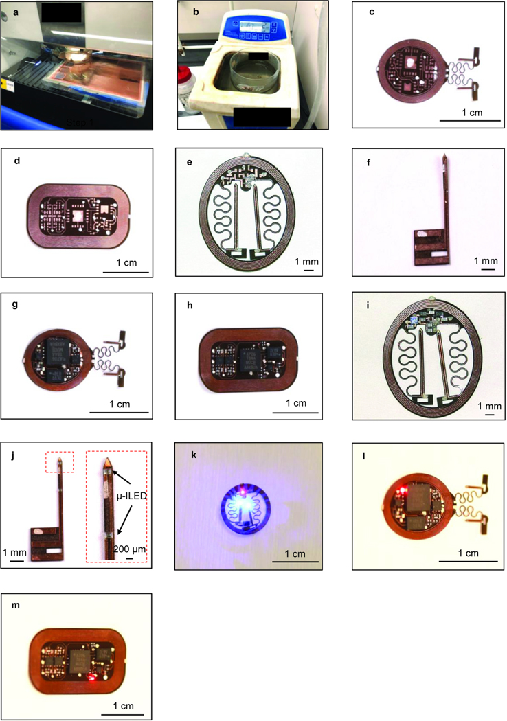
Cut the circuit and probe layout with laser ablation on a flexible copper–polyimide-copper sheet (to dimensions: 18, 75 and 18 μm; Fig. 2a and Extended Data Fig. 1a). Other laser ablation systems can be used as an alternative or flexible printed circuit boards (fPCB) processed by commercial vendors. If fPCB production is outsourced, then skip this step and steps 2 and 3.
Pause point: The process can be paused here. fPCBs can be stored in plastic containers at room temperature for up to one year before the following soldering process.
-
2
Clean the circuit and probe with stainless steel flux solution in a sonicating bath for 2 min (Fig. 2b and Extended Data Fig. 1b). Repeat sonicating process in deionized water for 2 min. Rinse in isopropyl alcohol, and dry with nitrogen gas.
-
3
Fill in all the via holes with conductive silver paint using a 30 gauge blunt needle (Fig. 2c). Start with bottom layer first, make sure the silver paint does not connect with any adjacent vias or traces. Wait 5 min for the paint to dry, turn over the fPCB and proceed with the top side. Wait for 10 mins before attempting to reflow soldering the components. Test continuity using a multimeter to make sure vias electrically connect top and bottom traces (Extended Data Fig. 1c: active HM device; Extended Data Fig. 1d: circuit for BM device; Extended Data Fig. 1e: passive HM device; Extended Data Fig. 1f: probe for BM device).
Critical Step: Proper filling of via holes with the silver paint establishes the electrical connection between the top and bottom copper layers. Thus, make sure the silver paint is still in liquid form when applying it to the via holes.
?Troubleshooting
-
4
Solder all the commercially packaged electronic components onto the fPCB (Fig. 2d), i.e. the capacitors, low dropout voltage regulator, resistors, Schottky diodes, and μ-ILEDs (these components make passive HM devices). For active HM and BM devices, additional soldering of NFC chips, operational amplifiers, and microcontrollers are required. Soldering of microcontrollers should proceed after programming as described in the following steps 6–8. Use low temperature solder and a hot air gun (at a temperature of 250–300 °C; Extended Data Fig. 1g: active HM device; Extended Data Fig. 1h: module for BM device; Extended Data Fig. 1i:passive HM device; Extended Data Fig. 1j: probe for BM device). The AutoCad files for fPCB circuit designs (with component values) of active and passive HM devices, as well as BM devices, are available at ref18.
Critical step: Soldered components require frequent inspections during soldering process as some might not be properly bonded to the copper traces. The resonance of the inductive circuit after soldering the matching capacitor should be inspected with an impedance analyzer to ensure a resonance peak at around 13.56 MHz (radio frequency).
Critical Step: Robust soldering ensures stable connection throughout experiments during animals’ naturalistic activities.
?Troubleshooting
-
5
If assembling a passive HM optogenetics device, assembly finishes here. Check the passive HM device function inside a RF powered cage (Extended Data Fig. 1k) and then proceed to encapsulate the device, as described in step 27. If assembling an active device that is either HM or BM proceed to next step.
?Troubleshooting
Critical Step: After this step, the completion of passive HM device manufacture will take under a week, thus to be able to proceed immediately to device implantation after fabrication is complete, proceed with step 43 (viral transduction of animals) in parallel with the remaining steps of device manufacture.
Pause point: The process can be paused here. Devices can be stored in plastic containers at room temperature for two days at most before encapsulation, starting at step 27.
Figure 2: Schematics of fabrication procedures for head mounted devices.
a, Apply laser ablation to define the circuit footprints and geometrical layouts of head mounted (HM) devices on a flexible double-sided printed circuit board (Cu (18 μm)/PI (75 μm)/Cu (18 μm)). b, Use ultrasonic bath to clean the surface of the HM devices in the stainless steel flux solution. c, Use a 30 gauge blunt needle to dip silver paints through laser-ablated via holes to make electrical connections between top and bottom circuits. d, Use heat gun, 250 °C and low air speed, to melt indium solder pastes and electrically bond the electronic components on circuit footprints.
Programming of microcontroller • TIMING 1 hr
CRITICAL Active HM and BM versions include an NFC chip and an 8-bit AVR microcontroller. This section is only required for active device manufacture.
-
6
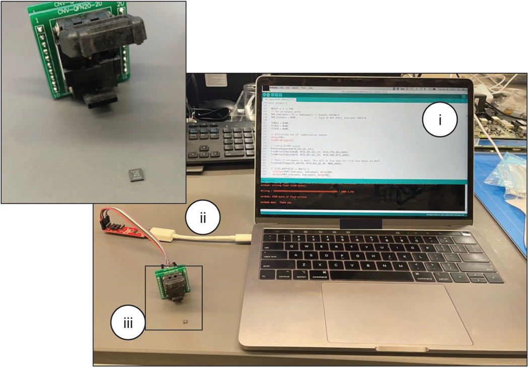
Programmer preparation. Connect the commercial AVR programmer to a QFN20, 0.5 mm pitch, socket for a 4 mm × 4 mm integrated circuit (IC) following the connection schematic shown in Extended Data Fig. 2.
-
7
Programming of microcontroller. Mount the microcontroller to the IC socket. Open the microcontroller chip firmware on Arduino IDE, select the appropriate configuration and download the firmware onto the chip. Follow the open-source programming instructions found here (https://github.com/sparkfun/Tiny-AVR-Programmer/tree/V_1.3).
Critical Step: The microcontroller needs to be programmed with the dedicated optogenetics firmware18.
? Troubleshooting
-
8
Solder the programmed microcontroller onto the fPCB. Check device in the RF antenna. An indicator μ-ILED should flash three times when the device is powered up for the first time (Extended Data Fig. 1l: active HM device; Extended Data Fig. 1m: module for BM device). The microcontroller will initialize the NFC chip when powered up for the first time and initialize the stimulator μ-ILED connected to channel 1 at a frequency of 2 Hz and 50 % duty cycle. If assembling an active HM device, assembly finishes here so proceed to encapsulate the device as described in step 27. If fabricating a BM device, proceed to next step.
Critical Step: This step implements NFC communication for real-time stimulation control.
Critical Step: After this step, the completion of active HM device manufacture will take under a week, thus to be able to proceed immediately to device implantation after fabrication is complete, proceed with step 43 (viral transduction of animals) in parallel with the remaining steps of device manufacture.
Preparation of soft interconnections for back mounted device • TIMING 4–7 d
CRITICAL This section is not required when assembling HM devices. The procedure is applicable to any devices that require physical separation between control electronics and stimulation sites.
CRITICAL Steps 9–17 must be carried out in the cleanroom.
-
9
Degrease the silicon wafer surface sequentially with acetone (~ 20 s), isopropyl alcohol (IPA; ~ 20 s), deionized water (DI; ~ 20 s), and IPA (~ 20 s) using wash bottle with dispensing nozzle and dry with nitrogen gas (~ 1 min). Bake the wafer on a 110 °C hotplate for 1 min to dehydrate. Note that no sonication is required in this step.
-
10
Spin coat PMMA on the silicon wafer (4000 rpm, 500 ramp, 40s, ~ 500 nm), then bake the wafer on 180 °C hotplate for 5 min to cure (Fig. 3a). We use spin coating equipment from Brewer Science in this and the following steps.
CRITICAL STEP: This step forms the sacrificial layer that separates the device from silicon substrate for future transfer printing in step 18.
Pause point: The process can be paused here. Devices can be stored in plastic containers at room temperature for up to one year before the following deposition process.
-
11
Deposit parylene (7 g, ~ 5 μm) through chemical vapor deposition (CVD). We use a system from Special Coating Systems with the following settings: Pyrolisis furnace temperature: 690 °C; Chamber gauge temperature: 135 °C; Vaporizer temperature: 175 °C; Vacuum: 35mT; Operation duration: ~ 2.5 hrs; Fig. 3a.
Pause point: The process can be paused here. Devices can be stored in plastic containers at room temperature for two days at most before the following deposition process.
-
12
Deposit Ti 20 nm (1 Å/s, 200s) / Cu 300 nm (2 Å/s, 1500s) / Ti 20 nm (1 Å/s, 200s)/ Au 50 nm (1 Å/s, 500s) sequentially through electron-beam vapor deposition (Fig. 3a). We use equipment from AJA International for this step.
Critical step: Deposition should operate in high vacuum (pressure below 5E-6 torr) to ensure high deposition quality. The suggested deposition rates prevent overheat of the chamber that could potentially lead to fractures of the thin metal films.
Pause point: The process can be paused here. Devices can be stored in plastic containers at room temperature for two days at most before the following photolithography process.
-
13
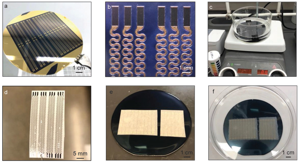
Spin coat (Brewer Science settings: 4000 rpm, 500 ramp, 40s) photoresist (S1813, ~ 1.5 μm thickness, soft bake at 110 °C for 1 min) and pattern serpentine geometry on metal layers through photolithography (Exposure wavelengths: 405 nm; Exposure dose: 80 mJ/cm2; Developer: AZ 400K diluted with water at a volume ratio of 1:4, ~ 45–55 s) and wet chemical etching sequentially with Au etchant (~ 10–15 s), BOE (~ 24–30 s), Cu etchant (~ 5 s) and BOE (~ 24–30 s). Then remove photoresist with acetone rinse (~ 2 min; Fig. 3b and Extended Data Fig. 3a).
Critical step: The Autocad file for serpentine design is uploaded in ref18.
Critical step: We use the maskless aligner from Heidelberg for photolithographical patterning in this and following steps. If using other exposure equipment, parameters for exposure and developing need to be experimentally adjusted. The number of serpentine traces depends on the number of μ-ILED channels. The serpentine geometry determines traces’ stretchability. The electrical resistances of the serpentine traces (~ 44–55 Ω per trace) are measured to evaluate the fabrication quality.
Critical Step: Accurate photolithographical patterning on metal layers yields serpentine traces with desired electrical and mechanical properties. Close attention is required to prevent under or over development, as well as under or over etching during fabrication.
?Troubleshooting
Pause point: The process can be paused here. Devices can be stored in plastic containers at room temperature for one day at most before the following deposition process.
-
14
Repeat step 11 to deposit parylene (7 g, 5 μm) through chemical vapor deposition (Fig. 3c)
Pause point: The process can be paused here. Devices can be stored in plastic containers at room temperature for two days at most before the following deposition process.
-
15
Deposit silicon dioxide (SiO2) with sputter (60 nm). We use equipment from AJA International with the following settings: Pressure: 5 mTorr; Power: 200W; Deposition rate: ~ 0.6 Å/s; Time: ~ 10 min (Fig. 3c).
-
16
Spin coat (Brewer Science settings: 4000 rpm, 500 ramp, 40 s) photoresist (AZ4620, ~ 7 μm thickness, soft bake at 110 °C for 3 min) and pattern serpentine geometry on SiO2 layer through photolithography (Exposure wavelengths: 405 nm, Exposure dose: 200 mJ/cm2, Developer: AZ 400K diluted with water at a volume ratio of 1:2, ~ 45–55 s) followed dry etching with reactive ion etching (RIE; Using Samco Inc. equipment with these settings: CHF3: 20 standard cubic centimeter per minute (sccm), Ar: 10 sccm; Pressure: 1.33 Pa; Power: 100 W; Time:12 min; Fig. 3d).
Critical Step: This step forms the etching mask for the bottom parylene layer. The mask is designed to encapsulate metal serpentine traces with parylene while having the contact pads exposed for electrical connections. Similar to step 13, prevention of under or over development during photolithography, as well as precise control over etching profile (gas composition, power, time) is important to form accurate SiO2 mask for the bottom parylene layer.
-
17
Etch the remaining parylene with RIE (Using March equipment with these settings: O2: 30 sccm; Pressure: 220 mTorr; Power: 200 W; Time: ~ 45 min; Fig. 3e and Extended Data Fig. 3b).
Critical Step: Reserve a 5-minute safety time window during etching process to prevent over etching. Measure the electrical resistance of the serpentine traces on the contact pads with multimeter to indicate the state of etching. If the multimeter displays open circuit, the serpentine traces are still not fully etched. Repeat step 17 with 1-minute etching time intervals until the measured resistances are the same as the measurements in step 13 and the wafer substrate display shiny silicon color without residues.
Critical Step: Similar to step 16, precise control over etching profile, especially etching time, is important to form successful encapsulation over metal traces with contact pads fully exposed for electrical connections.
Pause point: The process can be paused here. Devices can be stored in plastic containers at room temperature for one week at most before the following transfer printing process.
?Troubleshooting
-
18
Transfer printing. Cover the silicon wafer with a thin wipe and another same sized silicon wafer. Clamp the wafers with 2 clips and immerse in 80 °C acetone for 120 mins (Extended Data Fig. 3c).
Critical Step: Complete dissolution of sacrificial layer of PMMA in this step is crucial for future transfer from the current silicon substrate. Sufficient immersion time in acetone should be ensured.
Critical Step: For optimized production efficiency, carry out steps 21–23 in parallel with steps 18–20.
-
19
Extract wafers from acetone and leave for 2 minutes at room temperature for evaporation. Remove the cover and laminate water-soluble tape to the patterned serpentine traces firmly. Gently peel off the water-soluble tape to transfer the traces (Fig. 3f and Extended Data Fig. 3d).
Critical Step: 2-minute evaporation time after taking out wafer from acetone should be strictly followed to allow sufficient liquid evaporation while preventing bonding between serpentine traces and underneath silicon substrate.
-
20
Deposit SiO2 (60 nm) on the serpentine side of the water-soluble tape with sputter using the parameters stated in step 15.
-
21
Meanwhile, prepare another silicon wafer and repeat steps 9–10 to coat PMMA in cleanroom.
Critical step: Spin coated PMMA in this step allows convenient release of future spin coated silicone elastomer (step 23) from silicon substrate.
-
22
Prepare silicone elastomer by mixing Ecoflex (00–30) part A and part B at a ratio of 1:1 wt%.
Critcal step: Proceed to next step within 10 minutes because Ecoflex will cure at room temperature.
-
23
Spin coat Ecoflex (Using Laurell Technologies Corporation equipment with these settings: 400 rpm, 200 ramp, 30 s, ~ 200 μm) on the silicon wafer and cure in a 70 °C convection oven for 2 hrs (Fig. 3g).
-
24
Treat the surface of Ecoflex and SiO2 coated serpentine traces with ultraviolet (UV) light. We use ultraviolet ozone cleaner from Jelight Inc. to expose UV light for 4 minutes.
Critical Step: Proceed immediately to the next step because the UV activation of the surface chemical functionalization for Ecoflex and coated SiO2 for siloxane bonding is temporary.
-
25
Laminate the serpentine traces (on water soluble tape) on the surface of Ecoflex and enhance the internal siloxane bonds by heating in a 70 °C convection oven for 10 mins. (Fig. 3h and Extended Data Fig. 3e).
-
26
Dissolve the water-soluble tape in distilled water (~ 5–10 min) and blow dry the surface with nitrogen gas (~ 2 min, Fig. 3i and Extended Data Fig. 3f). Do not apply sonication in this step.
Pause point: The process can be paused here. Devices can be stored in plastic containers at room temperature for up to one year.
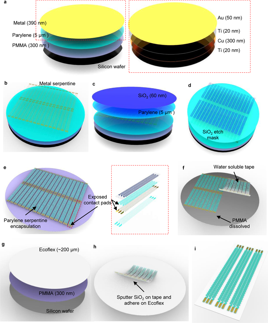
Figure 3: Schematics of fabrication procedures for soft interconnections of back mounted devices.
a, Spin coat polymethyl methacrylate (PMMA, 300 nm) on silicon wafer to form the sacrificial layer. Apply chemical vapor deposition (CVD) process to form a thin layer of parylene (5 μm). Then use electron-beam (E-beam) deposition to form thin metallic layers of Ti (20 nm)/Cu (300 nm)/Ti (20 nm)/Au (50 nm). b, Apply photolithography process followed by wet chemical etching to form serpentine traces on metallic layers. c, Apply CVD process to form another layer of parylene (5 μm). Then use sputter deposition to form a layer of SiO2 (60 nm). d, Apply photolithography process followed by reactive-ion etching (RIE) to form SiO2 etching masks for the underneath parylene layers. The etching masks are defined in serpentine geometries that encapsulate the metallic traces and expose the contact pads for electrical connections. e, Apply RIE process to form parylene serpentine traces defined by SiO2 masks. f, Transfer the interconnection traces from the silicon wafer using water-soluble tapes after dissolving PMMA sacrificial layer with acetone. g, Spin coat PMMA (300 nm) and silicone (Ecoflex, ~ 200 μm). h, Coat SiO2 on water-soluble tape through sputter deposition and adhere the tape on prepared Ecoflex substrate after ultraviolet (UV) treatment. i, Dissolve the water-soluble tape in distilled water and gently blow dry the surface with nitrogen gas.
Encapsulation of the electronic module and probes • TIMING 2–3 d
CRITICAL This section applies to passive and active HM devices, and the probes and electronic module for the BM device. We refer to the probes and electronic module for the BM device as “BM probes” and “BM module”, respectively.
CRITICAL Steps 27–28 and 31–32 must be processed in the cleanroom.
-
27
Clean the surface of the HM devices (passive and active), BM probes and BM module in IPA solution and blow dry with nitrogen gas gun. Do not apply sonication in this step.
Critical Step: Thorough cleaning with IPA and nitrogen gas is extremely important to get rid of dust on the device’s surface before CVD parylene encapsulation. Insufficient cleaning will lead to future encapsulation defects that significantly reduces the device’s operation life in animal after implantation.
Critical Step: Immediately proceed to the next step to avoid contamination of devices after cleaning.
-
28
Coat parylene (20 g, ~ 14 μm) on HM devices (both active and passive), BM probes and BM module through CVD (Fig. 4a). Follow the same operation conditions described in step 11. This is the final step of BM module encapsulation (further assembly of BM devices starts at step 34).
Pause point: The process can be paused here. Devices can be stored in plastic containers at room temperature. The finished BM module can be stored for up to one year before final assembly. Finished HM device and BM probes can be stored for up to one year before the following probe stiffening process.
-
29
Cut the probe stiffeners with the same configuration as probes for HM and BM devices but ~1 −2 mm shorter in length using laser ablation on a 50 μm tungsten sheet.
Critical Step: For probes that are below 2 mm in length, skip this step and steps 30–32.
-
30
Glue the tungsten stiffeners to the back side of the probes (individual BM probes, and probes connected on HM devices) with epoxy superglue (Fig 4b and Extended Data Fig. 4a: active HM device; Extended Data Fig. 4b: passive HM device; Extended Data Fig. 4c: BM probe). Note that the immune responses and gliosis induced by tungsten stiffened probes have been shown to be similar to those caused by conventional optical fibers14. The use of tungsten stiffeners will not affect devices operation longevity as long as these devices are properly encapsulated, as shown in the following steps14.
Critical Step: This step significantly enhances the probe stiffness to prevent deflections during implantation, thus improving the spatial accuracy of light delivery. The ~1–2 mm length difference between the stiffeners and the probes allows bending of the flag after implantation for fixation, as illustrated in step x of section “Device implantation Option A”.
Pause point: The process can be paused here. Devices can be stored in plastic containers at room temperature for up to one year before the following coating process.
-
31
Clean the surface of the BM probes and HM devices in IPA solution and blow dry with nitrogen gas gun. Do not apply sonication in this step.
Critical Step: Similar to step 27, thorough cleaning is extremely important to get rid of dust on the device surface.
Critical Step: Proceed immediately to the next step to avoid contamination of devices after cleaning.
-
32
Coat parylene (20 g, 14 μm) on BM probes and HM devices through chemical vapor deposition (Fig. 4c). Follow the same operation conditions as described in step 28.
Critical Step: After this step, the completion of BM device manufacture will take under a week, thus to be able to proceed immediately to device implantation after fabrication is complete, proceed with step 43 (viral transduction of animals) in parallel with the remaining steps of device manufacture.
Pause point: The process can be paused here. Finished BM probes and HM devices can be stored in plastic containers at room temperature for up to one year before the following coating process.
-
33Coat polydimethylsiloxane (PDMS) on HM devices by undertaking the following :
- Use a tweezer to dip and cover PDMS on probes (~ 0.5 droplet for each) and serpentine connections (~ 0.5 droplet for each) of the device and put the device on a stage to flat coatings for ~ 5–10 min (Fig. 4d).
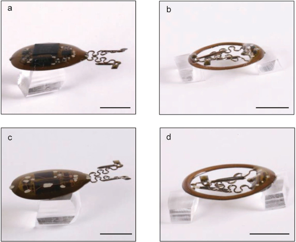
- Use a tweezer to dip and cover PDMS on the coil and electronic components on the top side (~ 6–8 droplets) and put the device on a stage to flatten coatings for 10 min. Then thermally cure the PDMS inside a 70 °C convection oven for another 1 hr (Fig. 4e; Extended Data Fig. 5a – 5b).
- Use a tweezer to dip and cover PDMS on the bottom side (~ 3–4 droplets) of the module followed by the same thermal cure process (Fig. 4f; Extended Data Fig. 5c–5d).
Critical step: This is the final step of fabrication for both active and passive HM devices.
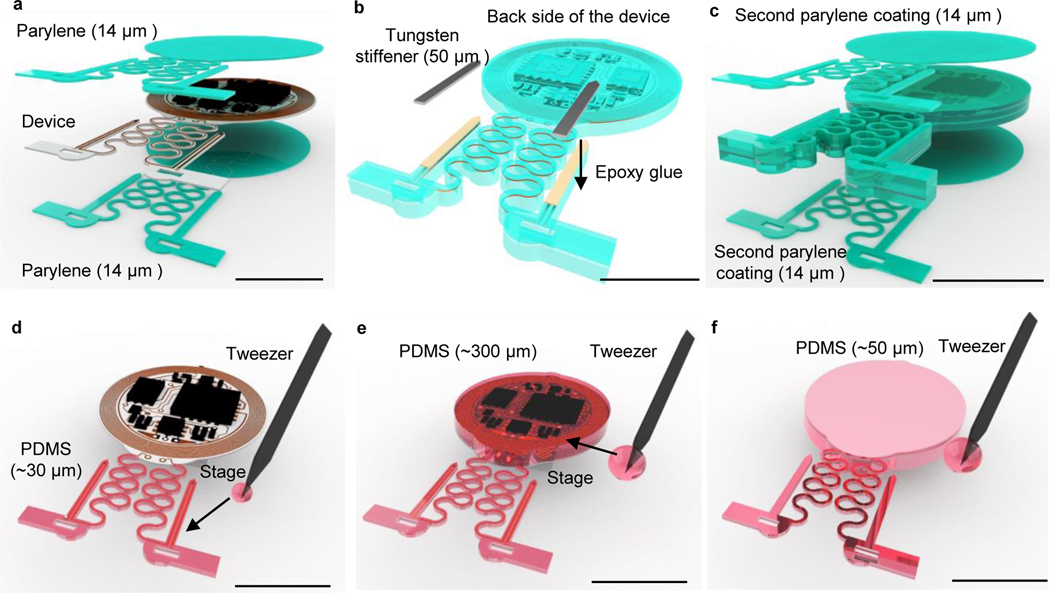
Figure 4: Schematics of encapsulation procedures for head mounted devices.
a, Apply CVD process to form conformal coatings of parylene (14 μm) on the head mounted device. b, Attach tungsten stiffener on to the back side of the probes with epoxy adhesives. c, Apply CVD process to form a second conformal coatings of parylene (14 μm). d, Use a tweezer to dip coat polydimethylsiloxane (PDMS) on serpentine connections and probes. e, Repeat dip coating of PDMS on top side of the device to cover circuits and electronic components followed by thermal curing process. f, Repeat dip coating of PDMS on bottom side of the device followed by thermal curing process. Scale bars: 1 cm.
Assembly of back mounted devices • TIMING 1–2 d
CRITICAL This section applies only to BM devices.
-
6
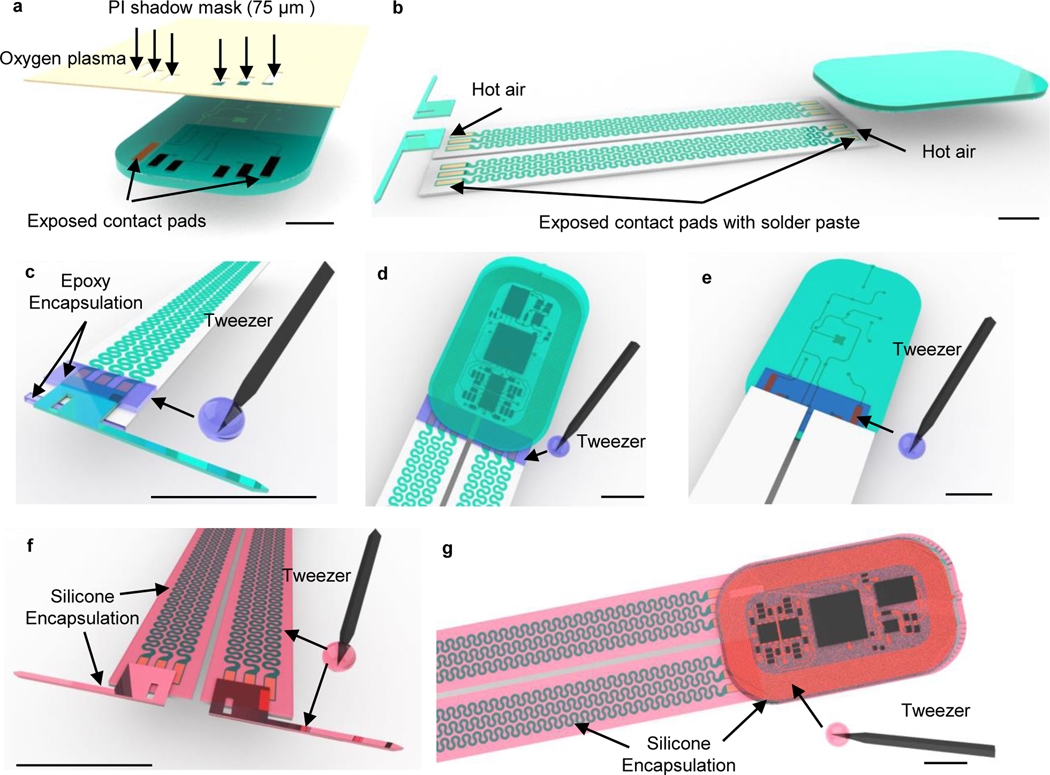
Cut the shadow mask that covers the surface of probes and back side of BM module with contact pads for electric connections exposed on a polyimide sheet (PI, 75 μm) through laser ablation.
Critical Step: The shadow masks should exceed the area of the probes and circuit respectively to protect them from future RIE etching process in step 36.
Pause point: The process can be paused here. Finished PI shadow masks can be stored in plastic containers at room temperature for up to one year.
-
7
Align the shadow mask over the probe and circuit, then seal the edges using PI tape (Fig. 5a and Extended Data Fig. 6a).
Critical step: Accurate alignment between the shadow mask and the device ensures a successful match between the electrical contact pads of the serpentine traces, circuits, and probes in the following soldering process. Edge sealing with PI tape protects the device from unnecessary etching caused by the leak of the gas that downgrades the encapsulation quality.
Pause point: The process can be paused here. Finished devices can be stored in plastic containers at room temperature for up to one year.
-
8
Etch the parylene on top of the exposed contact pads through RIE (For March equipment, use the following settings: gas: O2; Pressure: 220 mTorr; Power: 200 W; Time: ~ 30 min for BM module, ~ 60 min for probes; Fig. 5a).
Critical Step: Similar to step 17, reserve a 5-minute safety time window during the etching process to prevent over etching. Measure the electrical resistance on the etched contact pads with a multimeter to indicate the state of etching. If the multimeter displays an open circuit, the serpentine traces are still not fully etched. Repeat step 36 with 1-minute etching time intervals until the multimeter displays short circuit for all contact pads.
Critical Step: Similar to step 17, precise control over the etching profile, especially in etching time, is important to form successful encapsulation over probes and circuits with contact pads fully exposed for electrical connections.
Pause point: The process can be paused here. Devices can be stored in plastic containers at room temperature for one day at most before the following assembly process.
?Troubleshooting
-
9
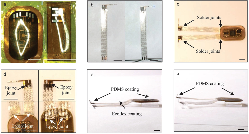
Use a razor blade to cut and detach the soft serpentines from the wafer (after step 26). Solder the probes and circuits on to the prepared soft serpentines with low temperature solder using a hot air gun (Fig. 5b and Extended Data Fig. 6b–6c).
Critical Step: Check the functions in an experimental test set up (starting at step 45) and evaluate electrical connections if malfunction is detected.
Critical Step: Firm electrical bonding between circuit, probes and serpentine traces ensures the devices’ function during deformations induced by animal’s natural movement after implantation.
?Troubleshooting
-
10
Secure and encapsulate the solder joints using 1–2 droplets of dipping epoxy superglue (Fig. 5c–5e, Extended Data Fig. 6d).
Critical Step: This step covers the joints where the parylene encapsulation is etched for electrical connections (step 36) to ensure the full encapsulation of BM device. Incomplete epoxy coverage at joints will cause significant reduction in operation lifetime after implantation.
Pause point: The process can be paused here. Devices can be stored in plastic containers at room temperature for up to one year before the following dip coating process.
-
11
Encapsulate soft serpentines with Ecoflex (~2.5 droplets for each serpentine trace) on their top surfaces. Hang vertically for ~ 2 minutes to remove excessive Ecoflex. Then lay the device flat for ~ 5 minutes to ensure the coating is uniform. Then thermally cure Ecoflex inside a 70 °C convection oven for another 1 hr (Fig. 5f and Extended Data Fig. 6e).
Critical Step: This step covers the top side of the serpentine traces with Ecoflex to protect the serpentine from growing fascia after surgical implantation. Direct contact with fascia will lead to a significant reduction in serpentine stretchability.
-
12
Encapsulate the back surfaces of the probes (the side with the tungsten stiffeners) by dipping PDMS droplets with a tweezer on their surfaces (~ 0.5 droplet for each probe; Fig. 5f and Extended Data Fig. 6e).
-
13
Encapsulate the top surface (the side with the electronic components) of BM module by dripping ~8–10 droplets of PDMS ) on its surface followed by thermal curing of both module and probes (in step 40) inside a 70 °C convection oven for another 1 hr (Fig. 5g and Extended Data Fig. 6e).
-
14
Reverse the device and put it on a flat stage. Encapsulate the front side of the probes (the side with μ-LEDs) with PDMS droplets (~ 0.5 droplet for each) with a tweezer. Then encapsulate the back surface of the module (the side without the electronic components). Thermally cure the PDMS inside a 70 °C convection oven for another 1 hr (Extended Data Fig. 6f).
Critical Step: BM device fabrication is now complete.
Pause point: The process can be paused here. Devices can be stored in plastic containers at room temperature for up to one year before the following implantation process.
Figure 5: Schematics of assembly procedures for back mounted devices.
a, Apply RIE through a polyimide (PI) shadow mask to remove the parylene on contact pads of the back mounted (BM) module. b, Use heat gun, 250 °C and low air speed, to melt indium solder pastes and electrically bond the BM module and injection probes with soft interconnection traces. c-e, Use a tweezer to dip coat epoxy on solder joints at probes (c), top side of the soft interconnections (d), and bottom side of the soft interconnections (e). f, Use a tweezer to dip coat Ecoflex to cover the soft interconnections and PDMS to cover probes. g, Dip coat PDMS on BM electronic module. Scale bars: 5 mm.
Viral transduction
CRITICAL If viral transduction is required for in vivo optogenetic studies, this must be undertaken prior to device implantation. The tools required for viral transduction and subsequent device implantation are summarized in Supplementary Fig. S1. For optimized efficiency and scheduling, we suggest starting virus transduction when device fabrication is expected to finish within a week.
-
6
Transduce virus by following option A for neonates (P1-P6) and option B for weanling and adult animals (>P21). Intracranial injections in neonates are a highly efficient and minimally invasive procedure that uses cryoanesthesia with no incision or sutures due to the direct penetration of skin, skull, and brain by the injection needle. Alternative means of opsin introduction via transgenic crosses or adult viral transduction are available and well-established and can be used in place of this step21,22.
Option A: Virus transduction in the neonatal brain • TIMING 1 d
-
Prepare and sterilize surgical tools and device in accordance with approved animal protocols.
Caution: Prior to completing the following steps, use of the procedure must be approved by the Institutional Animal Care and Use Committee.
-
Attach a pulled glass pipette to the pump head of UltraMicroPump (or other injection system). Load the viral solution into injection pipette.
Critical Step: The length of pulled glass pipette should be adjusted according to the depth of the targeted brain region. The size of the pipette tip used in this protocol ranges from 3 μm to 7 μm.
-
Disinfect gloves with EtOH before touching neonates in the breeding cage. Take out the entire litter of P1–4 neonates and place them into a container warmed by a temperature controller.
Critical Step: All neonates must be removed together using clean gloves to reduce cage disturbance, potential maternal stress, and the risk of cannibalism.
-
Place one neonate at a time on ice for 5 min to induce cryoanesthesia. Protect the neonate from ice surface with aluminum foil (Fig. 6a).
Critical Step: Neonatal skin must stay dry.
Once the animal’s voluntary movement disappears, remove it from the ice chamber and put it onto an ice box. Lightly press the animal’s head with surgical tape to hold the skull in a desired position. Use sterile gloves and sterile technique (Fig. 6b).
Identify the desired coordinates for virus injection using eyes, ears, and cranial suture lines (Fig. 6c).
Penetrate the skin and skull with glass pipette, advance the glass pipette to the desired depth (Fig. 6b).
Deliver AAVs at a rate of 100 – 150 nl/min using an UltraMicroPump controller. After desired amount of AAV is delivered, wait 2–10 min and carefully withdraw the pipette from the brain.
Repeat steps vi-viii, as needed, based on the number of injection sites. Place the neonate on an ACUC-compatible heating blanket protected by a thick tissue. Closely monitor respiratory activity during recovery for 10 – 30 min. Active inspiration and movement indicate appropriate recovery from hypothermia-induced anesthesia. If several pups are used in the procedure, return them together to the breeding cage for minimal disturbance (Fig. 6d).
-
Maintain animals until they are ready for device implantation (>P40).
Critical Step: Adequate viral expression for optogenetic experiments will take approximately 1 to 2 weeks or longer following the injection. During this time the animals will become physically mature.
Figure 6: Viral transduction procedures in neonatal mice.
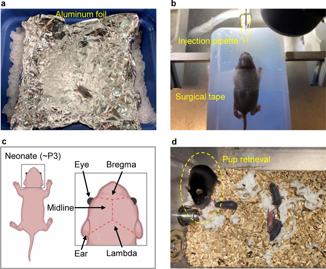
a, Place one neonate on ice, protected by foil, for cryoanesthesia. b, Place the neonate on a dry ice box and secure the body with surgical tape. c, Identify injection coordinates using anatomical markers (eye, ear, bregma, lambda, and midline). d, Warm on a heating pad and return all neonates to the home cage after viral transduction, observe pup retrieval behaviors of the female adult, and monitor the animals according to institutional guidelines.
Option B: Virus transduction in the adult brain • TIMING 1 d
-
Prepare and sterilize injection area, surgical tools, and the device in accordance with your approved animal protocol.
Caution: Prior to completing the following steps, the use of the procedure must be approved by your Institution’s Animal Care and Use Committee.
Anesthetize the animal in an isoflurane induction chamber using 3.0% isoflurane and an oxygen flow rate of 1 L/min.
Attach a pulled glass pipette to the pump head of UltraMicroPump. Load the viral solution into injection pipette.
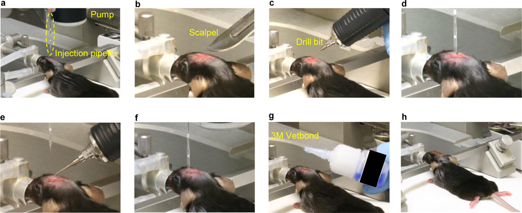
Once the animal is sufficiently anesthetized, remove it from the chamber and shave the top of the head area (Fig. 7a).
-
Place the animal into the nose cone of a stereotaxic frame with 1.5–2.5% isoflurane and a 1 L/min oxygen flow rate (Fig. 7b).
Caution: Monitor the respiratory rate (~1Hz) of the animal throughout the surgical procedure. The isoflurane flow rate should be adjusted throughout the surgery based on respiratory rate.
-
Position the ear bars securely against the skull.
Caution: Proper ear bar positioning is necessary for adequate oxygen flow through the nose cone, as well as preventing movement of the animal’s skull during burr hole drilling and probe placement.
Verify the animal does not respond to a toe pinch, ensuring a sufficient plane of anesthesia, and apply eye lubricant across both eyes to prevent drying during surgery.
Administer pre-operative analgesics and fluids as required by the animal protocol.
Clean the shaved areas by alternating applications of betadine and 70% isopropyl alcohol, three times for each.
Using a scalpel, begin a sagittal midline incision (~1cm) just behind the eye line and continue posteriorly, exposing both bregma and lambda (Fig. 7b).
Using the curved hemostats, clip the edges of the incision to keep the skin from obstructing the view of the cranial suture lines along the skull. Note that this step might not be required if a clear surgical field is present following the previous step.
Clean the skull by removing any fluids or periosteum with a sterile cotton swab.
-
Make adjustments to the angle of the head and ear bars, as needed, until the skull is level in both the anterior-posterior and medial-lateral directions.
Critical Step: Proper stereotaxic placement of the probes within the target brain regions is dependent on the skull being level and is mandatory for experimental success. Anatomical differences in mouse suture lines require the surgeon to develop their own guidelines for identifying bregma and lambda consistently across animals.
Identify the desired coordinates for viral injection.
Use the drill to make burr holes for inserting the glass pipette into the brain (Fig. 7c).
Load the viral solution into injection pipette. Direct the pipette to bregma and mark the coordinates. Then navigate the glass injection pipette to the desired coordinates (Fig. 7d).
Deliver AAVs through a pulled glass pipette at a rate of 100 nl/min using an UltraMicroPump. After desired amount of AAV is delivered, wait 3–5 min for AAVs to diffuse into the target brain region, then carefully withdraw the pipette 300 μm and wait an additional 3 minutes before fully retracting the glass pipette from the brain (Fig.7d)
Repeat steps xiv-xvii, as needed, based on the number of injection sites (Fig. 7e–7f).
Close the incision with sutures or Vetbond, and administer analgesics and hydration fluids in accordance with your animal protocol’s post-operative care requirements (Fig. 7g–7h).
Maintain animals until they are ready for device implanation. Note that adequate viral expression in the targeted brain regions will take approximately 2–4 weeks following the injection.
Figure 7: Viral transduction procedures in adult mice.
a, Load the virus solution into an injection pipette, prepare the surgical space. b, Make an incision using scalpel. c, Confirm the implantation coordinates and drill insertion holes. d, Proceed the injection pipette to the desired coordinates and deliver the virus solution. e-f, Repeat the procedures in c-d if needed. g, Close the wound with Vetbond or alternatives. h, Monitor the animal according to institutional guidelines.
Device implantation
CRITICAL Devices must be implanted at least two weeks after any viral transduction.
-
6
Follow option A to implant HM devices and option B to implant BM devices.
Option A: HM device implantation (applies to both active and passive devices) • TIMING 0.5 d
CRITICAL Implantation procedures for active and passive HM devices are similar and included in Fig. 8 and Extended Data Fig. 7, respectively.
Figure 8: Implantation procedures for active head mounted devices.
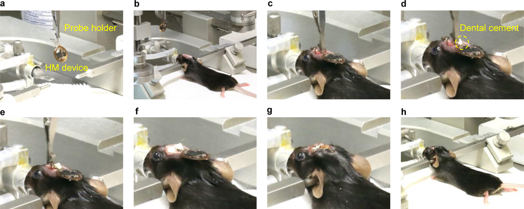
a, Clamp the first probe with a probe holder that mounts on a stereotaxic arm. b, Prepare the surgical space, make an incision, confirm the implantation coordinates and drill insertion holes. c, Insert the first probe. d, Use dental cement to fix the injected probe. e, Insert the second probe. f, fix the position of the second probe and withdraw the probe holder. g, Position the device coil and cover it with the surrounding skin. h, Suture the skin and proceed with post-operative steps and monitoring according to institutional guidelines.
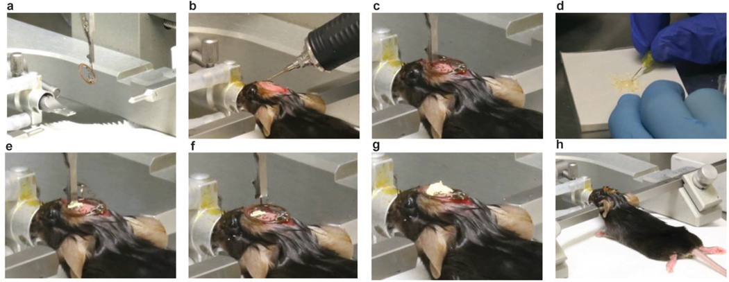
Undertake steps i-xv in “Virus transduction Option B” to anesthetize the animal, position it in a stereotaxic frame, and drill burr holes in the skull for virus injection. The μ-ILEDs direct light laterally, so, if required, drill additional holes 200–300 μm adjacent to the injection site for probe placement (Fig. 8a–8b).
Attach probe holder to the stereotaxic arm.
-
Using the curved forceps, slightly extend both serpentines and place the flag of one probe into the probe clip and secure onto the arm (Fig. 8a), lower the probe carefully and place the coil onto animal’s neck.
Critical Step: Verify that the flag is aligned vertically and the μ-ILED is facing towards the brain region of interest. The tungsten backer will be on the opposite side of the probe from the μ-LED. The probe tip needs to be lowered 420 μm lower than the virus injection site to adjust for the μ-LED position on the probe.
Direct the probe to bregma and mark the coordinates. Then proceed to navigate the probe to the desired coordinates (Fig. 8c).
-
Using a small gauge needle (between 25–31 gauge), apply a small drop of dental cement around the junction of the probe and skull. Use a disposable brush to apply a small drop of the adhesive activator to quickly harden the glue and secure the probe in place (Fig. 8d).
Critical Step: Depending on the size of the gap between the skull and the flag, the glue can easily glide upwards towards the clip, leading to the clip being permanently adhered to the probe. It is imperative that the super glue be applied in sequential steps, with a droplet of glue no larger than the bevel of the syringe needle during each application. There need only be a sufficient amount of glue to ensure the probe will not be jostled upon removing the clip.
Carefully release the alligator clip from the probe flag, using a pair of curved forceps to assist as needed, and retract the stereotaxic arm.
Remove the clip from the probe holder and place the flag of the next probe in the clip (Fig. 8e).
Again, direct the probe to bregma and mark the coordinates. Guide the probe to the desired coordinates and secure in place using super glue as described in step iv-v (Fig. 8e).
Remove the clip from the second probe.
Once the probes are secured within the skull, use forceps to fold the flags inwards toward the midline of the skull so the serpentines lay flat.
-
Secure the flags to the skull by placing a drop of super glue on the skull, then apply downward pressure onto the flags using the curved forceps. Apply a small drop of adhesive activator using a disposable brush (Fig. 8f).
Critical Step: Be careful not to super glue the forceps to the flags while applying pressure. Steps x-xi are optional if the height of flags does not exceed the level of surrounding tissue.
Apply a small amount of MMA or dental cement around the anterior edges of the flags. Make sure there are no sharp or rough edges that can rub against the skin once the incision is closed (Fig.8f).
Carefully lower the coil onto the skull and use forceps to cover the coil with the skin around the incision (Fig. 8g).
Close the incision with sutures and administer analgesics and hydration fluids in accordance with your animal protocol post-operative care (Fig.8h).
Remove the animal from the stereotaxic frame and place in a heated recovery chamber.
Once the animal is alert and responsive, place in a clean home cage and return to vivarium for recovery. Allow animals to recover for at least 3–7 days before proceeding to any behavioral experiments.
Option B: BM device implantation TIMING 0.5 d
-
Undertake steps i-xv in “Virus transduction Option B” to anesthetize the animal, position it in a stereotaxic frame, and drill burr holes in skull for virus and probe placement (Fig. 9a–9e).
Critical Step: In addition to shaving the head, also shave the lumbar region of the animal’s back.
Using a small pair of scissors, create a ~1 cm long incision in the skin across the back, perpendicular to the spine and just below the thoracic vertebrae (identified by the natural hump of the spine when the animal is prone; Fig. 9f).
Use a small pair of curved hemostats to create a subcutaneous pocket in the fascia along the spine for the device to traverse. Insert the closed hemostats into the incision at the base of the skull, with the curve of the mouth pointing upwards (Fig. 9g).
Using blunt forceps, hold the skin of the back taut and slide the hemostats ~1 cm under the skin. Ensure that the tips of the curved hemostats are pressed against the skin and not downward towards the back musculature (Fig. 9h).
Open the hemostats ½ inch and retract the open hemostats anteriorly towards the head incision to gently tease apart the connecting fascia (Fig. 9h).
-
Close the hemostats outside the animal and reinsert under the skin, advancing the hemostats posteriorly ~1 cm at a time. After each advance, open the hemostats ½ inch and retract anteriorly. Repeat these steps until the tip of the hemostats reaches the back incision (Fig. 9i).
Critical Step: The pocket needs to be large enough to accommodate implanting the device, but not so large that the device can slide side to side laterally underneath the animal’s skin before healing in place.
Caution: There should be no resistance against the hemostats. If resistance is felt, the hemostats may be pressing against muscle or you may be advancing the hemostats too aggressively.
Using blunt forceps, place the back edge of the device into the incision at the base of the skull. Verify the orientation of the device so that the serpentine coils are lying flat and the probes are not in danger of being bent (Fig. 9j).
-
Insert the blunt forceps into the back incision and navigate them through the pocket created with the hemostats (steps iii-vi). Grab the posterior edge of the device and pull posteriorly through the pocket until the back of the device meets the incision point (Fig. 9k).
Critical Step: Pay close attention to the position of the probes and serpentine coils while pulling the device through the pocket. The serpentines should lay flat under the skin with no bulging.
?Troubleshoot
-
Repeat steps ii-xvi in “Device implantation Option A” to implant probes, suture incisions and prepare the animal for recovery. (Fig. 9l – 9t). Allow the animals to recover for at least 3–7 days before proceeding to any behavioral experiments.
Pause point:
Figure 9: Implantation procedures for back mounted devices in mice.
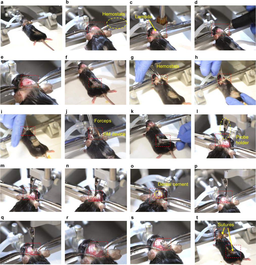
a, Prepare the surgical space on the skull and the back region of the animal. b, Make an incision on the scalp, hold the edges of skin using hemostats. c, Identify bregma and lambda and level the skull. d-e, Confirm the implantation coordinates and drill injection holes. f, Make an incision on the back skin. g-i, Use hemostats to create a subdermal space to implant the device coil. j-k, Use forceps to position the device coil subdermally on the back region. l-n. Inject the first probe. o, Secure the first probe with dental cement. p-q, Insert the second probe. i, Secure the second probe with dental cement. s-t, Suture the skin and proceed with post-operative steps and monitoring according to institutional guidelines.
Setup of equipment for optogenetic studies TIMING 0.5 d
CRITICAL The system requires a power distribution box, antenna tuner box, and laptop with compatible software. In this procedure, we describe the use of products from Neurolux Inc. Research groups that cannot obtain Neurolux products, should refer to our previous publication for instructions for setting up a generic wireless RF power transfer system with off the shelf commercial hardware1.
-
6
Take a 16–22 gauge wire, starting 3 cm from the base and at the center of one side of the experimental enclosure, and do one full turn around the cage keeping the wire at the same height. Then, without cutting the wire, start a new full turn around the cage 9 cm above the base. This procedure forms a double loop RF primary antenna that enables wireless power transfer and NFC communication to the wireless devices (Extended Data Fig. 8).
Critical step: The rotation of the double loop antenna should follow the same direction to ensure a strong and stable magnetic field. We suggest using a 30 cm × 30 cm experimental enclosure with double loop primary antenna at heights of 3 cm and 9 cm from the base. Yang et al. have provided a complete database on optical intensity, temperature increment, light penetration depth, and effective stimulation volume with respect to primary antenna power, stimulation frequency and duty cycle, and implantation depths for both HM and BM devices over this particular primary antenna configuration14. Any changes in device geometry and circuitry, as well as primary antenna configuration, require recalibration of electrical and optical power to obtain accurate illumination profile. The calibration process is explained in the previous publication14.
Critical Step: The primary antenna configuration determines the inductive power received by the wireless device, thus determining illumination profile.
-
7
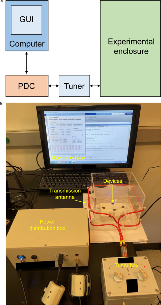
Connect the primary antenna, tuner box, power distribution box (PDB), and laptop. Power up the system and set an output power of 2 W. Then, tune the resonance frequency to 13.56 MHz using the tuner box (Extended Data Fig. 8). Once it is tuned, increase the output power to the desired operational power and tune again. Repeat this step before every behavioral experiment to ensure optimal coupling between the primary antenna and wireless device. The tuner box modifies the capacitance of the primary antenna to shift its resonant frequency to the operating RF and to adjust its load. The two knobs on the tuner box provide frequency and load tuning. The knob labeled “tune” shifts the resonance frequency, while the knob labeled “load” modifies the load on the antenna, which in turn maximizes the power transfer from the RF driver to the antenna. Antenna tuning is performed sequentially: first turn the “tune” knob until its indicator turns blue then slowly rotate the knob “load” until both indicators turn blue.
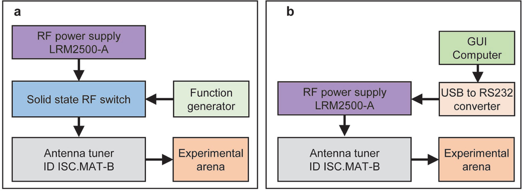
Critical Step: Instructions for users that cannot use Neurolux products are available in our previous publication 1,10, see also Extended Data Fig. 9. In brief, for operating passive devices, the RF power transfer system employs an RF power supply (LRM2500-A, Feig Electronics), square wave signal generator, generic solid state RF switch, and antenna tuning board (ID ISC.MAT-B, Feig Electronics) that operates in the 13.56 MHz RF band. Connect the RF power supply output to the input of the RF switch using an SMA coaxial cable. Connect the output of the signal generator to the RF switch control input. Finally, connect the output of the RF switch and transmission antenna with the antenna tuning board using SMA coaxial cables (Extended Data Fig. 9a). For operating active smart NFC devices, the RF power transfer system uses an RF power supply (LRM2500-A, Feig Electronics), a computer that runs the GUI supplied in this protocol, a generic USB to RS232 converter cable, and an antenna tuning board (ID ISC.MAT-B, Feig Electronics) that operates in the 13.56 MHz RF band. Connect the computer to the RF power supply RS232 input via the USB to RS232 converter to establish communication with the RF power supply. Then, connect the output of the power supply and the transmission antenna with the impedance matching board (Extended Data Fig. 9b). In both configuration the antenna must be properly tuned. With the use of a network analyzer (RIGEXPERT AA-54, Rig Expert Ukraine, Ltd.), tune the antenna using the impedance matching board to 13.56 MHz and 50 ohm impedance for optimal energy transfer.
Critical Step: Frequency mismatch will significantly reduce the inductive power received by the device, leading to inaccurate quantification of illumination profiles during experiments.
-
8
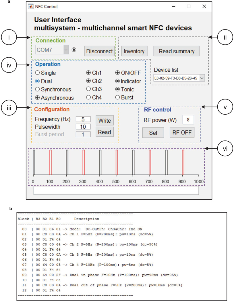
Open the graphic user interface (GUI) file (SmartDevices.m; available at ref18) in MATLAB script editor and hit the run command to open the interactive GUI. Hit the “Connect” button to establish communication with the PDB box (Extended Data Fig. 10a–i). Place the animals implanted with either HM of BM devices inside the experimental enclosure and hit the “Inventory” button to collect the ID of each animal in the cage (Extended Data Fig. 10a–ii). The drop-down menu “Device list” will contain the list of devices found in the cage, which can be individually addressed. The power delivered by the PDB can be adjusted using the power setting (in the range of 2–12 W). In addition, the RF field can be activated/deactivated by pressing the “RF ON/OFF” button (Extended Data Fig. 10a–v).
Critical Step: The GUI runs in both Mac and Windows operating systems (OS) running MATLAB 2017a or newer versions. The communication port label varies across operating systems; in Mac it reads as “tty.[…]” where “[…]” indicates the label assigned by the OS; in Windows it reads as “COMX” where “X” indicates the number assigned by the OS. If the port is not selected properly there will be a message in the command windows stating “Wrong port”.
Critical Step: Make sure the appropriate drivers are installed in the computer to ensure proper OS communication with the system.
-
9
Each mode of operation has its own set of configurations in the device. In order to update these parameters, set the frequency (in Hz) and then introduce pulse width (in milliseconds) and hit the “Write” button. This will load the timing configuration parameters to the selected device. To read the current values stored in memory, select the channel and mode and hit the “Read” button. The current values will show in the “Frequency” and “Pulse width” boxes (Extended Data Fig. 10a–iii). The command button “Read summary” generates a report of all the parameters in the memory (Extended Data Fig. 10a–ii and Extended Data Fig. 10b). The bottom panel in the GUI (Extended Data Fig. 10a–vi) shows a representation of the waveform generated with the parameters set.
Critical Step: The timing parameters are stored in memory. It is unnecessary to resend the parameters when undertaking subsequent experiments using the same values.
-
10
Once the devices are recognized by the GUI, several modality commands can be issued using the “Operation” section. For example, for single channel operation select the option “Single”, then select which channel “Ch1 – 4” to operate (Extended Data Fig. 10a–iv). For dual channel mode of operation, select the option “Dual”, then select two arbitrary channels “Ch1–4”. Dual channel operation modality has two selectable operation modes “Synchronous” and “Asynchronous”, which corresponds to in-phase illumination and out-of-phase illumination, respectively. The channel selection and modality take effect immediately. In addition, the options “ON/OFF” and “Indicator” turns on/off whichever modality the device is operating and the indicator on the device, respectively. Pressing the “ON/OFF” option again resumes previous modality. During “Burst” modality the bursting period is specified in the corresponding input box in the configuration panel (Extended Data Fig. 10a–iii).
Anticipated results
This protocol offers detailed procedures for fabrication and implantation of new generation wireless optogenetic devices and proposed experimental systems the neuroscience community can employ. A successfully fabricated device should have the following features: 1) wireless battery-free operation; 2) long-term stability after implantation; 3) real-time programmable capabilities if necessary (active devices). In addition, the implantable wireless probes should induce similar immune-responses and gliosis to those resulting from the use of conventional fiber optics14. The implanted wireless devices are expected to minimize the interference with naturalistic behavior (e.g., locomotion, climbing, social interactions, etc.). With integrated NFC and microcontroller operation, scientists can design individualized optical stimulation parameters for different subjects within the same experimental arena14. Animals expressing an opsin may display certain behavioral changes upon optogenetic activation/inhibition of the targeted neuronal groups23. Conversely, animals without opsin expression should not show any behavioral changes. Researchers should avoid potential thermal effects induced by optical simulation at high duty cycles that may interfere with some behavioral readouts19. It is important appropriate controls are implemented for all behavioral assays.
Further integration of additional electronic systems into current design, for example capacitor banks, may enable additional power regulation capacities to be achieved and permit transcranial stimulation at higher light intensities23. Other extensions of the current platform include sensing modalities such as photometric recording of genetically encoded sensors, electroencephalogram, electrochemical sensing, or reservoirs and microfluidic channels that enable liquid drug delivery for multimodal photopharmacology neuromodulations.
Troubleshooting
Troubleshooting guidance can be found in Table 1.
Table 1:
Troubleshooting Table
| Step | Problem | Possible reason | Possible solution |
|---|---|---|---|
| 3 | Electrical disconnections at vias or electrical shortage between adjacent traces. | Filling process of silver paint is not done carefully, or the silver paint is too viscous. | For electrical disconnection at via holes, puncture out the silver paint with a sharp needle and refill with fresh silver paint. For electrical shortage between adjacent traces, clean the spread silver paint with a sharp needle or razor blade. |
| 4 | Shift or loss of resonance frequency. | Wrong capacitance or improper circuit connections. | For shifted resonance frequency, adjust the capacitance accordingly. For loss of resonance frequency, repeat troubleshooting process in step 3 to fix circuit connections. |
| 6 | Failed blinking of indicator or stimulator μ-ILEDs. | Bad soldering between electronic components (NFC, microcontroller, and μ-ILEDs) and circuit traces. | For failed blinking of indicator μ-ILED, re-solder NFC and microcontroller to make sure their electrical connection integrities. For failed blinking of stimulator μ-ILEDs, inspect the electrical connection from the microcontroller to the μ-ILED. |
| 8 | Failed download of firmware to the microcontroller. | Bad electronic connection integrity between microcontroller and IC socket. | Confirm the mounting of microcontroller inside IC socket. Make sure the pins are correct and the electrical connections are good. |
| 13 | Wrong resistance values of serpentine traces, including the breakage of traces and shortage between adjacent traces. | Under or over development of exposed photoresist, as well as under or over etching of metal layers. | Disregard failed serpentine traces on the wafer if the majority of them remain good. If the majority of the traces failed, remove all photoresist with acetone and metal layers with corresponding etchants, and restart the process from step 12. |
| 17 | Serpentine traces fail to show resistances when measured at the contact pads. | Insufficient RIE etching. | Repeat step 17 every 5 minutes until the contact pads of serpentine traces show resistance when measured. |
| 36 | Contact pads on BM module fail to show resistances when measured. | Insufficient RIE etching. | Repeat step 36 every 5 minutes until the contact pads of BM module show resistance when measured. |
| 37 | Malfunction of the BM devices. | Bad soldering between serpentine traces and probes or modules | Re-solder electrical connections. |
|
Device implantation
Option B Step viii |
The edges of the device tug on the fascia. | The pocket is not wide enough. | Remove the device and further tease apart the fascia with the hemostats. |
Extended Data
Extended Data Figure 1: Preparation of the electronic module and probes.
a, Apply laser ablation to form the geometrical layouts and circuit footprints for electronic modules and probes. b, Use ultrasonic flux bath to clean the surfaces of modules and probes after laser ablation. c-e, Fill in laser-ablated via holes with liquid silver paint using a 30 gauge blunt needle to make electrical connections between top and bottom circuits. (c) Active HM device. (d) BM module. (e) Passive HM device. (f) probes for BM devices. g-j, Solder electronic components on circuit footprint. (g) Active HM device. (h) BM module. (i) Passive HM device. (j) probes for BM devices. k-m, Device operation. (k) Passive HM device. (l) Active HM device. (m) BM module.
Extended Data Figure 2: Attiny84 microcontroller programming using Arduino IDE.
The microcontroller is programmed using open-source Arduino software, commercial ISP programmer and QFN20 packaging adapter socket. (i) Open the microcontroller firmware using Arduino. Set the corresponding programming parameters. (ii) Connect the programmer to the computer. (iii) Mount the microcontroller chip onto the QFN20 socket and secure properly. Upload the firmware to the microcontroller.
Extended Data Figure 3: Preparation of soft interconnections for back mounted devices.
a, Apply photolithographic method to define the serpentine geometries for metallic and SiO2 layers. b, Use RIE to define the serpentine geometries of parylene encapsulation layers. The contact pads are exposed for electrical connections. c-f, Transfer printing process. (c) Cover the silicon wafer with a thin wipe (Kimtech) and another same sized silicon wafer and put it in an 80 °C acetone bath for 90 minutes. (d) Use water soluble tape to transfer the interconnection traces from silicon substrate. (e) Bond the interconnection traces on silicone substrate. (f) Dissolve tape in distilled water.
Extended Data Figure 4: Preparation of tungsten strengthened probes.
Glue tungsten stiffeners on (a) the active HM device, (b) the passive HM device, and (c) the probe for BM device. Scale bars: 5 mm.
Extended Data Figure 5: PDMS coatings for head mounted devices.
a, Use a sharp tweezer to dip PDMS droplets to cover the coils, electronic components, serpentine connections, and probes of an active HM device laying on a flat stage. b, Same dip coating process applied at top side of a passive HM device. c, Same dip coating process applied at back side of an active HM device. d, Same dip coating process applied at back side of a passive HM device. Scale bars: 5 mm.
Extended Data Figure 6: Assembly of back mounted devices.
a, Cover the BM module and probe with PI shadow mask with contact pads exposed. RIE process removes the parylene coatings on contact pads, allowing future electrical connections among these components. b, Solder the probe on soft interconnection traces (left). Verify the electrical connections by powering the μ-ILED with multimeter (right). c, Solder the soft interconnection traces on the BM module to complete the assembly. d, Encapsulate the solder joints with epoxy. The joints include the back side of the probe’s flag (top left), top side of the ends of soft serpentine traces (bottom left), top side of the probe’s flag (top right), and back side of the ends of soft serpentine traces (bottom right). e, Use a sharp tweezer to dip Ecoflex droplets on the top side of serpentine traces followed by thermal curing. Then dip PDMS droplets on top side of the BM module and back side of probes (the side with the tungsten stiffeners) followed by thermal curing. f, Similar dip coating process with PDMS droplets is applied at the back side of the BM device including the back side of the electronic module and the front side of the probes (with μ-ILEDs). Scale bars: 5 mm.
Extended Data Figure 7: Implantation procedures for passive head mounted devices.
a, Clamp the first probe. b, Prepare the surgical space, make an incision, confirm the implantation coordinates and drill insertion holes. c, Insert the first probe. d-e, Use dental cement to fix the injected probe. f, Insert the second probe. g, fix the position of the second probe and withdraw the probe holder. h, Suture the skin and proceed with post-operative steps and monitoring according to institutional guidelines.
Extended Data Figure 8: Experimental implementation.
a, Block diagram that indicates the implementation of the typical wireless optogenetics system. The graphic user interface (GUI) is hosted on a computer and interfaces with the power distribution controller (PDB) via serial interface. The PDB box drives radio frequency power at 13.56 MHz to the transmitting antenna on the experimental enclosure and transfers wireless power to the receiving antennae on the NFC devices. The impedance of the transmission antenna is properly matched using an impedance tuner (Tuner). The PDB, besides providing RF power, also relays read/write commands instructed from the GUI to the NFC device as the basis of wireless control of the mode of operation of the implantable devices. b, Photograph of a typical experimental implementation showing the hardware described in (a).
Extended Data Figure 9: Implementation of a generic wireless power transfer system for passive and active devices.
a, Block diagram that shows the implementation of the RF system for operating passive devices. b, Block diagram that shows the implementation of a system for operating smart NFC devices.
Extended Data Figure 10: Graphic user interface.
a, Screenshot of the GUI designed to control multiple devices sharing the same experimental arena. The GUI connects to the PDB box using commands in block (i). Commands in block (ii) allow the detection of devices in the RF field (Inventory) which are then listed in dropdown menu (Device list). The command “Read summary” interrogates the selected devices and provides a summary of the parameters currently stored in the device’s memory (see b). Commands in block (iii) read (Read) and write (Write) parameters such as Frequency, Pulse width and Burst period to the selected device and selected mode of operation. Commands in block (iv) provide access to the mode of operation of the devices. Options such as Single or Dual mode of operation, as well as the channel selection or tonic or burst stimulation modes, is specified here. Commands in block (v) provides access to the RF parameters of the PDB box, such as power setting or toggling the operation status of the RF field, i.e. ON/OFF operation. Finally, block (vi) shows a snapshot of the waveform that the device will produce based on the parameters specified in blocks iii and iv. b, Screenshot of the configuration summary currently stored in the memory of the device produced when hitting the “Read summary” command button in block ii. If the experiment does not require further adjustment of these parameters, only commands such as those specified in block (iv) will need subsequent changes.
Supplementary Material
Supplementary Figure 1: Tools for virus transduction and device implantation.
Acknowledgement
This work utilized Northwestern University Micro/Nano Fabrication Facility (NUFAB), which is partially supported by Soft and Hybrid Nanotechnology Experimental (SHyNE) Resource (NSF ECCS-1542205), the Materials Research Science and Engineering Center (DMR-1720139), the State of Illinois, and Northwestern University. C.H.G is supported by the LUCI program, sponsored by the Basic Research Office, Office of Under Secretary of Defense for Research and Engineering (USD R&E). Y.K. is supported by the NIH R01MH117111 and R01NS107539, and Beckman Young Investigator Award. M.W is supported as an affiliate fellow of the NIH T32 AG20506 and 2021 Christina Enroth-Cugell and David Cugell Fellow. Z.X. acknowledges the support from the National Natural Science Foundation of China (Grant No. 12072057), LiaoNing Revitalization Talents Program (Grant No. XLYC2007196) and Fundamental Research Funds for the Central Universities (Grant No. DUT20RC(3)032). Y.H. acknowledges support from NSF (CMMI1635443).
Footnotes
Tweet
Preparation and use of real-time wireless reprogrammable multilateral optogenetic devices for rodent behavioural studies
Cover teaser
Wireless smart optogenetic devices
Code availability
The computer code for customized graphical user interface is available at https://doi.org/10.5281/zenodo.559287318.
Conflict of interest
J.A.R. and A.B. are cofounders in a company, Neurolux, Inc., that offers related technology products to the neuroscience community.
Data availability
There are no new data included in this manuscript. The circuit and serpentine design files are available at https://doi.org/10.5281/zenodo.559287318.
References
- 1.Shin G. et al. Flexible Near-Field Wireless Optoelectronics as Subdermal Implants for Broad Applications in Optogenetics. Neuron 93, 509–521.e3 (2017). [DOI] [PMC free article] [PubMed] [Google Scholar]
- 2.Park S. Il et al. Soft, stretchable, fully implantable miniaturized optoelectronic systems for wireless optogenetics. Nat. Biotechnol 33, 1280–1286 (2015). [DOI] [PMC free article] [PubMed] [Google Scholar]
- 3.McCall JG et al. Fabrication and application of flexible, multimodal light-emitting devices for wireless optogenetics. Nat. Protoc 8, 2413–2428 (2013). [DOI] [PMC free article] [PubMed] [Google Scholar]
- 4.Montgomery KL et al. Wirelessly powered, fully internal optogenetics for brain, spinal and peripheral circuits in mice. Nat. Methods 12, 969–974 (2015). [DOI] [PMC free article] [PubMed] [Google Scholar]
- 5.Kim T. -i. et al. Injectable, Cellular-Scale Optoelectronics with Applications for Wireless Optogenetics. Science (80-. ). 340, 211–216 (2013). [DOI] [PMC free article] [PubMed] [Google Scholar]
- 6.Pisanello F. et al. Multipoint-emitting optical fibers for spatially addressable in vivo optogenetics. Neuron 82, 1245–1254 (2014). [DOI] [PMC free article] [PubMed] [Google Scholar]
- 7.Wu F. et al. Monolithically Integrated μLEDs on Silicon Neural Probes for High-Resolution Optogenetic Studies in Behaving Animals. Neuron 88, 1136–1148 (2015). [DOI] [PMC free article] [PubMed] [Google Scholar]
- 8.Mickle AD et al. A wireless closed-loop system for optogenetic peripheral neuromodulation. Nature 565, 361–365 (2019). [DOI] [PMC free article] [PubMed] [Google Scholar]
- 9.Hibberd TJ et al. Optogenetic Induction of Colonic Motility in Mice. Gastroenterology 155, 514–528.e6 (2018). [DOI] [PMC free article] [PubMed] [Google Scholar]
- 10.Gutruf P. et al. Fully implantable optoelectronic systems for battery-free, multimodal operation in neuroscience research. Nat. Electron 1, 652–660 (2018). [Google Scholar]
- 11.Gutruf P. & Rogers JA Implantable, wireless device platforms for neuroscience research. Curr. Opin. Neurobiol 50, 42–49 (2017). [DOI] [PubMed] [Google Scholar]
- 12.McCall JG et al. Preparation and implementation of optofluidic neural probes for in vivo wireless pharmacology and optogenetics. Nat. Protoc 12, 219–237 (2017). [DOI] [PubMed] [Google Scholar]
- 13.Burton A. et al. Wireless, battery-free subdermally implantable photometry systems for chronic recording of neural dynamics. Proc. Natl. Acad. Sci. U. S. A 117, 2835–2845 (2020). [DOI] [PMC free article] [PubMed] [Google Scholar]
- 14.Yang Y. et al. Wireless multilateral devices for optogenetic studies of individual and social behaviors. Nat. Neurosci 24, 1035–1045 (2021). [DOI] [PMC free article] [PubMed] [Google Scholar]
- 15.Kale RP, Kouzani AZ, Walder K, Berk M. & Tye SJ Evolution of optogenetic microdevices. Neurophotonics 2, 031206 (2015). [DOI] [PMC free article] [PubMed] [Google Scholar]
- 16.Sidor MM et al. In vivo Optogenetic Stimulation of the Rodent Central Nervous System. J. Vis. Exp 1–12 (2015) doi: 10.3791/51483. [DOI] [PMC free article] [PubMed] [Google Scholar]
- 17.Etter G. et al. Optogenetic gamma stimulation rescues memory impairments in an Alzheimer’s disease mouse model. Nat. Commun 10, 1–11 (2019). [DOI] [PMC free article] [PubMed] [Google Scholar]
- 18.Yang Y. et al. Preparation and Use of Wireless Reprogrammable Multilateral Optogenetic Devices for Behavioral Neuroscience. Smart NFC Optogenetics 10.5281/zenodo.5592873 (2021). [DOI] [PMC free article] [PubMed] [Google Scholar]
- 19.Owen SF, Liu MH & Kreitzer AC Thermal constraints on in vivo optogenetic manipulations. Nat. Neurosci 22, 1061–1065 (2019). [DOI] [PMC free article] [PubMed] [Google Scholar]
- 20.Zhang F. et al. The microbial opsin family of optogenetic tools. Cell 147, 1446–1457 (2011). [DOI] [PMC free article] [PubMed] [Google Scholar]
- 21.Wu M. et al. Attenuated dopamine signaling after aversive learning is restored by ketamine to rescue escape actions. Elife 10, 1–30 (2021). [DOI] [PMC free article] [PubMed] [Google Scholar]
- 22.Wu M, Minkowicz S, Dumrongprechachan V, Hamilton P. & Kozorovitskiy Y. Ketamine rapidly enhances glutamate-evoked dendritic spinogenesis in medial prefrontal cortex through dopaminergic mechanisms. Biol. Psychiatry 89, 1096–1105 (2021). [DOI] [PMC free article] [PubMed] [Google Scholar]
- 23.Ausra J. et al. Wireless, battery-free, subdermally implantable platforms for transcranial and long-range optogenetics in freely moving animals. Proc. Natl. Acad. Sci 118, 1–12 (2021). [DOI] [PMC free article] [PubMed] [Google Scholar]
Associated Data
This section collects any data citations, data availability statements, or supplementary materials included in this article.
Supplementary Materials
Supplementary Figure 1: Tools for virus transduction and device implantation.
Data Availability Statement
There are no new data included in this manuscript. The circuit and serpentine design files are available at https://doi.org/10.5281/zenodo.559287318.


