

Abstract
The process of deep texturization of the crystalline silicon surface is intimately related to its promising diverse applications, such as bactericidal surfaces for integrated lab-on-chip devices and absorptive optical layers (black silicon—BSi). Surface structuring by a maskless texturization appeals as a cost-effective approach, which is up-scalable for large-area production. In the case of silicon, it occurs by means of reactive plasma processes (RIE—reactive-ion etching) using fluorocarbon CF4 and H2 as reaction gases, leading to self-assembled cylindrical and pyramidal nanopillars. The mechanism of silicon erosion has been widely studied and described as it is for the masked RIE process. However, the onset of the erosion and the reaction kinetics leading to defined maskless patterning have not been unraveled to date. In this work, we specifically tackle this issue by analyzing the results of three different RIE recipes, specifically designed for the purpose. The mechanism of surface self-nanopatterning is revealed by deeply investigating the physical chemistry of the etching process at the nanoscale and the evolution of surface morphology. We monitored the progress in surface patterning and the composition of the etching plasma at different times during the RIE process. We confirm that nanopattering issues from a net erosion, as contributed by chemical etching, physical sputtering, and by the synergistic plasma effect. We propose a qualitative model to explain the onset, the evolution, and the stopping of the process. As the RIE process is started, a high density of surface defects is initially created at the free silicon surface by energetic ion sputtering. Contextually, a polymeric overlayer is synthesized on the Si surface, as thick as 5 nm on average, and self-aggregates into nanoclusters. The latter phenomenon can be explained by considering that the initial creation of surface defects increases the activation energy for surface diffusion of deposited CF and CF2 species and prevents them from aggregating into a continuous Volmer–Weber polymeric film. The clusterization of the polymer provides the self-masking effect since the beginning, which eventually triggers surface patterning. Once started, the maskless texturing proceeds in analogy with the masked case, that is, by combined chemical etching and ion sputtering, and ceases because of the loss of ion energy. In the case of CF4/H2 RIE processes at 10% of H2 and by supplying 200 W of RF power for 20 min, nanopillars of 200 nm in height and 100 nm in width were formed. We therefore propose that a precise assessment of surface defect formation and density in dependence on the initial RIE process parameters can be the key to open a full control of outcomes of maskless patterning.
1. Introduction
The concept of black silicon (BSi) refers to the silicon surface being patterned into high-aspect ratio nanopillars, conferring excellent optical absorption and antireflection properties (black appearance) due to efficient light trapping.1−3 This quality may strongly contribute to the overall efficiency of Si-based optoelectronic detectors and photovoltaic cells.4−6 In totally diverse application fields, the BSi morphology results in antibacterial properties that make it appealing also for biological and medical applications.7,8 Surface nanopatterning of silicon can be obtained with the aid of several techniques, namely, laser ablation,9 metal-assisted chemical etching,10 electrochemical wet etching,11 and—last but not least—dry plasma reactive-ion etching (RIE).12−14 Fabrication by wet chemical etching is simple and economical, but the increasing costs of waste treatment disposal and environmental concerns made it less attractive over recent years. Furthermore, since wet etchants are active preferentially along a specific crystal orientation,15 they are not adequate to pattern the surface of multicrystalline silicon (mc-Si), as it is typically the case, for example, for photovoltaic mc-Si solar cells. Such a limitation can be overcome by surface laser ablation via laser scanning, which however is a rather slow technique and not very well suitable for large-scale production. Besides, laser patterning can lead to material damage and defects that can affect electronic transport properties.16 In this context, maskless dry RIE has emerged as a sustainable and cost-effective method to fabricate BSi on a wafer scale. Typically, a fluorine-based RIE process is used, which employs SF6 and O2 gases to generate fluoride and oxygen radicals (F* and O*) in the plasma phase, with a mean lifetime longer than the bed residence time so that ions reach the substrate while still being reactive. Successful ultrablack silicon has been already obtained in a maskless RIE process by using SF6 and O2 gases.17,18 As F* radicals react with Si, the volatile compound SiF4 is formed and removed, resulting in surface etching. At the same time, aggregates of the SiOxFy polymeric film are also formed and randomly deposited over the surface. The polymeric film acts as a thin protection layer from etching, thereby generating an automasking effect. However, the passivation layer is then partly removed and perforated by the simultaneous, biased ion bombardment. The trade-off between the formation of the passivation layer and its removal typically limits its thickness to around 2.5 nm, a value at which the chemical etching of the Si surface with F* can still proceed.19 The competition between deposition of the passivation layer and its removal by energetic ion bombardment also causes local variations in the etching rate of the Si surface ending in random nanostructuring. The BSi morphology can be adjusted by changing the RIE parameters, such as gas mixture composition, flow rates, temperature, reaction time, substrate bias, and RF power.20 Different fluorine-based RIE processes are also successful in obtaining BSi, provided that they are still able to generate F* and passivation layers. Different RIE recipes can also be used to fabricate BSi surfaces, which make use of a CF4/H2 gas mixture, as described in a previous work by some of the authors.21 In the case being considered, while F* remains the etching agent, O2 is replaced with H2 that acts as the passivating agent and a scavenger for F*, so that volatile HF is formed and the formation of a CFx passivation layer is promoted.
However, although it is possible to form nanostructures on the Si surface with different gases and to control their growth by adjusting plasma parameters, the detailed mechanism of the BSi maskless formation by RIE in a CF4/H2 mixture has not yet been identified. Thus, in this work, we present an experimental investigation on the growth of nanostructures as a function of the process time, focusing mainly on the initial steps of the process. We aim at unravelling the key role of surface and interface chemistry in setting the initial conditions for developing nanostructured morphology with a CF4/H2 gas mixture without a masking step. The study was carried out by using the already optimized process parameters as described in ref (19), that is, 200 W RF power, a reactive atmosphere at 10% H2, and 9 Pa as the working pressure.
To prove our rationale, we carried out three different experimental procedures. By the first one, we investigated the evolution in nanopatterning by analyzing samples obtained at different process times. In the second one, we run a RIE process 20 min long but in a “start-and-stop”way, by stopping it every 1 min to exhaust the plasma created during the single time step before turning on the process again. In this way, we could monitor the evolution in the composition of the plasma via optical emission spectroscopy (OES), and we confirmed that the nanostructurization is due to pure surface reactions and that the compositional evolution of plasma plays no role. Accordingly, we focused our characterization on the surface only. The third procedure consisted in placing the Si specimen on the non-powered electrode and revealed the key role of ion sputtering in the formation of the nanostructures since no structurization occurred in the specimen positioned on the powerless electrode.
Based on the results of the experimental characterizations of samples as they will be described in the next session, namely, scanning electron microscopy (SEM), atomic force microscopy (AFM), surface profilometry, X-ray photoelectron spectroscopy (XPS), and time-of-flight secondary mass spectrometry (ToF-SIMS), it was possible to infer the physical chemistry of the maskless RIE process.
In addition, UV–visible reflectance spectroscopy was used to test the optical properties of the final BSi morphology, and this was correlated to the simulation results from a simple model, by taking into account the shape of nanostructures.
2. Experimental and Results
2.1. RIE Procedure no. 1
We name here as the first procedure the study of the evolution in the outcomes of the RIE process as its duration is varied while keeping the same settings for the parameters. In this way, we investigated the evolution in maskless nanopatterning by performing experimental characterizations of samples obtained at different process times. The experimental characterizations not only include morphological and chemical–physical analysis of the etched Si surface but also the assessment of the chemical composition of the reactive plasma.
2.1.1. Optical Emission Spectroscopy
The evolution in the chemical composition of the reactive plasma has been monitored along the etching procedure by OES, focusing on the content in polymerizing precursor species (CF2)x and in etching precursor species (F atoms). Results are shown in Figure 1. Figure 1a shows a spectrum in the 246–272 nm range, from which it is evident that the main features belong to the CF2 (A1B1-X1A1) difluorocarbene band system, while the continuum emission band underlying the CF2 bands is assigned to the CF2+ (4b2-6a1) electronic transition.22 The presence of CF2+ continuum emission suggests that a significant population of energetic electrons (16.4 eV) is responsible for the ionization of CF2 radicals by direct electronic impact from the ground state. In addition to CF2 and CF2+ bands, F emission was observed in the 662–678 nm range, and the results are shown in Figure 1b. The CF2 and CF2+ bands and the atomic F lines were monitored continuously in the second procedure process case. Their intensities were almost constant (±12%).
Figure 1.

OES signals from the reactive plasma (integration time = 10 s), (a) emission spectrum in the 248–272 nm range, and (b) emission spectrum in the 703–705 nm range.
2.1.2. Profilometry of the Etched Area
The etching rate was evaluated by measuring an average value of etching depth using a stylus profilometer. With this aim, the thickness value on the etched area was compared to a reference value taken in correspondence to a shielded portion of the specimen where the RIE was not effective. Figure 2 is a schematic cross-sectional representation of the status of the sample at any process time, although reported values are relative to the case of 20 min etching. The smooth and thick dark gray area represents the shielded portion of the sample, and the rough and light gray part is the cross-section of the RIE-treated area. An averaged etching depth of about 1.5 μm is reported, with a peak-to-valley height of the pillars in the 250 nm range. Therefore, the net process of structurization is an etching process, resulting in a reduction of the overall thickness of the Si wafer. The average etching rate is then computed as the amplitude of the step measured using a profilometer across the treated–non-treated zone, divided by the process time. As the process time increases, the etching rate is not constant, as shown in Figure 3. Higher etching rate values are measured at short process times (from 30 s to 1–2 min), and values decrease monotonically as the process time increases, halving in 20 min.
Figure 2.

Schematic representation of treated and non-treated parts of the Si surface after 20 min of plasma processing. An averaged etching depth of about 1.5 μm is reported, with a peak-to-valley height of the pillars in the 250 nm range.
Figure 3.
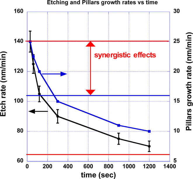
Etching rate and pillar growth rate vs time (error bars over five measurements). The red lines are the values of the sum of the chemical etching rate and physical sputtering estimated at the beginning and at the end of the process (20 min) (see Section 3, Discussion). The blue horizontal line is the contribution of the etching rate at the beginning obtained by applying the Flamm formula (see the text).
2.1.3. Surface Morphology by High-Resolution SEM
The evolution in surface morphology has been monitored from the HiRES SEM images taken at different process steps and is shown in Figure 4a (top views) and 4b (cross-sectional views). As shown in Figure 4a, at 30 s of the plasma process, an “island-like” morphology is visible, featuring a clusterized nanostructurization in a few areas and a low density of isolated nanostructures. After 60 s of etching, surface patterning becomes more homogeneous over the surface, although nanostructures are still quite small. The shape and height of nanostructures can be observed in SEM cross-sectional images and tilted views in Figure 4b. After 6 s of RIE, the height of the structures can be evaluated in the 10–40 nm range, while their shapes are not clearly defined yet.
Figure 4.

SEM images: (a) top view and (b) cross-section (left) and tilted (right) for samples obtained after 30 s, 1, 2, 5, 15, and 20 min of plasma processing.
After 2 min of RIE, nanostructures turn into pyramid-like pillars of defined morphology, although of uneven height, with an average value of about 40 nm tall and a few pillars exceed 100 nm. As RIE proceeds, patterning gains homogeneity in both pyramidal shape and height, and an average height of about 100 nm is reached (5 min of RIE). As the etching time is increased above 15 min, the pyramids start to widen at their bases as it is clearly visible in top-view and cross-sectional images of Figure 4b. For instance, after 15 and 20 min of etching, the pillars measure, respectively, 190 and 200 nm in height and about 80 and 100 nm in width at their bases. A pillar growth rate (nm/min) can therefore by estimated by dividing the pillar height, as estimated from the cross-section images, by the process time. Similar to the trend in the etching rate, the pillar growth rate also decreases with process time, with a halving time of about 20 min.
2.1.4. Surface Morphology by AFM
A better insight into the process of nanopatterning has been obtained by AFM inspection of the sample surface at 30 s, 60 s, 5 min, 15 min, and 20 min process times. Figure 5 reports the AFM morphological surface maps taken over a 5 × 5 μm2 probed area. A uniform growth of nanostructures can be directly appreciated, apart few exceptions.
Figure 5.

AFM topography images for samples obtained after 30 s, 1, 5, 10, 15, and 20 min of plasma processing.
2.1.5. Chemical Analysis on the Surface by XPS
XPS was performed to provide a chemical analysis of the textured Si surfaces after RIE processing. Survey and high-resolution spectra of C, F, Si, and O were acquired and then deconvolved to obtain information on the chemical species deposited. C, F, Si, and O were the only elements detected in the survey spectra. The evolution of C 1s, F 1s, Si 2p, and O 1s core-level lines with process time, along with their components, is presented in Figure 6a–d. By assigning a chemical species to each component of the fitting23−27 as presented in Table 1, it was possible to observe a shift in the binding energy (BE) of the species of the order of 0.2–0.3 eV at different times along the RIE process. Besides, it is well known that CFx and C–CF components are fingerprints of a fluoropolymer deposition, while SiFx components can only be the fingerprint of a chemical etching. There is also the presence of intermediate species Si–CO and SiC–OH throughout the process time. Although the levels of oxygen and silicon decrease progressively with time, the levels of carbon and fluorine increase. The relative concentration of each species has then been calculated by using the atomic sensitivity factor, and the respective trends are reported in Figure 7. As shown in Figure 7a, the ratio (SiF + SiF3)/(CF + CF2) increases almost linearly in time. More complex trends are instead shown by the ratios F/Si, C/Si, and F/C in Figure 7b and for the ratios SiF/Si, SiF3/Si and SiO2/Si in Figure 7c.
Figure 6.

Time evolution of core-line high-resolution spectra for: (a) C 1s, (b) F 1s, (c) Si 2p, and (d) O 1s.
Table 1. Identification of the Chemical Species to Each Contribution of the High-Resolution Core Lines Obtained with the Fitting.
| element | BE (eV) | BE (eV) | BE (eV) | BE (eV) | BE (eV) | BE (eV) |
|---|---|---|---|---|---|---|
| C 1s | 283.9 | 285.1 | 286.5 | 288 | 289.8 | 293.2 |
| C–C | C–O–Si | C-CF | CF | CF2 | CF3 | |
| Si 2p | 99.7 | 100.6 | 102.1 | 103.5 | ||
| Si | SiF/SiC | SiF3 | SiO2 | |||
| F 1s | 685.3 | 686.7 | 688.1 | 689.4 | ||
| SiF3 | SiF | C F2 | CF | |||
| O 1s | 531.5 | 532.7 | 534 | |||
| Si–COH | SiO2 | C–O–Si |
Figure 7.

Atomic concentration ratios as functions of plasma processing time (a) (SiF + SiF3)/(CF + CF2), (b) F/Si, C/Si and F/C, (c) SiF–SiC/S, SiF3/Si, and SiO2/Si. LFP: low-fluorine polymer growth regime following the definition in ref (32). See text below.
2.1.6. Chemical Analysis by ToF-SIMS
It is well known that SIMS technique is complementary to XPS for the ease of getting depth profiles and because it can reveal directly the presence of hydrogen. The mass spectra from the BSi samples obtained at different process times show the presence of variety of ions, molecular ions, and clusters such as SiO2–, SiO2F–, SiC–, SiCO–, C2F–CF–, CF2–, CF3–, Si3F–, CH–, C2H2, SiH–, H+, C2H+, C2H2+, SiHO+, SiOCs+, and Si ++, in addition to Al+, Na+, and F+, as surface contaminants. The surface chemical characterization is in agreement with the finding of XPS. In addition, ToF-SIMS spectra reveal the ions and molecules containing H and show the interaction of H2 with the surface.
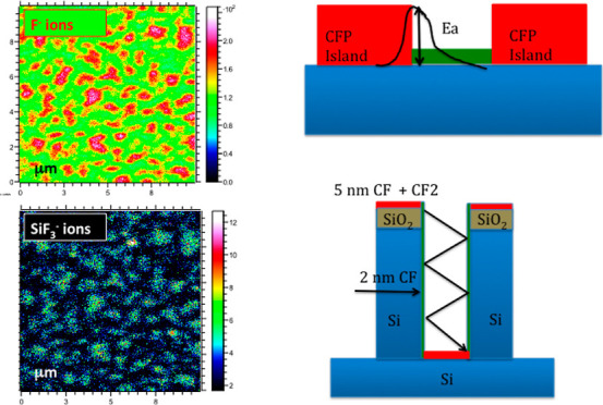
ToF-SIMS analyses of the two-dimensional spatial distribution of different species on the surface was performed in all samples over an area of 10 × 10 μm2. Figure 8 reports the results for the 20 min-treated sample, as SIMS maps of the F–,SiF3–, and CF2– signals, for an analyzed depth of 1–2 nm. The heterogeneous distribution of F-related signals reveals the presence of F-covered agglomerates of diameter 0.5–1.5 μm. Besides, the agglomerates of F– and SiF3– species are spatially coincident. In spite of the low sensitivity for the CF2 cluster, the spatial coincidence between map (c) and maps (a) and (b) can also be inferred. It has to be noticed that the presence of an island-like distribution of the fluorinated species becomes evident only in the 20 min treated sample due to limited spatial resolution of SIMS technique. Therefore non-uniform deposition of C–F species and heterogeneous surface chemistry, under the present experimental conditions, must occur right from the beginning ending with subsequent nanostructuring.
Figure 8.

ToF-SIMS images of the distribution of secondary ions from the surface of the 20 min-treated sample recorded from a 10 × 10 μm large area. (a) Distribution of F– ions (signal at mass 19 total count 8.662 × 10⁶), (b) distribution of SiF3– ions (signal at mass 103 total count 1.589 × 10⁵), and (c) distribution of CF2– ions (signal at mass 50 total count 8.396 × 10³).
ToF-SIMS depth profiling reveals the molecular structure of the pillars. Depth profiles for all samples were carried out using a 30 keV Bi+ beam for analysis and with a 2 keV Cs+ beam for sputtering.28Figure 9 shows a typical ToF-SIMS depth profile of the signals of the CF–, CF2–, and CF3– ions obtained for the BSi sample treated for 10 min. The sputtered depth is calculated from the sputtering rate measured on a reference sample. The CF–, CF2–, and CF3– signals are evidently originated from the region of nanopillars, showing that the pillars are covered with the C–F layer. On the top of the pillars, there is a layer about 4 nm thick enriched in CF2 and CF3 molecules, which can be recognized from high peaks in the CF2 and CF3 curves in Figure 9. The CF2 molecules may cover also a side wall of pillars as it can be inferred from the plateau of the CF2– signal in the depth region between 5 and 50 nm. The plateau in the CF2 signal at a depth of about 55 nm suggests that a deposition of this type of molecules may occur at the bottom of the valley. The CF– curve indicates a gradient concentration dependence of the CF– molecules along the pillar length. From the ToF-SIMS depth profile in Figure 9, the thickness of the pillar layer may be estimated to be about 80 nm, which roughly corresponds to that measured by SEM (120 nm). The difference may be attributed to the sputtering yield of the Cs+ ion beam on the Si–F–O–C mixed material, which may differ from that measured on the reference SiO2 material. In Table 2, we report the thickness of the C–F layers coating the pillars, as obtained from SIMS depth profiles similar to those shown in Figure 9. The CF layer reflects the thickness of the pillar layer since this species cover whole length of the pillar. The thickness of the CF2 top layer reflects the covering of the nanostructured surface. As such, one has to think that, once the ToF-SIMS starts to probe the surface at time 0, the CF2 detected is the sum of the contributions present at the top layer of the nanopillars and in the valleys in between.
Figure 9.
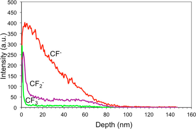
ToF-SIMS depth profile of the CF–, CF2–, and CF3– ions obtained on the BSi sample treated for 10 min. Only relevant signals are shown in the profile.
Table 2. Thickness of CxFy Layers Measured by ToF-SIMS Depth Profiling.
| treatment time (min) | F– (nm) | CF– (nm) overlayer | CF2– (nm) overlayer | layer (nm) by SEM |
|---|---|---|---|---|
| 0.5 | 3 | 2 | 0.5 | |
| 1 | 6 | 3 | 0.8 | |
| 2 | 19 | 5 | 3.5 | 40 |
| 5 | 46 | 17 | 3.9 | 100 |
| 10 | 78 | 32 | 4.2 | |
| 15 | 108 | 49 | 4.2 | 190 |
| 20 | 205 | 84 | 5.2 | 200 |
| 20 start-stop | 154.7 | 94 | 5.8 |
2.2. Procedure 2
In the second procedure, an RIE process 20 min long was run in a “start-and-stop”way, characterized by 1 min-long active time steps and intervals to exhaust the plasma created during the single time step before turning on the process again. This enabled us to monitor the reactive plasma via OES to check for a possible evolution in its composition that might affect surface nanostructurization.
2.2.1. Surface Morphology by AFM
Figure 10 shows the AMF topographic image of the sample obtained after a 20 min “start-and-stop” procedure, compared to what is obtained in samples exposed to a 15 min and a 20 min continuous RIE process (first procedure). The mean size of the nanostructures in the “start-and-stop” sample is comparable to that obtained in the 15 min case, whereas the heights are comparable to those obtained in the 20 min case.
Figure 10.

Comparison of AFM topography images among the start-and-stop test (left) and 15 min (center) and 20 min (right) continuous process times. One can immediately notice that the mean size for the start-and-stop case is in agreement with that of the 15 min case, while the height size is closer to that for the 20 min case.
2.3. Procedure 3
The third RIE procedure consisted in placing a reference Si specimen on a non-powered (grounded) electrode and comparing the results between powered and non-powered electrodes to check the definite role of ion sputtering in the formation of the nanostructures.
2.3.1. Morphology by High-Resolution SEM
Figure 11 shows SEM images of the surface morphology and cross-section of a sample placed on the grounded electrode and exposed to the reactive gas, after a 10 min-long RIE process at the same parameters as for the powered electrode case. Again, a portion of the sample was shielded from the RIE using a narrow strip of silicon (2 mm wide and 20 mm long) to compare treated and non-treated zones. In the composite cross-sectional view of Figure 11a, three different morphologies are noticeable in correspondence to three zones: the shielded area (left) shows a smooth Si surface, and the surface in the transition zone located at the edge of the mask (center) has an overall rough appearance, similar to that of the treated zone (right). Peak-to-peak roughness in the tens of nanometer range can be estimated. We speculate that in the transition zone, the silicon might have been locally etched with F atoms, able to leak in the gap between the mask and the silicon. The treated surface exhibited the same surface morphology, but in this case, a thin fluorocarbon layer might have grown and covered the roughened Si. The deposition of a fluorocarbon layer of a few tens of nanometer thick is actually confirmed from the SEM cross-sectional image of Figure 11b. The top view in Figure 11c refers to a region where nano-scratches in the cover film unveils the underlying roughened surface of the Si wafer.
Figure 11.

High-resolution SEM images of surface morphology of a Si sample exposed on the ground cathode and processed for 20 min. (a) Cleaved cross-sectional images refer respectively to a masked zone (left), showing a smooth polished surface of pristine Si wafers, to the transition zone (center), showing an increase in surface roughness, and to a coated region (right), again showing roughness of comparable quality. (b) Cross-section in the coated region, where the deposition of a layer a few tens of nanometer in thickness is evident. (c) Top-view image, showing the evident texturization of both the coated surface and of the Si underneath it.
3. Discussion
Since the intensity of the monitoring OES signals from the reactive plasma remains constant during the process time and similar surface morphologies are issued from the 20 min RIE process run in procedure n.1 (continuous) and n.2 (“start-and-stop”), we derive that the nanopatterning of Si is not ascribable to changes in plasma chemistry but merely to phenomena occurring on its surface. Therefore, our discussion will focus on the chemical and physical interactions of the species on and with the surface.
3.1. Etching Rate
The black solid line in Figure 3 plots the measured evolution in the etching rate with the duration of RIE. It is experimentally evident that the etching rate slows along the RIE process. Under 10% H2 in the plasma mixture, the etching rate measured at 10 min (80 nm/min) matches the results by Coburn.29 The present results can be discussed in the light of studies previously reported in the literature by assuming that the overall etching rate is contributed by both the chemical etching and the physical sputtering. The major contribution to the chemical etching is given by the neutral F atoms. Assuming a F concentration of 1015 cm–3, typical for the RIE process with CF4 plasma and a substrate temperature of 300 K, an etch rate of about 95 nm/min is obtained by applying the Flamm formula.30 With regard to the physical sputtering, it was demonstrated via mass spectrometry by Booth and co-workers that, in a pure CF4 plasma at 200 mTorr and 100 W, the two most abundant ionic species are CHF2+ and CF3+.31 They estimated a total ion flux at the powered electrode of the order of 8 × 1015 cm–2 s–1. On the other hand, Lejeune showed that for a CF4 plasma at much lower pressure (10–4 mbar), the predominant species is CF3+.32 With the only purpose to estimate the physical sputtering rate, we assume that the predominant species in our mixture is CF3+ and that the physical sputtering is given by this ionic species only. In our case, the ion flux could not be directly measured via a Langmuir probe due to the relatively high pressure. However, thanks to the above simplification, it can be estimated with the aid of the following formula suggested by Booth31
| 1 |
In eq 1, Pin is the power dissipated into the discharge, A is the power electrode area, Γion, is the ion flux, and Vbias is the dc self-bias of the electrode. Taking into consideration that the real power dissipated into the discharge is much lower than the input power, according to Booth,30,33 we can admit that Pin is about one-third of the input power. For a 200 W discharge at Vbias = 830 V and a round electrode of diameter equal to 10 cm, we have Γion = 6.06 × 1015 cm–2 s–1 or a current density of 0.96 mA cm–2. The simulation ran by Mayer and Barker34 at Vbias = 860 V gave a sputtering rate of less than 20 nm/min/(mA/cm2) and that in our case issues a value of ∼10 nm/min. The sum of the two factors accounts for a total etching rate of 105 nm/min at the onset of the process (reported as a straight blue line as a guide for the eye in Figure 3). The difference in reaching the experimental value is ascribed to synergistic effects typical of RIE processes.35,36
The similar functional trends shown by the temporal evolution in the etching rate and in the pillar growth rate, both reported in Figure 3, suggest that the decrease in the etching rate with process time merely proceeds from a change in surface chemistry and morphology. As a first guess, a very simple estimate can be carried out by looking at the increase in the actual surface area. As such, the final chemical etching contribution at the end of the process can be estimated simply by assuming a uniform growth of perfect cylindrical pillars of 200 nm height with a radius of 100 nm, which gives an increase in the exposed surface of 3.8 cm2 every cm2 of the initial sample surface, reducing the chemical etching to 19.7 nm/min. However, a more precise estimate must take into account the increase in the area covered by the passivation layer along the process time that reduces the chemical etching. The difficulties arise because there is no technique with the lateral resolution able to detect such small areas covered with the fluoropolymers.
The decrease in the physical sputtering rate with the pillar growth is not as straightforward to be evaluated as for the chemical etching. If only the decrease in the chemical etching rate is considered and by adding the same initial contribution for synergistic effects, the total etching rate at the end of the process is about 65 nm/min. This is indicated by the bottom red line in Figure 3. Generally speaking, one can say that the initial and final global etching rates are within the range estimated on the basis of available data and simplifications of the case. However, it is opinion of the authors that some values of the parameters used above may lead to overestimation of the etching rate. In fact, a concentration of the F neutral atoms of 1015 cm–3 refers to a pure CF4 plasma and does not take into account the scavenging effect of the H atoms for a CF4/H2 mixture to form HF neutrals. Finally, the pyramid-like shape of the pillars described in Section 3.1 is likely to increase the net surface area with respect to the cylindrical-shaped pillar used to estimate the increase in the surface area.
3.2. Evolution in the Chemical Composition on the Surface
3.2.1. XPS
The results of XPS characterization reveal that in addition to the CFx species, also C–O–Si, SiC, and C–C components are always present, meaning that both Si and SiO2 are continuously being etched. This suggests possible reactions like
| 2 |
| 3 |
to be always present during the process. However, the intensity of the O 1s core line decreases with the process time, corresponding to the sputtering away of SiO2 on the Si surface and suggesting that the contribution to O2 as impurities does not play a major role.
Regarding the evolution of the fluorocarbons, even though from Figures 4 and 7 one can deduce that fluorocarbons are continuously deposited during the process, it appears from Figure 7a that the coverage of the area etched with F increases with respect to that of the fluoropolymer (CFP) deposited. A further insight into the evolution of the process is provided by the atomic ratio F/C presented in Figure 7c. According to the classification by Marks,32 our process can be identified as starting with a low-fluorine polymer and ending as a true RIE process. However, our maskless process ends with an extremely high F/C ratio (about 1.5)34,37 (highly fluorinated polymer) with a low expected geometrical aspect ratio.
The chemical characterizations of silicon texturized with fluorocarbon gases previously reported in the literature are related to masked processes. For example, a rather comprehensive work was carried out by Joubert et al.,38−40 and our results show a substantial agreement with it, in terms of the chemical species identified therein.
Moreover, from the perspective to explain the grow mechanism in the maskless case, some further useful results have to be considered, albeit with the due reserve.
The first is that, given the fluorocarbon gas, the etching stops at a particular value of aspect ratios for the pillars. In a masked process, the chemical etching of F stops at the bottom of the holes because of the deposition of a thick fluoropolymer layer (≥5 nm).38−40 The proposed rationale is that as the etching proceeds and the aspect ratio increases, the loss in power density at the bottom of the features is such that the etching regime changes from chemical sputtering to fluorocarbon suppression and finally to a deposition regime. Since it is only a matter of aspect ratios, it is reasonable to think that the same rationale also holds for the present maskless process. Therefore, since structures with a more complex geometry are formed as the texturization proceeds, it is also reasonable to assume that the power density loss is higher in our case and therefore that the final aspect ratio is lower than that reported in refs (38)–40, as it is actually observed. Further tests, not reported here for brevity, with the total RIE process time extended to 30 min confirmed that the texturization did not proceed further than that reached in the 20 min case.
Second, in a masked process, the polymer deposition rate increases with the aspect ratio and is higher at the edge than at the center of contact holes. Etching stops because of the deposition of the fluorocarbon polymer, and it stops at the edge of the holes sooner than at their center. Such important results were obtained by using a charge neutralizer gun in the ON–OFF mode so that it was possible to separate the XPS signals coming from the photoresist surfaces and from the surface of the contact holes.36 Evidently, in the present case of maskless processes, the same procedure is not applicable. Nevertheless, a similar mechanism has to be invoked also in the present case in order to explain why the texturization proceeds up to the final aspect ratio.
It also needs to be noticed that a typical value for the practical effective attenuation length (EAL) λ of the Si2p electron in a fluoropolymer overlayer film, like Teflon, is about 4 nm41 and that XPS analysis probes over 3λ in depth. This means that it is not possible to clearly discern between a Si-free surface and the one covered with a 12 nm-thick overlayer of such a fluoropolymer. This, along with the fact that a fluoropolymer thickness of 2.5 nm still allows Si to be etched with F, suggests that the coverage of Si and SiO2 is with a fluoropolymer overlayer not thicker than 2.5 nm. This coverage increases with the process time by the etching of F. Figure 9c indicates that a transient regime sets on (2 min) before a steady state is reached. The occurrence of such transients is known and explained by the occurrence of non-linear phenomena where deposition and removal rates of CF by ion sputtering depend only on its thickness. When the dose of the predominant sputtering species is below 1017 cm–2, like in our case, etching of SiO2 with few nanometers of the C–F overlayer occurs.42,43
The distribution of the CF– and CF2– species along the depth profiles was provided by ToF-SIMS analysis.
As one can see from Table 2 CF2 never extends beyond 5 nm, while the CF– species seems almost distributed along the whole depth. Besides this, it is also worth noticing that the difference in the depth distribution is established starting from the case of the 5 min-long process and for longer cases.
3.3. Growth Model for the Onset of BSi Texturing
By combining the results from XPS and from ToF-SIMS analyses, a growth model for the BSi patterns is proposed. In Figure 12, a schematic representation of the chemistry of the structures at the end of the process is sketched by assuming for simplicity that regular cylindrical pillars are formed.
Figure 12.
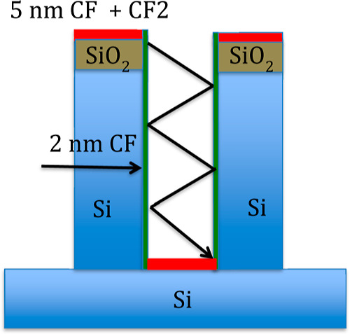
Schematic representation of the proposed growth model. On the top and valley of the structures, a rather thick film (red) of fluoropolymer blocks the chemical etching. Physical sputtering at the valleys ceases loss of energy by multiple reflections.
At the beginning, a fluoropolymer layer of CF and CF2 about 5 nm thick is deposited on the surface in the form of islands, as defined by the fluorocarbon deposition regime. Under the fluoropolymer islands, the chemical etching of Si or SiO2 with the F neutrals is stopped, while the thickness of the layer depends on the equilibrium between the rate of physical sputtering CF3+ and the rate of fluoropolymer deposition. Outside the islands, chemical etching and physical sputtering lead the texturization to proceed up to a defined aspect ratio. The lateral surface of the pillars may be covered with a thin layer of only 2 nm of CF, allowing the Si etching with F to proceed (fluorocarbon suppression regime).
The defined aspect ratio is reached at the point when the loss in density and energy of etching ions, caused by multiple reflections at the walls, is such that the physical sputtering of the fluoropolymer deposited on the valleys ceases. Again, a 5 nm-thick fluoropolymer layer of CF and CF2 is deposited on the valley too and chemical etching at the valleys stops.
A detailed study on the ion energy loss at the valley, which is necessary to observe the etch stop at high aspect ratios, can be found in ref (44). Even though the simulation reported therein refers to a masked process, once the morphology of the texturization is defined, the mechanism of ion energy and density loss at the bottom of the features proceeds, regardless of whether the process started masked or maskless, so that the same mechanism can be invoked to explain the etch stop.
By assuming this growth model, one can notice that conceptually there are no substantial differences between a maskless and a masked process. Therefore, we are left with the final point to be discussed, which is the mechanism of nucleation of thick fluoropolymer islands on the surface that triggers the maskless process. Based on the results of XPS and ToF-SIMS and on SEM images, which revealed that in the case of exposure on the grounded electrode, a uniform fluoropolymer film is deposited without any nanostructurization, we propose a scheme for the island formation on the surface, which is illustrated with the aid of Figure 13.
Figure 13.
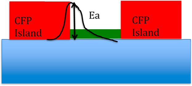
Schematic representation of the initial stage of growth of the structures. On the bare surface (green area), the activation energy (Ea) for surface mobility is too high and CFP radicals cannot diffuse to bridge the islands (red). As a consequence, both chemical etching and physical sputtering are active and the texturization starts.
The deposition of the fluoropolymer thin film starts by following a disordered island structure growth scheme (Wolmer–Weber type), as also shown in SEM images (Figure 4a, cases at 30 and 60 s). The coalescence stage, at which islands should merge to form a uniform film, is suppressed because of the induced effect of highly energetic ion sputtering that reduces the surface mobility of adsorbed species (lattice defects, ions implanted, and a-Si) by increasing its activation energy. At initial process times (<15 min, see Figure 7b), the chemical sputtering proceeds at different rates between polymer-covered and -uncovered areas. Starting from 15 min, what can be properly called the “RIE regime”, a polymer layer of 5 nm is formed and the nanostructurization ceases. In order to corroborate this rationale, we recall that Ekaterina invoked a passivating layer as well to trigger the nanostructurization of ultrablack silicon by RIE but using SF6 and O2 gases.45
3.4. Rationale for the Pyramid-like Shape of the Nanostructures
We ascribe the formation of this type of structure to the different effects of ion bombardment on the top and on the side walls of the growing nanostructures. In fact, the top of the pillars is exposed to the full angular distribution of the ion trajectories, whereas the side walls can be reached only by ions with trajectories closely perpendicular to the side walls. Therefore, since the sides of the structures are subjected to a less efficient ion sputtering, they become covered with a thicker CFx layer, so that the etching with F* is reduced. As the aspect ratio increases, the etching of the lower part of the structures becomes increasingly less efficient, resulting in a pyramidal shape. This also confirms the prevailing role of the F radical and thus of the etching process within the first few minutes.
The pyramid structure permits also to explain the reduced reflectivity typically observed with BSi, Figure 14. The reflectivity curves measured from unprocessed Si wafers and BSi wafers are presented in Figure 14a. A simple cascaded-matrix model was used to calculate the optical reflectivity of the wafer in the visible and near-infrared range. The pyramid structure on a semi-infinite Si substrate was modeled using the effective medium approximation,46 considering that the dimensions of the nanostructure are smaller than the wavelength of interest. The corresponding calculated curves are presented in Figure 14b, where significant reduction in reflectivity is observed when the Si multilayer includes a layer whose effective index represents 200 nm-high pyramids, qualitatively reproducing the experimental results. A more detailed optical modeling of the geometrically non-regular nano-structured layer obtained with a maskless process would require a sophisticated and time-consuming numerical analysis. On the other hand, the simple method considered here permits the assessment of the reflectivity by varying the layer thickness, obtaining a qualitatively satisfactory representation of the structure of interest.
Figure 14.

Reflectivity (a) measured at different etching process durations and (b) reproduced by a simple cascaded-matrix optical model considering 200 nm-high pyramids: unprocessed Si wafer reflectivity (green) and BSi wafers (red).
4. Conclusions
Black silicon samples have been obtained by a maskless RIE process using a CF4 + 10% H2 gas mixture with 200 W RF power. In order to elucidate the mechanism of surface nanopatterning, three different exposure procedures have been run, and their results have been compared. The first procedure consisted in exposing the samples to the reactive plasma for different times up to a maximum of 20 min. The second one consisted in treating the samples for 20 min altogether, but stepwise, 1 min at a time and pumping away the exhausted mixture at the end of each time step while keeping the same process parameters at each step. The purpose of the second procedure was to avoid exposure to reactive species possibly formed by the plasma–surface interactions that could themselves contribute to the nanopatterning process. The third procedure consisted in exposing a sample placed over the grounded electrode for 20 min, under the same parameters as of the first procedure, in order to remove the etching contribution due to the physical sputtering of the accelerated ions. AFM results on samples exposed via the first and second procedure showed the same morphology. This fact, along with the OES results, allowed us to say that there were no changes in the plasma chemistry during the treatment, which could contribute to the change in surface morphology during the nanostructurization.
Therefore, we could focus our attention only to what occurred on the surface of the samples at different process times. A thorough investigation by SEM, AFM, XPS, and ToF-SIMS suggested that surface texturing in a maskless process proceeds and ceases via the same mechanisms as for a masked process, provided one can explain the mechanism of initial formation of the islands of fluoropolymers, which eventually trigger the nanostructurization.
Combining the XPS and ToF-SIMS results, we propose that CF and CF2 islands of fluoropolymers about 5 nm thick are initially deposited in a Wolmer-Weber-type scheme. Such a thickness is sufficient to stop the fluorine chemical etching of silicon on the surface below the islands, while on the free silicon surface, chemical etching and physical sputtering are very effective and nanostructurization can take place. Meanwhile, the energetic ions impinging on the free silicon surface could induce a high enough density of surface defects to increase the activation energy for surface diffusion of CF and CF2 species, thus preventing coalescence and the formation of a uniform fluoropolymer layer. Instead, the SEM inspection clearly showed that in the case of silicon samples exposed on the grounded electrode, a thin uniform layer is formed and no nanostructurization took place.
The net process is of erosion. The erosion is due to three contributions. One is due to chemical etching, one due to physical sputtering, and one due to the synergistic effect by the plasma. The erosion rate and the pillar growth rate decrease rapidly with time. Thanks to the fact that the plasma chemistry does not change during the exposures, one can assume the contribution of synergistic effects to remain unvaried. A simple estimate of the final etching rate was carried out by evaluating a decrease in the chemical etching rate due to the increase in the surface area because of the growth of the nanopillars. The addition of a constant contribution of synergistic effects leads to estimation of a final erosion rate that is in accordance with the experimentally measured value. This further corroborates the model proposed where physical sputtering ceases at the end of the process. As time increases along the process, the shape of nanopillars deviates from cylindrical to pyramid-like. This can be explained on a simple rationale based on the different ion bombardment effects on the top and on the side walls of the growing nanostructures. Present findings contribute detailed knowledge of the mechanisms that rule maskless RIE patterning of black silicon surfaces, therefore providing a tool in view of fully mastering and exploiting the process.
5. Experimental Section/Methods
5.1. Experimental Apparatus
An RF plasma system47 was used to produce a physical structuring of silicon (type P, dopant B, ⟨100⟩, 0.01–0.02 Ω cm, 1 × 1 cm2, and thickness = 400 μm). The experimental apparatus consists of a parallel plate, capacitive-coupled system, in a cylindrical stainless-steel vacuum chamber with an asymmetric electrode configuration. The powered electrode (3 in. diameter) was connected to an RF (13.56 MHz) power supply, coupled with an automatic impedance matching unit, while the other stainless-steel electrode (3 in. diameter) was grounded. Si substrates were placed on the powered electrode at 6 cm away from the ground electrode. Before starting the process, the Si samples were cleaned with ethanol and dried with dry compressed air to remove surface contaminants. The process chamber was pumped to a base pressure below 1 × 10⁻⁵ Pa; then, high-purity CF4 (99.9%) and H2 (99.99%) gases (10% H2) were introduced into the chamber using a mass flow controller to achieve the desired working pressure, which was fixed at 9 Pa.
5.2. Methodology
In order to understand whether the nanostructuring depends exclusively on the surface morphology or also on the formation of new reactive species in the plasma phase, created by the interaction with the surface, two different experimental procedures were followed to study the effects of the plasma chemistry on the growth of the nanostructures. The first one was to treat the Si surface with the plasma continuously at different exposure times (0.5, 1, 2, 5, 15, and 20 min). The second one was to expose the Si surface to the plasma for a net total time of 20 min but with cycling between 1 min of plasma treatment and 1 min of pumping of the exhaust mixture (start-and-stop test). In this second case, it was possible to remove the reactive species formed in the plasma phase before regenerating the plasma. Then, by comparing the samples obtained from the two procedures, it was possible to discern whether a possible change in the species in the plasma phase can contribute to the nanostructurization process. The 1 min plasma exposure time was chosen as a good compromise between the time needed to start up the plasma operation and the time where neither the surface morphology nor the chemistry on the surface reached a steady state. Of course, the choice was made upon the SEM and XPS results on the samples exposed with the first procedure (see discussion below). The 1 min pumping time was adopted for the pressure in the RIE chamber to reach a base pressure of 10–2 to 10–3 Pa during pumping of the exhaust mixture, after starting from a value of initial pressure of 9 Pa.
A third procedure was also used to show that the onset of the nanostructures is triggered by the energetic ions reaching the powered electrode. The procedure consisted in exposing a sample placed over the grounded electrode for 10 min under the same parameters as of the first procedure and comparing the respective morphologies. We did not exceed 10 min of process in order to avoid possible delamination of the polymeric film.
5.3. Diagnostics
The plasma phase was characterized by OES.
The samples were characterized by SEM, AFM, surface profilometry, XPS, and ToF-SIMS.
Author Contributions
F.G. is the first author. He carried out the XPS measurement, collaborated in the ToF-SIMS measurements, and drafted the manuscript. S.M.P. carried out the SEM measurement and collaborated in the discussion and revision of the manuscript. M.P. carried out the sample deposition and AFM measurements and collaborated in drafting of the manuscript. R.C. helped in the sample preparation and revision of the manuscript. A.C. carried out the OES measurements. F.C. carried out the software simulation, suggested the start and stop procedure and helped with the revision of the manuscript. J.K. carried out the ToF-SIMS measurements and collaborated in the discussion. E.V. collaborated in the sample preparation and optical measurements. M.A. was involved in the results and discussion and revision of the manuscript.
The authors declare no competing financial interest.
References
- Koynov S.; Brandt M. S.; Stutzmann M. Black thin film silicon. J. Appl. Phys. 2011, 110, 043537–043547. 10.1063/1.3626900. [DOI] [Google Scholar]
- Steglich M.; Lehr D.; Ratzsch S.; Käsebier T.; Schrempel F.; Kley E.-B.; Tünnermann A. An ultra-black silicon absorber. Laser Photonics Rev. 2014, 8, L13–L17. 10.1002/lpor.201300142. [DOI] [Google Scholar]
- Sai H.; Kanamori Y.; Arafune K.; Ohshita Y.; Yamaguchi M. Light Trapping Effect of Submicron Surface Textures in Crystalline Si Solar Cells. Prog. Photovoltaics 2007, 415–423. 10.1002/pip.754. [DOI] [Google Scholar]
- Savin H.; Repo P.; von Gastrow G.; Ortega P.; Calle E.; Garín M.; Alcubilla R. Black silicon solar cells with interdigitated back-contacts achieve 22.1% efficiency. Nat. Nanotechnol. 2015, 10, 624–628. 10.1038/nnano.2015.89. [DOI] [PubMed] [Google Scholar]
- Halbwax M.; Sarnet T.; Delaporte P.; Sentis M.; Etienne H.; Torregrosa F.; Vervisch V.; Perichaud I.; Martinuzzi S. Micro and nano-structuration of silicon by femtosecond laser: Application to silicon photovoltaic cells fabrication. Thin Solid Films 2008, 516, 6791–6795. 10.1016/j.tsf.2007.12.117. [DOI] [Google Scholar]
- Yoo J. S.; Parm I. O.; Gangopadhyay U.; Kim K.; Dhungel S. K.; Mangalaraj D.; Yi J. Black silicon layer formation for application in solar cells. Sol. Energy Mater. Sol. Cells 2006, 90, 3085–3093. 10.1016/j.solmat.2006.06.015. [DOI] [Google Scholar]
- Ivanova E. P.; Hasan J.; Webb H. K.; Gervinskas G.; Juodkazis S.; Truong V. K.; Wu A. H. F.; Lamb R. N.; Baulin V. A.; Watson G. S.; Watson J. A.; Mainwaring D. E.; Crawford R. J. Bactericidal activity of black silicon. Nat. Commun. 2013, 4, 2838–2844. 10.1038/ncomms3838. [DOI] [PMC free article] [PubMed] [Google Scholar]
- Roumanie M.; Delattre C.; Mittler F.; Marchand G.; Meille V.; Debellefon C.; Pijolat C.; Tournier G.; Pouteau P. Enhancing surface activity in silicon microreactors: Use of black silicon and alumina as catalyst supports for chemical and biological applications. Chem. Eng. J. 2008, 135, S317–S326. 10.1016/j.cej.2007.07.053. [DOI] [Google Scholar]
- Wu C.; Crouch C. H.; Zhao L.; Carey J. E.; Younkin R.; Levinson J. A.; Mazur E.; Farrell R. M.; Gothoskar P.; Karger A. Near-unity below-band-gap absorption by microstructured silicon. Appl. Phys. Lett. 2001, 78, 1850–1852. 10.1063/1.1358846. [DOI] [Google Scholar]
- Huang Z.; Geyer N.; Werner P.; de Boor J.; Gösele U. Metal-Assisted Chemical Etching of Silicon: A Review. Adv. Mater. 2011, 23, 285–308. 10.1002/adma.201001784. [DOI] [PubMed] [Google Scholar]
- Ma L. L.; Zhou Y. C.; Jiang N.; Lu X.; Shao J.; Lu W.; Ge J.; Ding X. M.; Hou X. Y. Wide-band “black silicon” based on porous silicon. Appl. Phys. Lett. 2006, 88, 171907–171909. 10.1063/1.2199593. [DOI] [Google Scholar]
- Jansen H.; Gardeniers H.; Boer M. d.; Elwenspoek M.; Fluitman J. A survey on the reactive ion etching of silicon in microtechnology. J. Micromech. Microeng. 1996, 6, 14–28. 10.1088/0960-1317/6/1/002. [DOI] [Google Scholar]
- Nositschka W. A.; Voigt O.; Manshanden P.; Kurz H. Texturisation of multicrystalline silicon solar cells by RIE and plasma etching. Sol. Energy Mater. Sol. Cells 2003, 80, 227–237. 10.1016/j.solmat.2003.06.003. [DOI] [Google Scholar]
- Oehrlein G. S.; Rembetski J. F.; Payne E. H. Study of sidewall passivation and microscopic silicon roughness phenomena in chlorine-based reactive ion etching of silicon trenches. J. Vac. Sci. Technol., B: Microelectron. Process. Phenom. 1990, 8, 1199–1211. 10.1116/1.584896. [DOI] [Google Scholar]
- Jansen H.; de Boer M.; Legtenberg R.; Elwenspoek M. The black silicon method: a universal method for determining the parameter setting of a fluorine-based reactive ion etcher in deep silicon trench etching with profile control. J. Micromech. Microeng. 1995, 5, 115–120. 10.1088/0960-1317/5/2/015. [DOI] [Google Scholar]
- Liu X.; Coxon P. R.; Peters M.; Hoex B.; Cole J. M.; Fray D. J. Black silicon: fabrication methods, properties and solar energy applications. Energy Environ. Sci. 2014, 7, 3223–3263. 10.1039/c4ee01152j. [DOI] [Google Scholar]
- Cheng P.; Wang H.; Müller B.; Müller J.; Wang D.; Schaaf P. Photo-Thermoelectric Conversion Using Black Silicon with Enhanced Light Trapping Performance far beyond the Band Edge Absorption. ACS Appl. Mater. Interfaces 2021, 13, 1818–1826. 10.1021/acsami.0c17279. [DOI] [PubMed] [Google Scholar]
- Cheng P.; Wang H.; Wang H.; Aken P. A.; Wang D.; Schaaf P. High-Efficiency Photothermal Water Evaporation using Broadband Solar Energy Harvesting by Ultrablack Silicon Structures. Adv. Energy Sustainability Res. 2021, 2, 2000083. 10.1002/aesr.202000083. [DOI] [Google Scholar]
- Oehrlein G. S.; Williams H. L. Silicon etching mechanisms in a CF4/H2 glow discharge. J. Appl. Phys. 1987, 62, 662–672. 10.1063/1.339766. [DOI] [Google Scholar]
- Dussart R.; Mellhaoui X.; Tillocher T.; Lefaucheux P.; Volatier M.; Socquet-Clerc C.; Brault P.; Ranson P. Silicon columnar microstructures induced by an SF6/O2 plasma, J. Phys. D. Appl. Phys. 2005, 38, 3395–3402. 10.1088/0022-3727/38/18/012. [DOI] [Google Scholar]
- Vassallo E.; Pedroni M.; Pietralunga S. M.; Caniello R.; Cremona A.; Di Fonzo F.; Ghezzi F.; Inzoli F.; Monteleone G.; Nava G.; Spampinato V.; Tagliaferri A.; Zani M.; Angella G. Black-silicon production process by CF4/H2 plasma. Thin Solid Films 2016, 603, 173–179. 10.1016/j.tsf.2016.02.008. [DOI] [Google Scholar]
- d′Agostino R.; Cramarossa F.; De Benedictis S.; Ferraro G. Spectroscopic diagnostics of CF4-O2 plasmas during Si and SiO2 etching processes. J. Appl. Phys. 1981, 52, 1259–1265. 10.1063/1.329748. [DOI] [Google Scholar]
- Bodas D. S.; Mandale A. B.; Gangal S. A. Deposition of PTFE thin films by RF plasma sputtering on {100} silicon substrate. Appl. Surf. Sci. 2005, 245, 202–207. 10.1016/j.apsusc.2004.10.023. [DOI] [Google Scholar]
- Pereira J.; Pichon L. E.; Dussart R.; Cardinaud C.; Duluard C. Y.; Oubensaid E. H.; Lefaucheux P.; Boufnichel M.; Ranson P. In situ x-ray photoelectron spectroscopy analysis of SiOxFy passivation layer obtained in a SF6/O2 cryoetching process. Appl. Phys. Lett. 2009, 94, 071501–071503. 10.1063/1.3085957. [DOI] [Google Scholar]
- Coyle G. J. Jr.; Oehrlein G. S. Formation of a silicon-carbide layer during CF4/H2 dry etching of Si. Appl. Phys. Lett. 1985, 47, 604–606. 10.1063/1.96086. [DOI] [Google Scholar]
- McFeely F. R.; Morar J. F.; Shinn N. D.; Landgren G.; Himpsel F. J. Synchrotron photoemission investigation of the initial stages of fluorine attack on Si surface: Relative abundance of fluorosilyl species. Phys. Rev. B Matter Mater. Phys. 1984, 30, 764–770. 10.1103/physrevb.30.764. [DOI] [Google Scholar]
- Gottlieb S. O.; Lee Y. H. Reactive ion Etching related Si surface residues and subsurface damage: Their relationship to fundamental etching mechanisms. J. Vac. Sci. Technol., A 1987, 5, 1585–1594. [Google Scholar]
- Scarazzini R.ToF-SIMS characterisation of fragile materials used in microelectronic and microsystem devices : validation and enhancement of the chemical information. Chemical Physics, PhD Thesis; Université Grenoble Alpes, 2016. https://tel.archives-ouvertes.fr/tel-01488629. [Google Scholar]
- Coburn J. W.; Winters H. F. Plasma etching—A discussion of mechanisms. J. Vac. Sci. Technol. 1979, 16, 391–403. 10.1116/1.569958. [DOI] [Google Scholar]
- Fridman A.. Plasma chemistry; Cambridge University Press, 2008, p 524. online ISBN: 9780511546075.. [Google Scholar]
- Booth J.-P. Optical and electrical diagnostics of fluorocarbon plasma etching processes. Plasma Sources Sci. Technol. 1999, 8, 249–257. 10.1088/0963-0252/8/2/005. [DOI] [Google Scholar]
- Lejeune C.; Grandchamp J. P.; Gilles J. P.; Collard E.; Scheiblin P. Reactive ion beam etching of silicon with a new plasma ion source operated with CF4 : SiO2 over Si selectivity and Si surface modification. Rev. Phys. Appl. 1989, 24, 295–308. 10.1051/rphysap:01989002403029500. [DOI] [Google Scholar]
- Booth J. P.; Cunge G.; Sadeghi N.; Boswell R. W. The transition from symmetric to asymmetric discharges in pulsed 13.56 MHz capacitively coupled plasmas. J. Appl. Phys. 1997, 82, 552–560. 10.1063/1.365614. [DOI] [Google Scholar]
- Marks J.; Collins K.; Yang C. L.; Groechel D.; Keswick P. R.; Cunningham C.; Carlson M. Carlson Introduction of a new high-density plasma reactor concept for high-aspect-ratio oxide etching. Proc. SPIE 1993, 1803, 235–247. 10.1117/12.142917. [DOI] [Google Scholar]
- Coburn J. W.; Winters H. F. ION- and electron-assisted gas-surface chemistry-An important effect in plasma etching. J. Appl. Phys. 1979, 50, 3189–3196. 10.1063/1.326355. [DOI] [Google Scholar]
- Marchack N.; Chang J. P. Perspectives in nanoscale plasma etching: what are the ultimate limits?. J. Phys. D: Appl. Phys. 2011, 44, 174011. 10.1088/0022-3727/44/17/174011. [DOI] [Google Scholar]
- Cardinaud C.; Rhounna A.; et al. Analyse XPS des surfaces de Si et SiO2 exposées aux plasmas de CHF3 et CHF3-C2F6. Polymérisation et gravure” ev. Phys. Appl. 1989, 24, 309–321. 10.1051/rphysap:01989002403030900. [DOI] [Google Scholar]
- Joubert O.; Czuprynski P.; Bell F. H.; Berruyer P.; Blanc R. Analyses of the chemical topography of silicon dioxide contact holes etched in a high density plasma source. J. Vac. Sci. Technol., B: Microelectron. Nanometer Struct.--Process., Meas., Phenom. 1997, 15, 629–639. 10.1116/1.589305. [DOI] [Google Scholar]
- Joubert O.; Oehrlein G. S.; Zhang Y. Fluorocarbon high density plasma. V. Influence of aspect ratio on the etch rate of silicon dioxide in an electron cyclotron resonance plasma. J. Vac. Sci. Technol., A 1994, 12, 658–664. 10.1116/1.578849. [DOI] [Google Scholar]
- Joubert O.; Oehrlein G. S.; Surendra M. Fluorocarbon high density plasma. VI. Reactive ion etching lag model for contact hole silicon dioxide etching in an electron cyclotron resonance plasma. J. Vac. Sci. Technol., A 1994, 12, 665–670. 10.1116/1.578850. [DOI] [Google Scholar]
- NIST Electron effective Attenuation Length Database.
- Hori M.Plasma-material Interactions Diagnostics and Control Plenary Lecture ICPIG, 2017; Estoril: Portugal.
- Ohya Y.; Tomura M.; Ishikawa K.; Sekine M.; Hori M. Formation of a SiOF reaction intermixing layer on SiO2 etching using C4F6/O2/Ar plasmas. J. Vac. Sci. Technol., A 2016, 34, 040602–040605. 10.1116/1.4949570. [DOI] [Google Scholar]
- Arnold J. C.; Sawin H. H. Charging of pattern features during plasma etching. J. Appl. Phys. 1991, 70, 5314–5317. 10.1063/1.350241. [DOI] [Google Scholar]
- Ekaterina A.; et al. Study of Cryogenic Unmasked Etching of “Black Silicon” with Ar Gas Additives”. ACS Omega 2022, 7, 6053–6057. 10.1021/acsomega.1c06435. [DOI] [PMC free article] [PubMed] [Google Scholar]
- Ravindra N. M.; Marti S. R.; Sekri S. Modelling of Optical Properties of Black Silicon/Crystalline Silicon. J. Sci. Ind. Metrol. 2015, 1, 1–7. 10.21767/2472-1948.100001. [DOI] [Google Scholar]
- Koenig H. R.; Maissel L. I. Application of RF discharges to sputtering. J. Res. Dev. 1970, 14, 106–110. 10.1147/rd.142.0168. [DOI] [Google Scholar]