Abstract
Vanadium dioxide (VO2) is one of the extensively studied strongly correlated oxides due to its intriguing insulator–metal transition near room temperature. In this work, we investigated temperature-dependent nanoscale conduction in an epitaxial VO2 film grown on an Al2O3 substrate using conductive-atomic force microscopy (C-AFM). We observed that only the regions near the grain boundaries are conductive, producing intriguing donut patterns in C-AFM images. Such donut patterns were observed in the entire measured temperature range (300–355 K). The current values near the grain boundaries increased by approximately two orders of magnitude with an increase in the temperature, which is consistent with the macroscopic transport data. The spatially-varied conduction behavior is ascribed to the coexistence of different monoclinic phases, i.e., M1 and M2 phases, based on the results of temperature-dependent Raman spectroscopy. Furthermore, we investigated the conduction mechanism in the relatively conductive M1 phase regions at room temperature using current–voltage (I–V) spectroscopy and deep data analysis. Bayesian linear unmixing and k-means clustering showed three distinct types of conduction behavior, which classical C-AFM cannot resolve. We found that the conduction in the M1 phase regions can be explained by the Poole–Frenkel mechanism. This work provides deep insight into IMT behavior in the epitaxial VO2 thin film at the nanoscale, especially the coexistence and evolution of the M1 and M2 phases. This work also highlights that I–V spectroscopy combined with deep data analysis is very powerful in investigating local transport in complex oxides and various material systems.
We investigated temperature-dependent nanoscale conduction in an epitaxial VO2 film grown on an Al2O3 substrate using conductive-atomic force microscopy and deep data analysis.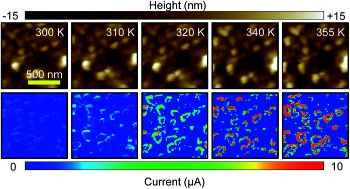
1. Introduction
Since its discovery in 1959,1 vanadium dioxide (VO2) has been an extensively studied strongly correlated oxide due to its intriguing insulator–metal transition (IMT). Its IMT temperature is very close to room temperature (at approximately 340 K in bulk single crystal) and drastic changes in electrical conductivity and optical properties are shown across the IMT. Therefore, VO2 has also attracted considerable interest in applications such as thermal sensors, smart windows, and memristive devices.2–5 An interesting characteristic of the IMT of VO2 is its accompanying structural phase transition (SPT), i.e., from a low-temperature insulating monoclinic phase (M1) to a high-temperature metallic rutile (R) phase. However, the concurrent occurrence of SPT has created a long-standing debate over the underlying mechanism of IMT. Namely, there has not been a consensus whether the primary mechanism of IMT of VO2 is an electron–electron interaction (Mott transition)6,7 or an electron–phonon interaction (Peierls transition).8,9 Mott-assisted Peierls pictures (i.e., both physics are important) have been recently proposed.10,11
Spatially-resolved mapping of local conductance change during IMT can provide deep insight into the IMT of VO2. Scanning probe microscopy (SPM) is a powerful technique because it allows real-space imaging of various physical properties at the nanoscale. Scanning near-field infrared microscopy12–14 and Kelvin probe force microscopy15,16 have been intensively used to study the IMT of VO2. In this respect, conductive-atomic force microscopy (C-AFM) can be the most powerful SPM technique because it directly measures local electrical conductance with a sub-nanometer spatial resolution.17–19 Recently, Kim et al. studied the IMT behavior in a granular polycrystalline VO2 film grown onto a Si substrate using temperature-dependent C-AFM.18 They observed local conductance differences inside a single grain during IMT, i.e., insulating grain cores and conductive grain boundaries, producing intriguing donut patterns in the C-AFM images. Based on temperature-dependent Raman spectroscopy results, they found that the donut-like conductance pattern is ascribed to the coexistence of relatively conductive M1 phase and insulating different monoclinic phase, the so-called M2 phase.
Note that the M2 phase is an intermediate state between the M1 and R phases. It has been experimentally observed during the transition from M1 to R phases.20–22 It is known that the M2 phase is formed by strain18,20–24 or doping.25,26 Therefore, the epitaxial strain induced by lattice mismatch between a film and a substrate could significantly affect the formation and evolution of the intermediate M2 phase and the resultant IMT. However, direct mapping of temperature-dependent nanoscale conductance change in the epitaxial VO2 films using C-AFM has rarely been performed.
Furthermore, the C-AFM allows current–voltage (I–V) spectroscopy measurement on a grid of multiple nanometer-sized points.27,28 It records the bias-induced current responses of the sample at each location, yielding spatially-resolved multidimensional data sets. The deep data analysis, such as k-means clustering29 and Bayesian linear unmixing,30 can be applicable to such multidimensional I–V data sets and provide an underlying mechanism of local conduction.31,32 This statistical approach combined with I–V spectroscopy can provide further insight into nanoscale conduction in materials. However, it has yet to be applied in VO2 films.
In this work, we investigated temperature-dependent nanoscale conduction behavior in an epitaxial VO2 thin film using C-AFM. We also observed similar donut patterns in the C-AFM images, as reported by Kim et al.,18 indicating that only the regions near the grain boundaries are conductive. However, unlike the previous report,18 the donut patterns were observed for the entire measured temperature range (300–355 K) in our epitaxial VO2 film grown on c-plane Al2O3 (c-Al2O3) substrate. This indicates that the M1 and M2 phases coexist even at room temperature due to the epitaxial strain induced by the c-Al2O3 substrate. Their coexistence was confirmed by temperature-dependent Raman spectroscopy. Furthermore, we investigated the local conduction mechanism in relatively conductive M1 phase regions using I–V spectroscopy and deep data analysis.
2. Materials and methods
The 20 nm-thick VO2 film was deposited on the c-Al2O3 substrate by using aerosol-assisted chemical vapor deposition.33 A precursor solution of 0.01 M concentration was prepared by dissolving vanadyl acetylacetonate (the source material for V ion) in 2-methoxyethanol. An aerosol of the precursor solutions was ultrasonically produced in a glass vessel and transported with Ar carrier-gas to a reaction chamber in which pyrolysis of the chemical vapor occurred on a heated substrate to produce a solid film. The temperature of the substrate holder was maintained at 420 °C during the film deposition. To examine the epitaxial relationship of VO2 film, high-resolution X-ray diffraction (HRXRD) θ–2θ, ϕ scans, and reciprocal space mapping (RSM) were performed using the X-ray diffractometer with a Cu target X-ray tube (D8 Discover, Bruker). Electrical transport property was investigated by measuring temperature-dependent resistance using four-probe method. For Raman spectroscopy measurements, a diode-pumped solid state laser with an excitation wavelength of 514.4 nm was used. The laser power was maintained at ∼0.3 mW during measurements to minimize local heating. The size of the laser spot was 1 μm2. The scattered Raman signal was dispersed using a Jobin-Yvon Horiba iHR550 spectrometer (2400 grooves per mm) and detected using a charge-coupled device. Temperature-dependent C-AFM was performed using a commercial atomic force microscope (NX-10, Park Systems) with a heating stage and a variable gain low noise current amplifier (DLPCA-200, Femto). Conductive Pt/Cr-coated AFM tips (ElectriTap190-G, BudgetSensors) with their spring constants of approximately 48 N m−1 were used for C-AFM imaging and I–V spectroscopy.
3. Results and discussion
3.1. Epitaxial relationship of the VO2 thin film
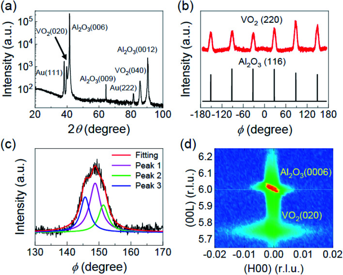
We verified from the results of HRXRD θ–2θ and ϕ scans that the VO2 thin film was epitaxially grown on c-Al2O3 (0001) substrate. As shown in Fig. 1(a), only sharp VO2 (020) and (040) peaks were observed at 2θ ≈ 39.8° and 85.6°, respectively, except for the Al2O3 substrate peaks and the Au peaks that originated from an Au electrode for C-AFM measurement, as described below. This θ–2θ scan result demonstrates that the (010)-faceted epitaxial VO2 layer was grown along the out-of-plane direction. We note that crystallographic (hkl) notation for VO2 is based on the monoclinic structure. To check further in-plane epitaxial alignment between the VO2 film and the c-Al2O3 substrate, HRXRD ϕ scan was performed. As shown in Fig. 1(b), the azimuth angles of six-fold VO2 (220) peaks with 60° separations match well with those of the six-fold Al2O3 (116) peaks with hexagonal symmetry due to their three equivalent domains, which is consistent with the ϕ scan results of other epitaxial VO2 films grown on c-Al2O3 substrates.34,35 This result demonstrates the perfect epitaxial relationship between the VO2 thin film and Al2O3 substrate.34 It is worth noting that the VO2 peaks in the ϕ scan are relatively broad. We found that each main peak has two small satellite peaks located at both sides with ∼2.6° angle deviation [Fig. 1(c)]. It has been reported that these satellite peaks originate from the intrinsic angle mismatch between the monoclinic β angle (122.6°) of VO2 film and the 120° of Al2O3 substrate hexagon.35,36Fig. 1(d) shows that the RSM was recorded around Al2O3 (0006) and VO2 (020) peaks. The broadness of the VO2 peak along the x-axis is comparable to that of the Al2O3 substrate peak, implying that our VO2 thin film exhibits a good crystallinity.
Fig. 1. (a) HRXRD θ–2θ scan and (b) ϕ scan of the VO2 film on the Al2O3 substrate at room temperature. (c) Enlarged ϕ scan near the VO2 film peak. Two satellite peaks of the VO2 (220) peak are observed, as displayed by the Lorentzian curve fitting lines. (d) RSM around Al2O3 (0006) and VO2 (020) peaks.
3.2. Macroscopic IMT and SPT behaviors
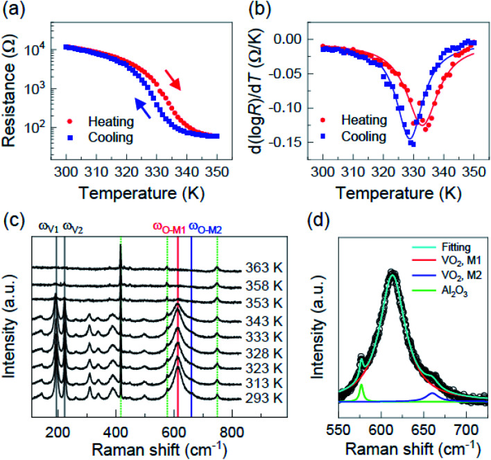
To study macroscopic IMT and SPT behaviors, we measured electrical resistance and crystal structure of VO2 film, respectively, at various temperatures. Fig. 2(a) shows the temperature-dependent electrical resistance of the VO2 film. The resistance–temperature (R–T) curve demonstrates a typical IMT behavior. The resistance ratio, R(350 K)/R(300 K), across the IMT is approximately 200. The IMT temperatures (TIMT) during heating and cooling are 333 K and 329 K, respectively, which was determined by fitting the Lorentzian curves to d(log R) versus T plots [Fig. 2(b)]. We performed temperature-dependent Raman spectroscopy to study SPT. Four phonon modes, ωV1, ωV2, ωO-M1, and ωO-M2, marked by the vertical solid lines in Fig. 2(c), are good indicators for the SPT of VO2.37 The two peaks in the low-frequency region (i.e., ωV1 and ωV2) are related to the vibration of V–V dimers. Additionally, the peaks around 610 cm−1 originate from the V–O lattice bonding. This V–O peak is considered the sum of two phonon modes, ωO-M1 and ωO-M2, related to the M1 and M2 phases of VO2, respectively.20,21,37 The intensities of the aforementioned four peaks decreases with increasing temperature [Fig. 2(c)]. They decrease drastically between 343 K and 353 K and totally disappear above 363 K, indicating SPT occurrence. This difference between IMT and SPT temperatures suggests that our VO2 film undergoes a Mott-type IMT. We found from the deconvoluted Raman spectrum of the V–O peak that the M1 and M2 phases coexist even at room temperature [Fig. 2(d)]. We conclude that the M1 and M2 phases coexist in the wide temperature ranges in our VO2 thin film owing to the existence of the V–O peaks around 610 cm−1 at least up to 353 K. This coexistence in the wide temperature range is ascribed to the epitaxial strain induced by the c-Al2O3 substrate.37
Fig. 2. (a) The R–T curve and (b) corresponding derivative curve of VO2 film. The solid lines in (b) show Lorentzian curve fitting results. (c) Temperature-dependent Raman spectra at temperatures range of 293–363 K. Vertical dotted green lines indicate that the phonon modes originate from the c-Al2O3 substrate. (d) Deconvoluted Raman spectrum ranging from 550 cm−1 to 725 cm−1 measured at 293 K. The cyan line is the Lorentzian curve fitting result, the red line (613 cm−1) indicates the Ag mode of M1 phase of VO2 film, the blue line (660 cm−1) indicates the Ag mode of M2 phase of VO2 film, and the green line (577 cm−1) corresponds to the Eg mode of Al2O3 substrate.
3.3. Nanoscale mapping of temperature-dependent conduction
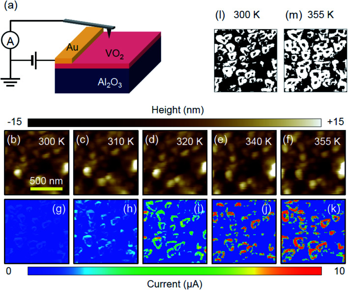
To directly investigate the change in local conductance and the spatial evolution of the M1 and M2 phases during IMT, we performed C-AFM imaging with varying temperatures. An Au electrode was deposited by DC sputtering to measure local currents flowing through the VO2 thin film, as schematically illustrated in Fig. 3(a). In other words, we measured the lateral electronic transport across the film between the tip and the Au electrode, primarily determined by the electrical resistance of VO2 beneath the tip. We note that a similar experimental setup has been used in other C-AFM studies for the IMT of oxide thin films.38 In this experimental geometry, the current value detected at each pixel in the C-AFM images is determined by the sum of a couple of resistances: the tip resistance, the tip–sample contact resistance, the local resistance in the film beneath the tip, and the series resistance across the film between the tip and an electrode. Among them, it is known that the dominant resistances are the tip–sample contact resistance and the local resistance in the film below the tip, i.e., the electrical resistance of the material beneath the tip.38Fig. 3(b)–(f) and (g)–(k) show topography images and simultaneously obtained conductance maps at various temperatures from 300 K to 355 K. For the mapping of local conductances, we applied a small electric bias of +1 V to the Au electrode to avoid unwanted artifacts, such as local Joule heating and electron injection. The topography images show that the applied electric bias and heat did not induce any significant topographic changes during the measurement. We also observed that our VO2 film is granular, presumably due to the aforementioned intrinsic in-plane angle mismatch. The average grain size is approximately 150 nm.
Fig. 3. (a) Schematic diagram of the C-AFM setup. Simultaneously obtained (b)–(f) topography images and (g)–(k) conductance maps with increasing temperature. All images were measured in the same sample area. The scan size was 1 × 1 μm2. (l) and (m) The binary black-and-white images are reconstructed from (g) and (k), respectively. The black and white regions indicate non-conductive regions with noisy currents and conductive regions, respectively.
We observed the donut patterns in the conductance maps at all measured temperatures, as shown in Fig. 3(g)–(k). Based on the Raman spectroscopy results and the previous report,18 we can conclude that the conductive grain boundary and the insulating grain core in a single grain correspond to the M1 and M2 phases, respectively. It is known that grain boundaries exert tensile stress due to intergrain attraction.39,40 Additionally, compressive stress is dominant in the grain core region.18 We note that the M2 phase can be stabilized by applying compressive stress along the direction perpendicular to [011]M1 in granular films.20,41 Therefore, the spatial distribution of M1 and M2 phases is attributed to the difference in local strain states. It is worth noting that the donut patterns in the conductance maps in our VO2 thin film (i.e., the coexistence of M1 and M2 phases) were observed in wide temperature ranges from 300 K to 355 K, which is consistent with the temperature-dependent Raman spectroscopy data. However, in VO2 film on Si substrate,18 the donut patterns were observed in only narrow temperature ranges from 320 K to 335 K. This suggests that the epitaxial stress induced by the c-A12O3 substrate can significantly change the formation and evolution of the intermediate M2 phase.
The current values of conductive grain boundary regions increase with increasing temperature. It should be noted that the maximum value of the measured current is limited by the chosen gain value of the current amplifier. We fixed the gain value to capture tiny current at low temperatures, such as 300 K and 310 K, during the measurement for Fig. 3(g)–(k). By using different gain values depending on temperature, we confirmed that the maximum current value rises by two orders of magnitude at 355 K (∼320 μA) compared to that at 300 K (∼1.3 μA), which agrees with the macroscopic transport data presented in Fig. 2(a). Fig. 3(l) and (m) show the binary black-and-white images reconstructed from Fig. 3(g) and (k), respectively. The black regions indicate non-conductive regions with noisy currents (<100 pA) while the white regions correspond to conductive regions. It can be seen that the conductive regions spread with increasing temperature, indicating the occurrence of intra-grain percolation. The existence of M2 phase and intra-grain percolation process are a fingerprint for Mott transition of VO2,18 which is consistent with the macroscopic IMT and SPT behaviors, i.e., the difference between IMT and SPT temperatures. Note that we also performed the C-AFM measurements under the nitrogen gas environment to test the effect of adsorbates, such as water, and observed similar donut patterns and their temperature-dependent evolution without any noticeable differences [ESI Fig. S1†].
3.4. I–V spectroscopy results and deep data analysis
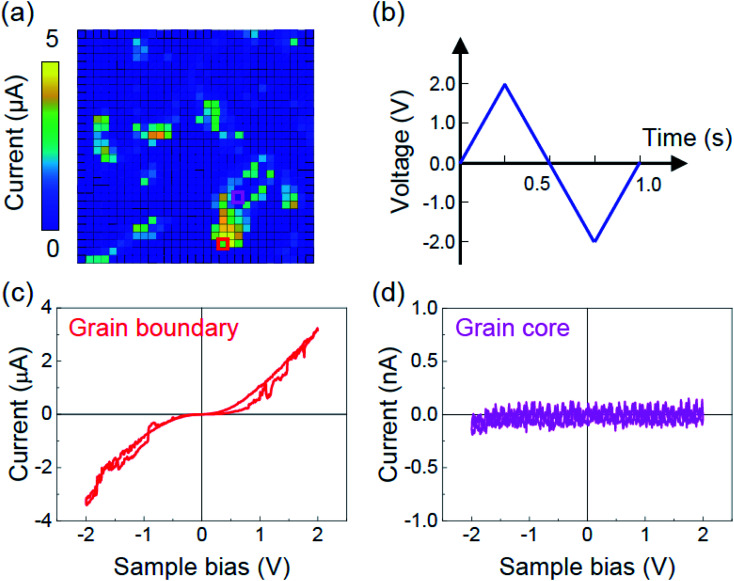
We performed the I–V spectroscopy at room temperature on 30 × 30 points over a 500 × 500 nm2 region to investigate the local conduction behaviors depending on the VO2 phases (i.e., M1 and M2 phases) [Fig. 4(a)]. A bipolar triangular bias waveform (±2 V amplitude, 1 Hz frequency) illustrated in Fig. 4(b) was applied to the Au electrode for the I–V spectroscopy measurement. We observed distinct I–V curves depending on the position inside a single grain [Fig. 4(c) and (d)]. The grain boundary regions (corresponding to the M1 phase) show nonlinear and high current responses [Fig. 4(c)], while the grain core regions (i.e., M2 phase) display negligible noise current responses [Fig. 4(d)].
Fig. 4. (a) Spatial map of the maximum positive current measured by the I–V spectroscopy over the 30 × 30 points. The map size is 500 × 500 nm2. (b) The bias waveform used for the I–V spectroscopy with a frequency of 1 Hz and an amplitude of ±2 V. The I–V curves at (c) the grain boundary and (d) grain core regions marked by open squares in (a).
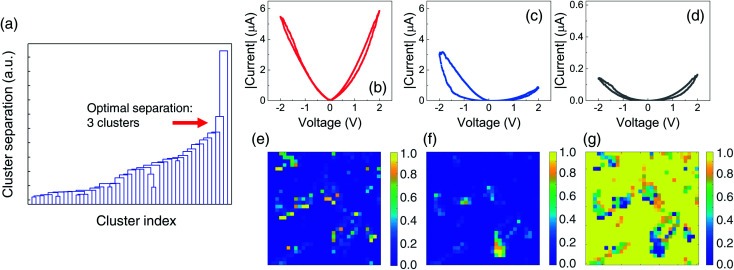
Thereafter, we applied deep data analysis to the multi-dimensional I–V data set collected at 900 points. First, we used the k-means clustering to find the smallest statistically reasonable number of I–V behaviors presented in our epitaxial VO2 thin film system. The k-means clustering allows partitioning n points into k number of clusters having similar behavior using a distance-based algorithm.29,31 It minimizes the sum over all clusters of the within-cluster sum of squared point-to-cluster-mean distances (i.e., variance) as follows:
 |
1 |
where xj is a point in a cluster Si and μi is the mean of points in Si.31 We obtained the dendrogram plot using the k-mean clustering, showing the quality of the cluster separation as a function of the number of clusters, as illustrated in Fig. 5(a). All points in the dendrogram plot are initially classified into a single cluster and are continuously separated down the hierarchy. A larger vertical drop in each of the binary branches indicates a better cluster classification. We found three optimally separated clusters in our I–V data set, as indicated by the red arrow in Fig. 5(a).
Fig. 5. (a) Dendrogram plot of hierarchical binary cluster trees obtained from k-means clustering. Three Bayesian endmembers, i.e., (b) m1, (c) m2, and (d) m3, and corresponding Bayesian loading maps, which show the distribution of abundance coefficients, i.e., (e) α1, (f) α2, and (g) α3.
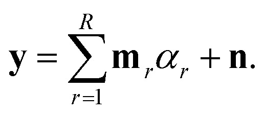
We statistically analyzed the I–V data set using Bayesian linear unmixing.30,31 In the Bayesian approach,30 the data y (in a vector form) is assumed to be a linear combination of location-independent Bayesian endmembers mr with relative fractional abundance coefficient αr, corrupted by additive Gaussian noise n:
 |
2 |
The abundance coefficients satisfy non-negativity and sum-to-one constraints due to physical considerations.30,31Fig. 5(b)–(g) show three Bayesian endmembers and corresponding three Bayesian loading maps extracted from our I–V data set. Endmembers R = 3 were used based on the k-means clustering. The first Bayesian endmember is symmetric in terms of voltage polarity and shows high current behavior. It manifests mostly in the grain boundary regions, corresponding to the M1 phase regions [Fig. 5(b) and (e)]. The second endmember is also observed in the regions of M1 phase [Fig. 5(f)]. However, the current behavior is asymmetric and shows a large I–V loop opening in the negative voltage region [Fig. 5(c)]. Its current value is relatively smaller than that of the first endmember. The third endmember highlights the grain cores, i.e., the M2 phase, and the void regions between grains [Fig. 5(g)]. It has a significantly low and symmetric current response [Fig. 5(d)]. As noted in eqn (2), the conduction behavior at each point in our VO2 film can be represented as a superposition of the three endmembers with corresponding abundance coefficients. Additionally, we stress that the k-means clustering and Bayesian linear unmixing extracted three distinct types of conduction behavior in our VO2 film, which classical C-AFM never resolve. In other words, the classical C-AFM provided only two different conduction behavior between grain cores and boundaries. However, from deep data analysis, we were able to classify the M1 region more.
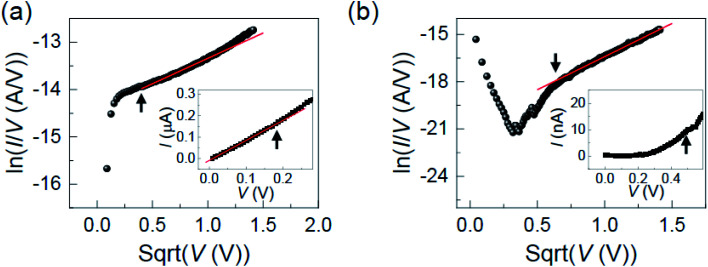
We further investigated the conduction behaviors of the Bayesian endmembers. We only focused on the first and second Bayesian endmembers extracted from the relatively conductive M1 phase regions because the third endmember originated from the highly insulating M2 phase and void regions. It has been reported that the conduction in VO2 films at far below TIMT is dominated by Poole–Frenkel (PF) mechanism,42,43 which is a bulk-limited conduction model to describe trap-assisted electron transport in an electrical insulator. Fig. 6(a) shows the plot of ln(I/V) versus for the forward I–V curve in the positive voltage region of the first Bayesian endmember. The PF mechanism explains well the conduction in the insulating M1 phase regions of our epitaxial VO2 thin film, as indicated by the linear solid red line. The inset in Fig. 6(a) shows the ohmic mode for the very small voltage region (<0.2 V), consistent with other literature.43 The other three I–V curves are also explained by the PF mechanism [ESI Fig. S2†]. The conduction of the second endmember can also be explained by the PF mechanism, as shown in Fig. 6(b) and S3.† However, we note that further investigation, including temperature-dependent I–V spectroscopy, is highly required for a more precise analysis of the conduction mechanism. Finally, we speculate that the voltage polarity-dependent asymmetric conduction behavior observed in the second Bayesian endmember is attributed to the local distribution of charged defects, such as oxygen vacancies.17 Specifically, the oxygen nonstoichiometric region can show an asymmetric I–V curve with a loop opening. In addition, the difference in local strain gradient and consequent flexoelectric field may cause the asymmetry of the I–V curve.44
Fig. 6. The plots of ln(I/V) versus for the forward I–V curve in the positive voltage region of (a) the first and (b) the second Bayesian endmembers. The insets in (a) and (b) show the current responses for the small voltage regions. The solid red lines in (a) and (b) show the linear fitting results. The arrows in (a) and (b) indicate the same voltage values.
4. Conclusions
In summary, we investigated temperature-dependent nanoscale conduction and IMT behavior in an epitaxial VO2 thin film grown on a c-Al2O3 substrate using C-AFM. We observed intriguing donut patterns inside a single grain in C-AFM images, indicating that the grain boundaries are relatively conductive but the grain cores are insulating. The temperature-dependent Raman spectroscopy showed that the observed donut patterns are due to the coexistence of relatively conductive M1 and highly insulating M2 phases. The M1 phase regions spread with increasing temperature, indicating intra-grain percolation. Particularly, we observed the coexistence of M1 and M2 phases in the whole measured temperature range (300–355 K), suggesting that the epitaxial strain plays an important role in the formation and evolution of the intermediate M2 phase. In addition, the existence of M2 phase and intra-grain percolation process indicates our VO2 film undergoes a Mott-type IMT. We further investigated the local conduction mechanism in relatively conductive M1 phase regions using I–V spectroscopy and deep data analysis. The k-means clustering and Bayesian linear unmixing showed the conduction in VO2 film can be classified into three different conduction behaviors. We also found that the conduction behavior in the relatively conductive M1 region can be explained by PF mechanism. This work provides direct nanoscale insight into IMT behavior in the epitaxial VO2 film, especially the coexistence and evolution of M1 and M2 phases. In addition, we highlight that the methodology used in this work, i.e., the I–V spectroscopy combined with deep data analysis, is very powerful in investigating local transport in complex oxides and various material systems.
Conflicts of interest
There are no conflicts to declare.
Supplementary Material
Acknowledgments
This work was supported by the National Research Foundation of Korea (NRF) grant funded by the Korean Government (MSIP) (No. NRF-2019R1A2C1085812). J.-G. Y. acknowledges the support by the National Research Foundation of Korea (NRF) grant funded by the Korean Government (MSIP) (No. NRF-2016R1D1A1B03931721).
Electronic supplementary information (ESI) available. See https://doi.org/10.1039/d2ra02803d
References
- Morin F. J. Oxides which show a metal-to-insulator transition at the neel temperature. Phys. Rev. Lett. 1959;3:34–36. doi: 10.1103/PhysRevLett.3.34. [DOI] [Google Scholar]
- Liu K. Lee S. Yang S. Delaire O. Wu J. Recent progresses on physics and applications of vanadium dioxide. Mater. Today. 2018;21:875–896. doi: 10.1016/j.mattod.2018.03.029. [DOI] [Google Scholar]
- Yang Z. Ko C. Ramanathan S. Oxide electronics utilizing ultrafast metal-insulator transitions. Annu. Rev. Mater. Res. 2011;41:337–367. doi: 10.1146/annurev-matsci-062910-100347. [DOI] [Google Scholar]
- Zhou J. Gao Y. Zhang Z. Luo H. Cao C. Chen Z. Dai L. Liu X. VO2 thermochromic smart window for energy savings and generation. Sci. Rep. 2013;3:3029. doi: 10.1038/srep03029. [DOI] [PMC free article] [PubMed] [Google Scholar]
- Shao Z. Cao X. Luo H. Jin P. Recent progress in the phase-transition mechanism and modulation of vanadium dioxide materials. NPG Asia Mater. 2018;10:581–605. doi: 10.1038/s41427-018-0061-2. [DOI] [Google Scholar]
- Rice T. M. Launois H. Pouget J. P. Comment on “VO2: Peierls or Mott-Hubbard? A view from band theory”. Phys. Rev. Lett. 1994;73:3042. doi: 10.1103/PhysRevLett.73.3042. [DOI] [PubMed] [Google Scholar]
- Kim H.-T. Lee Y. W. Kim B.-J. Chae B.-G. Yun S. J. Kang K.-Y. Han K.-J. Yee K.-J. Lim Y.-S. Monoclinic and correlated metal phase in VO2 as evidence of the Mott transition: coherent phonon analysis. Phys. Rev. Lett. 2006;97:266401. doi: 10.1103/PhysRevLett.97.266401. [DOI] [PubMed] [Google Scholar]
- Wentzcovitch R. M. Schulz W. W. Allen P. B. VO2: Peierls or Mott-Hubbard? A view from band theory. Phys. Rev. Lett. 1994;72:3389–3392. doi: 10.1103/PhysRevLett.72.3389. [DOI] [PubMed] [Google Scholar]
- Cavalleri A. Tóth C. Siders C. W. Squier J. A. Ráksi F. Forget P. Kieffer J. C. Femtosecond structural dynamics in VO2 during an ultrafast solid-solid phase transition. Phys. Rev. Lett. 2001;87:237401. doi: 10.1103/PhysRevLett.87.237401. [DOI] [PubMed] [Google Scholar]
- Weber C. O'Regan D. D. Hine N. D. M. Payne M. C. Kotliar G. Littlewood P. B. Vanadium dioxide: a Peierls-Mott insulator stable against disorder. Phys. Rev. Lett. 2012;108:256402. doi: 10.1103/PhysRevLett.108.256402. [DOI] [PubMed] [Google Scholar]
- Biermann S. Poteryaev A. Lichtenstein A. I. Georges A. Dynamical singlets and correlation-assisted Peierls transition in VO2. Phys. Rev. Lett. 2005;94:026404. doi: 10.1103/PhysRevLett.94.026404. [DOI] [PubMed] [Google Scholar]
- Qazilbash M. M. Brehm M. Chae B.-G. Ho P.-C. Andreev G. O. Kim B.-J. Yun S. J. Balatsky A. V. Maple M. B. Keilmann F. Kim H.-T. Basov D. N. Mott transition in VO2 revealed by infrared spectroscopy and nano-imaging. Science. 2007;318:1750–1753. doi: 10.1126/science.1150124. [DOI] [PubMed] [Google Scholar]
- Frenzel A. Qazilbash M. M. Brehm M. Chae B.-G. Kim B.-J. Kim H.-T. Balatsky A. V. Keilmann F. Basov D. N. Inhomogeneous electronic state near the insulator-to-metal transition in the correlated oxide VO2. Phys. Rev. B: Condens. Matter Mater. Phys. 2009;80:115115. doi: 10.1103/PhysRevB.80.115115. [DOI] [Google Scholar]
- Qazilbash M. M. Tripathi A. Schafgans A. A. Kim B.-J. Kim H.-T. Cai Z. Holt M. V. Maser J. M. Keilmann F. Shpyrko O. G. Basov D. N. Nanoscale imaging of the electronic and structural transitions in vanadium dioxide. Phys. Rev. B: Condens. Matter Mater. Phys. 2011;83:165108. doi: 10.1103/PhysRevB.83.165108. [DOI] [Google Scholar]
- Sohn A. Kanki T. Sakai K. Tanaka H. Kim D.-W. Fractal nature of metallic and insulating domain configurations in a VO2 thin film revealed by Kelvin probe force microscopy. Sci. Rep. 2015;5:10417. doi: 10.1038/srep10417. [DOI] [PMC free article] [PubMed] [Google Scholar]
- Sohn A. Kim H. Kim D.-W. Ko C. Ramanathan S. Park J. Seo G. Kim B.-J. Shin J.-H. Kim H.-T. Evolution of local work function in epitaxial VO2 thin films spanning the metal-insulator transition. Appl. Phys. Lett. 2012;101:191605. doi: 10.1063/1.4766292. [DOI] [Google Scholar]
- Sharma Y. Balachandran J. Sohn C. Krogel J. T. Ganesh P. Collins L. Ievlev A. V. Li Q. Gao X. Balke N. Ovchinnikova O. S. Kalinin S. V. Heinonen O. Lee H. N. Nanoscale control of oxygen defects and metal–insulator transition in epitaxial vanadium dioxides. ACS Nano. 2018;12:7159–7166. doi: 10.1021/acsnano.8b03031. [DOI] [PubMed] [Google Scholar]
- Kim H. Slusar T. V. Wulferding D. Yang I. Cho J.-C. Lee M. Choi H. C. Jeong Y. H. Kim H.-T. Kim J. Direct observation of the M2 phase with its Mott transition in a VO2 film. Appl. Phys. Lett. 2016;109:233104. doi: 10.1063/1.4971848. [DOI] [Google Scholar]
- Kim J. Ko C. Frenzel A. Ramanathan S. Hoffman J. E. Nanoscale imaging and control of resistance switching in VO2 at room temperature. Appl. Phys. Lett. 2010;96:213106. doi: 10.1063/1.3435466. [DOI] [Google Scholar]
- Ji Y. Zhang Y. Gao M. Yuan Z. Xia Y. Jin C. Tao B. Chen C. Jia Q. Lin Y. Role of microstructures on the M1-M2 phase transition in epitaxial VO2 thin films. Sci. Rep. 2014;4:4854. doi: 10.1038/srep04854. [DOI] [PMC free article] [PubMed] [Google Scholar]
- Atkin J. M. Berweger S. Chavez E. K. Raschke M. B. Cao J. Fan W. Wu J. Strain and temperature dependence of the insulating phases of VO2 near the metal-insulator transition. Phys. Rev. B: Condens. Matter Mater. Phys. 2012;85:020101. doi: 10.1103/PhysRevB.85.020101. [DOI] [Google Scholar]
- Cao J. Gu Y. Fan W. Chen L. Q. Ogletree D. F. Chen K. Tamura N. Kunz M. Barrett C. Seidel J. Wu J. Extended mapping and exploration of the vanadium dioxide stress-temperature phase diagram. Nano Lett. 2010;10:2667–2673. doi: 10.1021/nl101457k. [DOI] [PubMed] [Google Scholar]
- Okimura K. Sakai J. Ramanathan S. In situ X-ray diffraction studies on epitaxial VO2 films grown on c-Al2O3 during thermally induced insulator-metal transition. J. Appl. Phys. 2010;107:063503. doi: 10.1063/1.3327422. [DOI] [Google Scholar]
- Park J. H. Coy J. M. Kasirga T. S. Huang C. Fei Z. Hunter S. Cobden D. H. Measurement of a solid-state triple point at the metal–insulator transition in VO2. Nature. 2013;500:431–434. doi: 10.1038/nature12425. [DOI] [PubMed] [Google Scholar]
- Marezio M. McWhan D. B. Remeika J. P. Dernier P. D. Structural aspects of the metal-insulator transitions in Cr-doped VO2. Phys. Rev. B: Solid State. 1972;5:2541–2551. doi: 10.1103/PhysRevB.5.2541. [DOI] [Google Scholar]
- Pouget J. P. Launois H. Rice T. M. Dernier P. Gossard A. Villeneuve G. Hagenmuller P. Dimerization of a linear Heisenberg chain in the insulating phases of V1-xCrxO2. Phys. Rev. B: Solid State. 1974;10:1801–1815. doi: 10.1103/PhysRevB.10.1801. [DOI] [Google Scholar]
- Yang S. M. Paranthaman M. P. Noh T. W. Kalinin S. V. Strelcov E. Nanoparticle shape evolution and proximity effects during tip-induced electrochemical processes. ACS Nano. 2016;10:663–671. doi: 10.1021/acsnano.5b05686. [DOI] [PubMed] [Google Scholar]
- Yang S. M. Lee S. Jian J. Zhang W. Lu P. Jia Q. Wang H. Won Noh T. Kalinin S. V. MacManus-Driscoll J. L. Strongly enhanced oxygen ion transport through samarium-doped CeO2 nanopillars in nanocomposite films. Nat. Commun. 2015;6:8588. doi: 10.1038/ncomms9588. [DOI] [PMC free article] [PubMed] [Google Scholar]
- Hartigan J. A. Wong M. A. A k-means clustering algorithm. J. R. Stat. Soc., C: Appl. Stat. 1979;28:100–108. [Google Scholar]
- Dobigeon N. Moussaoui S. Coulon M. Tourneret J. Hero A. O. Joint Bayesian endmember extraction and linear unmixing for hyperspectral imagery. IEEE Trans. Signal Process. 2009;57:4355–4368. [Google Scholar]
- Strelcov E. Belianinov A. Hsieh Y.-H. Jesse S. Baddorf A. P. Chu Y.-H. Kalinin S. V. Deep data analysis of conductive phenomena on complex oxide interfaces: physics from data mining. ACS Nano. 2014;8:6449–6457. doi: 10.1021/nn502029b. [DOI] [PubMed] [Google Scholar]
- Belianinov A. Vasudevan R. Strelcov E. Steed C. Yang S. Tselev A. Jesse S. Biegalski M. Shipman G. Symons C. Borisevich A. Archibald R. Kalinin S. Big data and deep data in scanning and electron microscopies: deriving functionality from multidimensional data sets. Adv. Struct. Chem. Imaging. 2015;1:6. doi: 10.1186/s40679-015-0006-6. [DOI] [PMC free article] [PubMed] [Google Scholar]
- Yoon J.-G. A new approach to the fabrication of memristive neuromorphic devices: compositionally graded films. Materials. 2020;13:3680. doi: 10.3390/ma13173680. [DOI] [PMC free article] [PubMed] [Google Scholar]
- Yang M. Yang Y. Hong B. Huang H. Hu S. Dong Y. Wang H. He H. Zhao J. Liu X. Luo Z. Li X. Zhang H. Gao C. Resistance switching of epitaxial VO2/Al2O3 heterostructure at room temperature induced by organic liquids. AIP Adv. 2015;5:037114. doi: 10.1063/1.4914915. [DOI] [Google Scholar]
- Hong B. Hu K. Tao Z. Zhao J. Pan N. Wang X. Lu M. Yang Y. Luo Z. Gao C. Polymorph separation induced by angle distortion and electron delocalization effect via orbital modification in VO2 epitaxial thin films. Phys. Rev. B. 2017;95:075433. doi: 10.1103/PhysRevB.95.075433. [DOI] [Google Scholar]
- Park J. Yoon H. Sim H. Choi S.-Y. Son J. Accelerated hydrogen diffusion and surface exchange by domain boundaries in epitaxial VO2 thin films. ACS Nano. 2020;14:2533–2541. doi: 10.1021/acsnano.0c00441. [DOI] [PubMed] [Google Scholar]
- Choi Y. Lee D. Song S. Kim J. Ju T.-S. Kim H. Kim J. Yoon S. Kim Y. Phan T. B. Bae J.-S. Park S. Correlation between symmetry and phase transition temperature of VO2 films deposited on Al2O3 substrates with various orientations. Adv. Electron. Mater. 2021;7:2000874. doi: 10.1002/aelm.202000874. [DOI] [Google Scholar]
- Preziosi D. Lopez-Mir L. Li X. Cornelissen T. Lee J. H. Trier F. Bouzehouane K. Valencia S. Gloter A. Barthélémy A. Bibes M. Direct mapping of phase separation across the metal–insulator transition of NdNiO3. Nano Lett. 2018;18:2226–2232. doi: 10.1021/acs.nanolett.7b04728. [DOI] [PubMed] [Google Scholar]
- Doljack F. A. Hoffman R. W. The origins of stress in thin nickel films. Thin Solid Films. 1972;12:71–74. doi: 10.1016/0040-6090(72)90396-3. [DOI] [Google Scholar]
- Janssen G. C. A. M. Dammers A. J. Sivel V. G. M. Wang W. R. Tensile stress in hard metal films. Appl. Phys. Lett. 2003;83:3287–3289. doi: 10.1063/1.1619561. [DOI] [Google Scholar]
- Okimura K. Watanabe T. Sakai J. Stress-induced VO2 films with M2 monoclinic phase stable at room temperature grown by inductively coupled plasma-assisted reactive sputtering. J. Appl. Phys. 2012;111:073514. doi: 10.1063/1.3700210. [DOI] [Google Scholar]
- Yang Z. Ko C. Balakrishnan V. Gopalakrishnan G. Ramanathan S. Dielectric and carrier transport properties of vanadium dioxide thin films across the phase transition utilizing gated capacitor devices. Phys. Rev. B: Condens. Matter Mater. Phys. 2010;82:205101. doi: 10.1103/PhysRevB.82.205101. [DOI] [Google Scholar]
- Ko C. Ramanathan S. Observation of electric field-assisted phase transition in thin film vanadium oxide in a metal-oxide-semiconductor device geometry. Appl. Phys. Lett. 2008;93:252101. doi: 10.1063/1.3050464. [DOI] [Google Scholar]
- Park S. M. Wang B. Chen L.-Q. Noh T. W. Yang S. M. Lee D. Flexoelectric control of physical properties by atomic force microscopy. Appl. Phys. Rev. 2021;8:041327. [Google Scholar]
Associated Data
This section collects any data citations, data availability statements, or supplementary materials included in this article.


