Abstract
The effects of the sintering conditions on the phase compositions, microstructure, electrical properties, and dielectric responses of TiO2-excessive Na1/2Y1/2Cu3Ti4.1O12 ceramics prepared by a solid-state reaction method were investigated. A pure phase of the Na1/2Y1/2Cu3Ti4.1O12 ceramic was achieved in all sintered ceramics. The mean grain size slightly increased with increasing sintering time (from 1 to 15 h after sintering at 1070 °C) and sintering temperature from 1070 to 1090 °C for 5 h. The primary elements were dispersed in the microstructure. Low dielectric loss tangents (tan δ~0.018–0.022) were obtained. Moreover, the dielectric constant increased from ε′~5396 to 25,565 upon changing the sintering conditions. The lowest tan δ of 0.009 at 1 kHz was obtained. The electrical responses of the semiconducting grain and insulating grain boundary were studied using impedance and admittance spectroscopies. The breakdown voltage and nonlinear coefficient decreased significantly as the sintering temperature and time increased. The presence of Cu+, Cu3+, and Ti3+ was examined using X-ray photoelectron spectroscopy, confirming the formation of semiconducting grains. The dielectric and electrical properties were described using Maxwell–Wagner relaxation, based on the internal barrier layer capacitor model.
Keywords: giant/colossal dielectric permittivity, varistor, admittance spectroscopy, impedance spectroscopy, Maxwell–Wagner polarization
1. Introduction
Dielectric materials are among the most interesting materials for use in electronic devices such as capacitors and high-energy storage devices [1,2]. CaCu3Ti4O12 (CCTO) has been extensively studied because CCTO can exhibit a high dielectric constant (ε′ > 104) [3,4,5,6,7,8]. Furthermore, CCTO ceramic is not a ferroelectric material. The observed large ε′ value was stable with respect to temperature and frequency. However, the dielectric loss tangent remains too high (tan δ > 0.1) and cannot be applied to electronic devices. Many years ago, researchers attempted to improve the dielectric properties of CCTO by increasing ε′, reducing tan δ, and increasing the efficiency of dielectric properties for stability with temperature and frequency [6,7,9,10]. It is believed that the origin of the dielectric properties of CCTO arises from its microstructure, consisting of an insulating grain boundary (i-GBs) and a semiconducting grain (semi-G). This microstructure is called an internal barrier layer capacitor (IBLC) structure [3,11].
In the IBLC model, tan δ can be reduced by increasing the grain boundary resistance (Rgb) [12,13]. In 2006, Y. Lin et al. reduced the tan δ in CCTO from 0.07 to 0.03 by adding composite TiO2 into samples [9]. When the Rgb was analyzed using impedance spectroscopy, it appeared that Rgb increased with increasing TiO2 contents in CCTO ceramics. Moreover, the breakdown electric field (Eb) of the nonlinear J-E characteristics increased with increasing TiO2 contents, indicating that Rgb can be increased by adding TiO2 to CCTO ceramics, resulting in a decrease in tan δ, which corresponds to the IBCL model [9,14].
The optimized sintering condition is one technique that has been used to improve dielectric properties, which can modify the microstructure of ceramics. The effect of sintering temperature results in grain size changes and i-GBs. Generally, ε′ can be increased by increasing the temperature and duration of sintering in ACu3Ti4O12 ceramics [11,15,16,17].
ACu3Ti4O12 is a dielectric material group that has received extensive attention because of its interesting dielectric properties. CaCu3Ti4O12 (CCTO) [4,5], CdCu3Ti4O12 (CdCTO) [18,19], Na1/2Sm1/2Cu3Ti4O12 (NSmCTO) [20], Na1/2Y1/2Cu3Ti4O12 (NYCTO) [16,21,22,23], Na1/2La1/2Cu3Ti4O12 (NLCTO) [24,25], Y2/3Cu3Ti4O12 (YCTO) [26,27], La2/3Cu3Ti4O12 (LCTO) [28], Bi2/3Cu3Ti4O12 (BCTO) [29,30,31,32], and Na1/2Bi1/2Cu3Ti4O12 (NBCTO) [17,33,34] were dielectric materials in the ACu3Ti4O12 oxides group. These materials have perovskite structures and often have reported excellent dielectric properties. However, these materials still have limitations under many conditions for application in electronic devices. The dielectric properties of CCTO and NYCTO ceramics can be significantly improved by the addition of excess TiO2 [9,21].
Most recently, the tan δ value of Na1/2Y1/2Cu3Ti4.1O12 can be significantly reduced (tan δ < 0.1), while the ε′ value is still larger than 104. The improved dielectric properties were attributed to the enhanced electrical properties of the i-GBs due to the excessive TiO2-rich phase boundaries, which are also associated with the oxygen content along the i-GBs. Generally, the giant dielectric properties of CCTO-based materials are closely related to sintering conditions [5,35,36]. Thus, the giant dielectric properties can be optimized by tuning the sintering conditions. It is hypothesized that the dielectric properties of Na1/2Y1/2Cu3Ti4.1O12 can be further improved by varying the sintering conditions. The optimization of fabrication conditions is one of the most important topics for developing materials used in electronic devices. This is the motivation of this work. Hence, the aim of this study was to investigate the effect of sintering conditions on the dielectric properties of Na1/2Y1/2Cu3Ti4.1O12 to optimize the dielectric properties.
In this study, the effects of sintering conditions on the dielectric and electrical properties of Na1/2Y1/2Cu3Ti4.1O12 ceramics were investigated. The phase composition and microstructure were analyzed. Significant improvements in the dielectric and electrical behaviors with respect to ε′ and tan δ were achieved. The origin of the observed dielectric and electrical properties is described.
2. Experimental Details
Na1/2Y1/2Cu3Ti4.1O12 powder was prepared using the solid-state reaction method (SSR). The starting materials were Na2CO3 (Sigma-Aldrich, St. Louis, MO, USA, 99.9%), Y2O3 (CERAC, 99.99%), CuO (Sigma-Aldrich, St. Louis, MO, USA, 99.9%), and TiO2 (Sigma-Aldrich, St. Louis, MO, USA, 99.9%). The powders were mixed using a ball milling method for 24 h. The powder was calcined at 1000 °C in air for 10 h at heating and cooling rates of 5 °C/min. The calcined powder was finely crushed and compressed into pellets for sintering. The first set of pellets was sintered at 1070 °C for 1, 5, and 15 h. The second set of pellets was sintered at 1080 and 1090 °C for 5 h. The samples produced under these conditions are referred to as 1NYCTTiO, 2NYCTTiO, 3NYCTTiO, 4NYCTTiO, and 5NYCTTiO, respectively.
The phase compositions were analyzed by X-ray diffraction (XRD, PANalytical, EMPYREAN). The XRD patterns were measured in the 2θ range of 25–70°, and the lattice parameters were calculated using the Rietveld technique. The surfaces of the ceramics were characterized by scanning electron microscopy (SEM, SEC, SNE-4500 M). The element distributions were analyzed using a mapping technique, and field emission scanning electron microscopy (FIB-FESEM) was used for SEM mapping. X-ray photoemission spectroscopy (XPS, PHI5000 Versarobe II, ULVAC-PHI) was used to analyze the oxidation states of the Na1/2Y1/2Cu3Ti4.1O12 ceramics. The densities of the sintered samples were measured.
To determine the dielectric and electrical properties, the as-sintered ceramics were polished to a smooth surface. Next, parallel-plate electrodes were made by painting Ag paste on both sides of the smooth surfaces. Then, the sample with top and bottom electrodes was heated in air at 600 °C for 30 min. The area of the top and bottom electrodes was 2.83 cm2. The capacitance (Cp) and tan δ were measured in the frequency range of 102 to 106 Hz at room temperature using an impedance analyzer (KEYSIGHT E4990A). The amplitude of the ac field was 0.5 V. In addition, the dielectric behavior was studied in the temperature range of −60 to 210 °C. Finally, the nonlinear electrical (I–V) properties were diagnosed using a high-voltage measurement unit (Keithley 247 model).
The ε′ value was calculated by the equation:
| (1) |
where ε0 is the permittivity of free space and S and t are the electrode area and sample thickness, respectively. The complex dielectric permittivity () was used to calculate the complex impedance (Z*) using Equation (2).
| (2) |
where and are the real part and imaginary part of Z*, respectively, and are the real and imaginary parts of , is the empty cell capacitance, , and ω is the angular frequency (ω = 2πf).
3. Results and Discussion
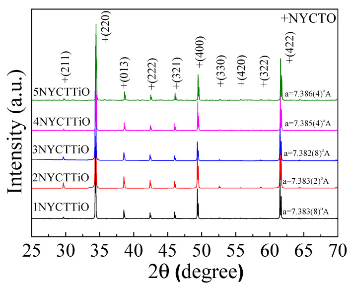
The XRD characteristics of the sintered Na1/2Y1/2Cu3Ti4.1O12 ceramics were analyzed. Accordingly, the lattice parameters were calculated using the Rietveld technique. Figure 1 shows the XRD patterns of all samples, showing the pure phase (not detecting the second phase and not detecting the TiO2 phase) with the perovskite structure (JCPDS 75–2188). The lattice parameters of 1NYCTTiO, 2NYCTTiO, 3NYCTTiO, 4NYCTTiO, and 5NYCTTiO were 7.383(8), 7.383(2), 7.382(8), 7.385(4), and 7.386(4) Å, respectively. The sintering conditions did not affect the lattice parameters of the Na1/2Y1/2Cu3Ti4.1O12 ceramics. Moreover, the XRD patterns and lattice parameters were comparable to the XRD spectra that were reported for Na1/2Y1/2Cu3Ti4O12 (NYCTO) ceramics [16,21,22,23].
Figure 1.
XRD patterns of the Na1/2Y1/2Cu3Ti4.1O12 ceramics sintered at 1070 °C for 1, 5, and 15 h and sintered at 1080 and 1090 °C for 5 h.
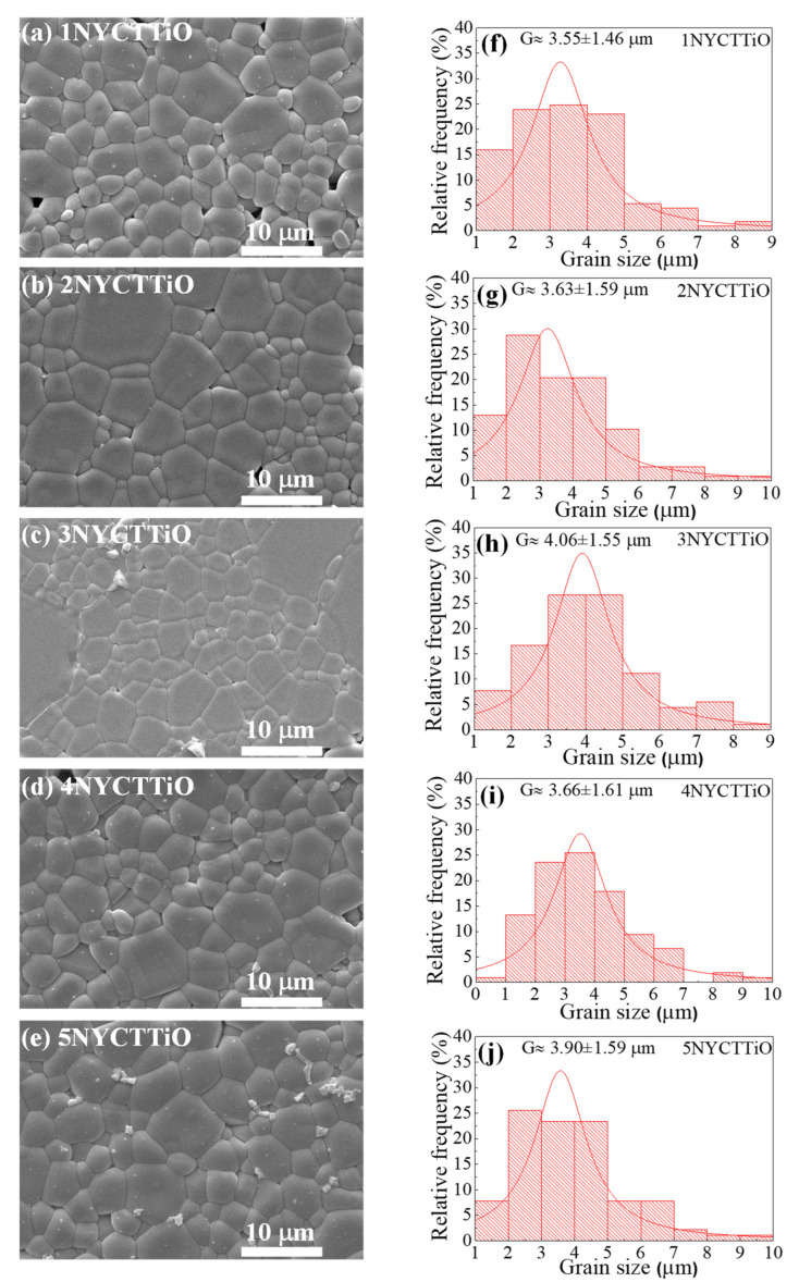
Figure 2a–e show the morphologies of Na1/2Y1/2Cu3Ti4.1O12 ceramics sintered under different conditions using the SEM technique. The SEM images clearly show the grains and GBs. A small number of pores can be observed. The grain-size distributions are shown in Figure 2f–j. The mean grain sizes of the 1NYCTTiO, 2NYCTTiO, 3NYCTTiO, 4NYCTTiO, and 5NYCTTiO samples were 3.55 ± 1.46, 3.63 ± 1.59, 4.06 ± 1.55, 3.66 ± 1.61, and 3.90 ± 1.59 μm, respectively. The average grain size increased slightly with increasing temperature and time in the sintering process, which may have been caused by the enhanced diffusion of ions [6,7]. The densities of the samples were 96.34, 97.40, 97.67, 95.61, and 96.90%, respectively.
Figure 2.
SEM images of polished surfaces of Na1/2Y1/2Cu3Ti4.1O12 ceramics sintered at (a) 1070 °C for 1 h, (b) 1070 °C for 5 h, (c) 1070 °C for 15 h, (d) 1080 °C for 5 h, and (e) 1090 °C for 5 h and grain size distributions with sintering at (f) 1070 °C for 1 h, (g) 1070 °C for 5 h, (h) 1070 °C for 15 h, (i) 1080 °C for 5 h, and (j) 1090 °C for 5 h.
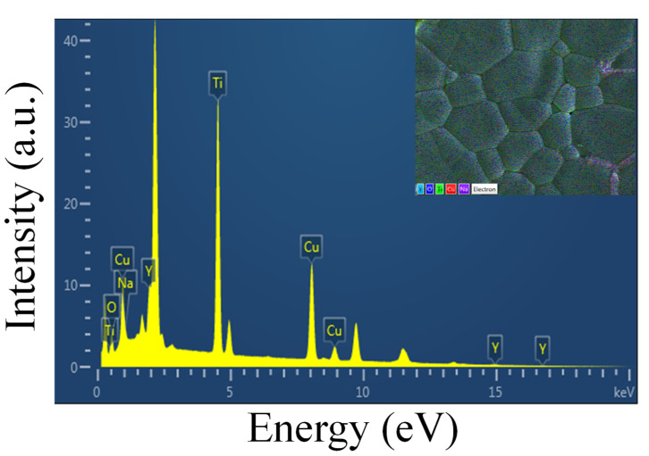
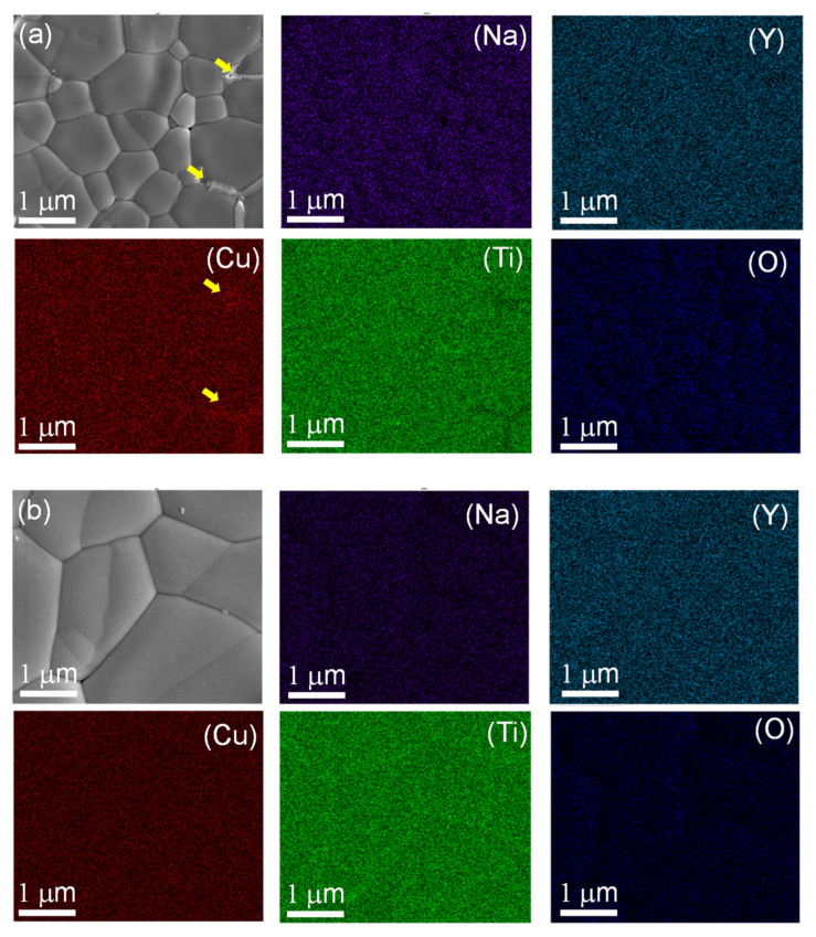
The elemental composition of the Na1/2Y1/2Cu3Ti4.1O12 ceramic sintered at 1070 °C for 15 h was studied using EDS. The EDS spectrum shown in Figure 3 can be used to observe the major elements consisting of Na, Y, Cu, Ti, and O peaks to confirm the elemental composition of the ceramics. The mapping technique was used to study the elemental distribution, as shown in Figure 4a,b. All elements were homogeneously dispersed inside the grains. Figure 4a shows the distribution of elements; all elements were well-distributed throughout the sample. However, segregation of Cu was observed around the GB to detect CuO, which may have been caused by the effect of sintering temperature and increasing Ti concentration. The concentration of excess Ti may enter into the Cu sites in the structure, causing the segregation of CuO at the GB during the temperature sintering process [9,10,11]. Moreover, when examining the distribution of elements at the GB in the area without CuO, Ti element was detected at the GB, indicating that excess Ti tends to unite at the GB, as shown in Figure 4b. Generally, TiO2 and CuO have electrical insulating properties; detecting this at the GB may result in an increase in resistance at the GB, which is an important factor for reducing tan δ in perovskite dielectric materials [10].
Figure 3.
EDS spectrum of Na1/2Y1/2Cu3Ti4.1O12 ceramic sintered at 1070 °C for 15 h.
Figure 4.
SEM mapping images of Na, Y, Cu, Ti, and O considering the amount of Cu (a) and Ti (b) at the grain boundary of the Na1/2Y1/2Cu3Ti4.1O12 ceramic sintered at 1070 °C for 15 h.
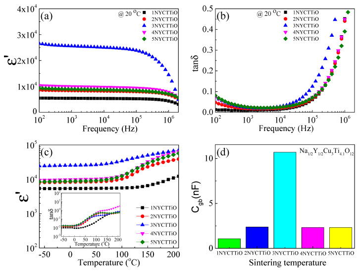
Depending on the frequency shown in Figure 5a, the ε′ values at 1 kHz and 20 °C for the 1NYCTTiO, 2NYCTTiO, 3NYCTTiO, 4NYCTTiO, and 5NYCTTiO samples were 5396, 8370, 25,565, 9972, and 8896, respectively. The ε′ values tended to increase with increasing sintering duration and slightly increased with increasing sintering temperature, which might be a result of the increasing grain size when this result was considered using the IBLC model [6,15,16,17,18]. It was also observed that ε′ was a relatively stable frequency. However, at a high frequency (>105 Hz), ε′ rapidly dropped because of the dielectric relaxation process. Moreover, all the samples had a low tan δ (<0.05) over the frequency range of 70–100 kHz. tan δ slightly changed with increasing sintering duration and sintering temperature. The tan δ values of the samples were 0.009, 0.018, 0.022, 0.024, and 0.025, respectively, as observed in Figure 5b. However, tan δ increased rapidly at frequencies higher than 105 Hz. This is the dielectric relaxation response, which is related to the fast ε′ drop at high frequencies. These behaviors are similar to the dielectric behaviors that occur in CCTO and NYCTO ceramics [1,2,3,4,5,6,7,8]. The dielectric relaxation at high frequencies was caused by the fact that the electric dipole cannot complete the polarization process because the relaxation time is too small.
Figure 5.
(a) Dielectric constant (ε′) and (b) dielectric loss tangent (tan δ) at room temperature (20 °C) as a function of frequency for Na1/2Y1/2Cu3Ti4.1O12 ceramics sintered under different conditions. (c) Dielectric constant (ε′) and (inset) dielectric loss tangent (tan δ) as a function of temperature in the range of −60 to 210 °C. (d) Grain-boundary capacitance (Cgb).
Figure 5c shows the dependence of ε′ and tan δ on the temperature. The ε′ and tan δ values of the 2NYCTTiO, 4NYCTTiO, and 5NYCTTiO samples were greatly increased when the temperature was above 90 °C. These dielectric responses were caused by the electric charge having high energy (maybe more than the potential energy at the GB) and being easier to move at a high temperature. As a result, the polarization process occurs more easily and the electrical conductivity increases [19,20,21,22]. However, the ε′ values of the 1NYCTTiO and 3NYCTTiO samples were relatively stable with temperature, indicating that the sintering condition for ε′ stability with temperature was successfully achieved. As shown in Figure 5d, the GB capacitance (Cgb) values were calculated in the temperature range of 150–200 °C using the electric modulus (M*) technique. The Cgb values of the 1NYCTTiO, 2NYCTTiO, 3NYCTTiO, 4NYCTTiO, 5NYCTTiO samples were 1.07, 2.38, 10.7, 2.32, and 2.32 nF, respectively. The Cgb values did not change with increasing sintering temperatures due to the small change in the sintering temperature. However, Cgb tended to increase with increasing sintering duration, which corresponds to an increase in ε′. This may be the major factor causing the ε′ rise when using the IBLC model [6]. In this study, excellent dielectric properties were obtained for the 3NYCTTiO samples.
The excellent dielectric properties of NYCTO are attributed to the electrically the heterogeneous microstructure of the materials. These microstructures consist of i-GBs (high resistance) and semi-Gs (low resistance). The electrical circuit model explained the electrical conductivity of the materials, which consisted of a capacitor (C) and a resistor (R) connected in series (RC circuits). Thus, impedance spectroscopy was used to analyze the electrical properties of the ceramic materials. Normally, the grain resistance (Rg) and GB resistance (Rgb) are obtained by the small semicircle (or nonzero intercept) and large semicircle observed from Z* plots, respectively. Moreover, the grain capacitance (Cg) and GB capacitance (Cgb) can be calculated using impedance spectroscopy [2,23]. Z* is calculated using Equation (3).
| (3) |
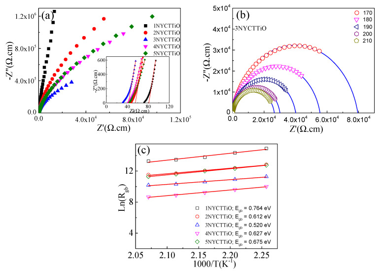
Figure 6a shows the impedance complex plane (Z*) plots of the 1NYCTTiO, 2NYCTTiO, 3NYCTTiO, 4NYCTTiO, and 5NYCTTiO samples. The large semicircle tended to decrease with increasing sintering duration and slightly decreased with increasing sintering temperature, indicating that Rgb tended to decrease with increasing sintering duration and sintering temperature. Moreover, the Rg tended to decrease with increasing sintering duration (Rg was trivially changed with increasing sintering temperature) when observed from the non-zero intercept in the inset of Figure 6a. The effects of changing the Rg and Rgb on the dielectric properties were investigated.
Figure 6.
(a) Impedance complex plane plot at 20 °C and inset non-zero intercept of Na1/2Y1/2Cu3Ti4.1O12 ceramics sintered at 1070 °C for 1, 5, and 15 h and sintered at 1080 and 1090 °C for 5h. (b) Impedance complex plane plot in the temperature range of 170–210 °C for the sample sintered at 1070 °C for 15 h. (c) Arrhenius plot of the grain boundary conductivity (Rgb).
To calculate the activation at the GB (Egb), Rgb was obtained by fitting the Z* data with the IBLC model at various temperatures. For the IBLC structure of CCTO-based ceramics, the microstructure consisted of i-GBs and semi-G [3]. Generally, the Cgb values of the ceramics were much higher than their Cg values (Cgb >> Cg). Therefore, Equation (3) can be modified to create a fitting model as follows [9]:
| (4) |
where α is a constant (). The Rgb values were obtained by fitting the experimental data of Z* in the temperature range of 170–210 °C. Figure 6b shows the fitted results of Z* plots for the 3NYCTTiO sample for calculating the Egb value. The other samples were fitted using the same process (data not shown). Next, the Egb values were calculated using the Arrhenius law:
| (5) |
where kB is the Boltzmann constant, T is the temperature (Kelvins), and R0 is a pre-exponential constant term. As shown in Figure 6c, the Egb values of 1NYCTTiO, 2NYCTTiO, 3NYCTTiO, 4NYCTTiO, and 5NYCTTiO were 0.764, 0.612, 0.520, 0.627, and 0.675 eV, respectively. The Egb values tended to decrease with increasing sintering durations, but the Egb values trivially changed with increasing sintering temperatures, similar to Rgb. The Egb values of all samples were close to those reported for CCTO and NYCTO ceramics (≈0.6 eV), confirming that the GBs of the samples were electrically insulating [1,6,24,25]. Furthermore, the decrease in the Egb values might be caused by an increase in the number of oxygen vacancies.
To study the dielectric properties of Na1/2Y1/2Cu3Ti4.1O12 and other ACu3Ti4O12 compounds, the conductivity of the semi-Gs was considered to be an important factor. Generally, Rg is calculated from the nonzero intercept on the Z’-axis in the Z* plot. The conductivity of the semi-Gs was confirmed by calculating the Eg value (activation energy in the grain). In this study, Eg was calculated using admittance spectroscopy (Y*). According to the IBLC model, for the equivalent circuit (RC), when Rg << Rgb and Cg << Cgb, the electrical conductivity can be analyzed using Equation (6):
| (6) |
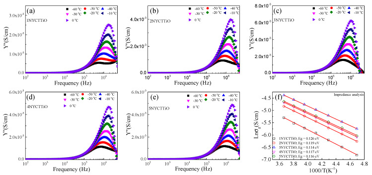
where and . , , and . When using Equation (6), this equation can be reduced to , where is the maximum value at -peak. The values of the 1NYCTTiO, 2NYCTTiO, 3NYCTTiO, 4NYCTTiO, and 5NYCTTiO samples are shown in Figure 7a–e. In addition, the Eg values were calculated using the Arrhenius law:
| (7) |
where Eg is the activation energy for the conductivity in the grain. The Eg values were calculated in the temperature range from −60 to 0 °C, as shown in Figure 7f. The Eg values of 1NYCTTiO, 2NYCTTiO, 3NYCTTiO, 4NYCTTiO, and 5NYCTTiO were 0.126, 0.119, 0.114, 0.117, and 0.116 eV, respectively. The Eg values were close to those reported for NYCTO ceramics, indicating that the grain was a semiconductor [5,6,8,26,27]. Moreover, Eg tends to decrease slightly with increasing sintering duration (Eg is trivially changed with increasing sintering temperatures), and the sintering duration corresponds to a decrease in Rg. The reductions in Eg and Rg correspond to an increase in ε′, which is an important factor for explaining the dielectric properties of Na1/2Y1/2Cu3Ti4.1O12 ceramics. The relationship between the dielectric permittivity and the electrical conductivity of the semi-Gs and i-GBs is presented in Table 1.
Figure 7.
Admittance imaginary (Y″) as a function of the frequency plot in the temperature range of −60–0 °C for Na1/2Y1/2Cu3Ti4.1O12 ceramics sintered at (a) 1070 °C for 1 h, (b) 1070 °C for 5 h, (c) 1070 °C for 15 h, (d) 1080 °C for 5 h, and (e) 1090 °C for 5 h. (f) Arrhenius plot of grain conductivity (σg).
Table 1.
ε′ at 1 kHz and 20 °C, Rg at 20 °C, and calculated Eg, Egb, and Cgb of Na1/2Y1/2Cu3Ti4.1O12 sintered at 1070 °C for 1, 5, and 15 h and sintered at 1080 and 1090 °C for 5 h.
| Sample | Rg (Ω) | Eg (eV) | Egb (eV) | Cgb (nF) | ε’ |
|---|---|---|---|---|---|
| 1NYCTTiO | 83 | 0.126 | 0.764 | 1.07 | 5396 |
| 2NYCTTiO | 54 | 0.119 | 0.612 | 2.38 | 8370 |
| 3NYCTTiO | 41 | 0.114 | 0.520 | 10.7 | 25,565 |
| 4NYCTTiO | 48 | 0.117 | 0.627 | 2.32 | 9972 |
| 5NYCTTiO | 49 | 0.116 | 0.675 | 2.32 | 8896 |
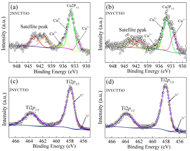
Normally, the grains of ACu3Ti4O12 ceramics are semiconducting. Thus, studying the electrical properties of grains plays an important role in changing the dielectric properties of ceramic materials. The oxidation states of the Ti and Cu ions in the grains were investigated using XPS. Figure 8a–d show the electron hopping between Cu+ Cu2+, Cu2+ Cu3+, and Ti3+ Ti4+ in the 2NYCTTiO and 3NYCTTiO samples. The peaks of Cu2p3/2 were fitted using Gaussian–Lorentzian models, as shown in Figure 8a,b, and the peaks of Cu+, Cu2+, and Cu3+ were observed at the mean binding energies of approximately ≈932.13–932.25, 933.92–934.09, and 935.63–936.10 eV, respectively. The calculated Cu+/Cu2+ of the 2NYCTTiO and 3NYCTTiO samples were 18.34% and 45.62%. The Cu+/Cu2+ ratio tends to increase with increasing sintering durations. Two peaks of Ti 2p3/2 are shown in Figure 8c,d. The Ti3+/Ti4+ ratios were 3.33% and 3.18%, which almost did not change with increasing sintering durations, indicating that the effect of sintering was not affected by electron hopping between Ti3+ Ti4+. Thus, the electrical properties of the grains may result from electron hopping between Cu+ Cu2+. Generally, the electrical conductivity depends on the concentration of free charges and the mobility of the charge carriers in the material. ACu3Ti4O12 ceramics often lose oxygen during sintering, resulting in oxygen vacancies and free electrons [28,29]. Accordingly, increasing the Cu+/Cu2+ ratio indicates an increase in the electrical conductivity of the grains. The increasing electrical conductivity within the grains was related to a decrease in Rg, which may be the major cause of the ε′ increase, which can be described based on the IBLC model [30].
Figure 8.
(a,b) XPS spectra of Cu2p and (c,d) XPS spectra of Ti2p3/2 for Na1/2Y1/2Cu3Ti4.1O12 ceramics sintered at 1070 °C for 5 and 15 h.
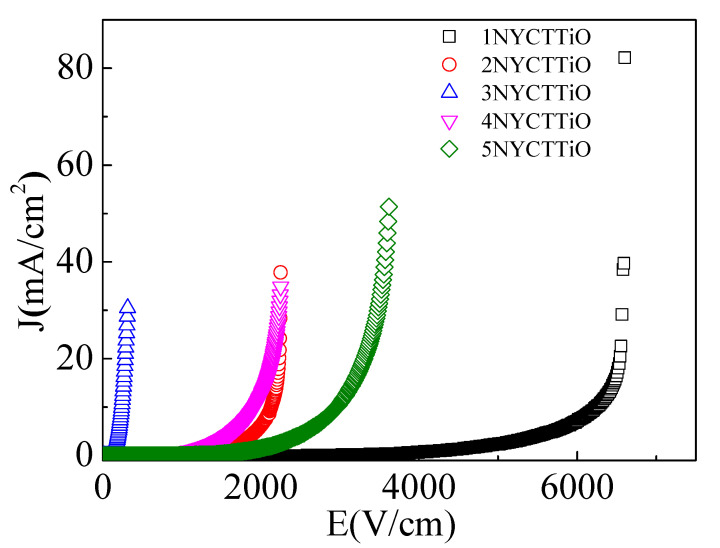
The non-ohmic characteristics of ACu3Ti4O12 ceramics have been extensively studied to explain their electrical behavior in the Rgb of materials. The effect of sintering duration on the nonlinear current density–electric field (J–E) characteristics of the Na1/2Y1/2Cu3Ti4.1O12 ceramics is shown in Figure 9. The Eb and the nonlinear coefficient (α) can be calculated. Both values can be calculated using the equation of varistor characteristics (I = KVα), where K is the constant related to the resistance of the material. The α values were calculated in the current density (J) range of 1–10 mA, and the Eb values were obtained at J = 1 mA. The α and Eb values of the 1NYCTTiO, 2NYCTTiO, 3NYCTTiO, 4NYCTTiO, and 5NYCTTiO samples were 6.1, 5.7, 4.1, 4.2, and 4.7 and 4251.5, 1426.50, 138.2, 1101.2, and 1825.4 V/cm, respectively. The Eb and α values tended to decrease with increasing temperature durations, which is similar to the electrical behavior of NYCTO ceramics [2,6]. Both values support Rgb and Egb, which decreased with increasing temperatures. With respect to the sintering temperature effect, Eb was slightly decreased in the 4NYCTTiO sample (sintered at 1080 °C for 5 h) but increased in the 5NYCTTiO sample (sintered at 1090 °C for 5 h) when compared with the 2NYCTTiO sample (sintered at 1070 °C for 5 h). In the 4NYCTTiO sample, the slight decrease in the Eb values may have been caused by the enhancement in the oxygen vacancy concentration at the i-GBs in the sintering temperature mechanism. However, the increased Eb values in the 5NYCTTiO sample may have been caused by an increase in the CuO content at the GB in the high-temperature sintering process.
Figure 9.
Nonlinear J-E characteristics of Na1/2Y1/2Cu3Ti4.1O12 ceramics sintered at 1070 °C for 1, 5, and 15 h and sintered at 1080 and 1090 °C for 5 h.
The non-ohmic properties of NYCTO may be related to the oxygen concentration. Normally, Rgb can be increased by increasing the Ti and oxygen contents, which is a method for changing the non-ohmic properties of NYCTO ceramics [10,24]. However, the oxygen content was reduced by increasing the temperature. Therefore, the electrical resistance at the GBs of the Na1/2Y1/2Cu3Ti4.1O12 ceramics might be decreased by this effect. However, the effect of changing the microstructure on non-ohmic properties should be considered.
4. Conclusions
The average grain sizes of the Na1/2Y1/2Cu3Ti4.1O12 ceramics sintered under different conditions tended to increase slightly with sintering durations and temperatures. All major elements were detected in the microstructure, and the segregation of Cu and Ti was observed along the grain boundaries. The Eb and α values tended to decrease with increasing sintering durations. The Na1/2Y1/2Cu3Ti4.1O12 ceramics sintered at 1070 °C for 1, 5, and 15 h and sintered at 1080 and 1090 °C for 5 h presented low and slightly changed tan δ values (0.009-0.025). The giant ε′ increased with increasing sintering durations and sintering temperatures (5396–25,565). The impedance spectroscopy confirmed the IBLC structure in the Na1/2Y1/2Cu3Ti4.1O12 ceramics, consisting of semi-Gs and i-GBs. The origin of n-type semiconducting grains was considered using the XPS results, and the existence of Cu+, Cu3+, and Ti3+ was detected. This result may have been caused by oxygen loss from the sintering duration and temperature process. The overall giant dielectric permittivity and electrical properties were described using Maxwell–Wagner relaxation polarization.
Acknowledgments
Funding support was received from the National Science, Research and Innovation Fund (NSRF) and the Fundamental Fund of Khon Kaen University. This research also received funding support from the NSRF via the Program Management Unit for Human Resources and Institutional Development, Research and Innovation. Funding support was also provided by the Research and Graduate Studies of Khon Kaen University. P. Saengvong would like to thank the Science Achievement Scholarship of Thailand (SAST) for his science degree.
Author Contributions
Conceptualization, P.S. (Pariwat Saengvong) and P.T.; Formal analysis, P.S. (Pariwat Saengvong), J.B., N.C. and P.T.; Investigation, P.S. (Pariwat Saengvong), N.P., V.H., P.M., P.S. (Pornjuk Srepusharawoot), S.K. and P.T.; Methodology, P.S. (Pariwat Saengvong) and N.C.; Visualization, P.S. (Pariwat Saengvong); Writing—original draft, P.S. (Pariwat Saengvong) and P.T.; Writing—review & editing, P.T. All authors have read and agreed to the published version of the manuscript.
Institutional Review Board Statement
Not applicable.
Informed Consent Statement
Not applicable.
Data Availability Statement
The data presented in this study are available in article.
Conflicts of Interest
The authors declare no conflict of interest.
Sample Availability
Samples of the compounds are available from the authors.
Funding Statement
National Science, Research and Innovation Fund (NSRF) and the Fundamental Fund of Khon Kaen University; NSRF via the Program Management Unit for Human Resources and Institutional Development, Research and Innovation; Research and Graduate Studies of Khon Kaen University.
Footnotes
Publisher’s Note: MDPI stays neutral with regard to jurisdictional claims in published maps and institutional affiliations.
References
- 1.Wang Y., Jie W., Yang C., Wei X., Hao J. Colossal Permittivity Materials as Superior Dielectrics for Diverse Applications. Adv. Funct. Mater. 2019;29:1808118. doi: 10.1002/adfm.201808118. [DOI] [Google Scholar]
- 2.Pan M., Randall C.A. A brief introduction to ceramic capacitors. IEEE Electr. Insul. Mag. 2010;26:44–50. doi: 10.1109/MEI.2010.5482787. [DOI] [Google Scholar]
- 3.Adams T., Sinclair D., West A. Characterization of grain boundary impedances in fine- and coarse-grained CaCu3Ti4O12 ceramics. Phys. Rev. B. 2006;73:094124. doi: 10.1103/PhysRevB.73.094124. [DOI] [Google Scholar]
- 4.Li Y., Li W., Du G., Chen N. Low temperature preparation of CaCu3Ti4O12 ceramics with high permittivity and low dielectric loss. Ceram. Int. 2017;43:9178–9183. doi: 10.1016/j.ceramint.2017.04.069. [DOI] [Google Scholar]
- 5.Du G., Wei F., Li W., Chen N. Co-doping effects of A-site Y3+ and B-site Al3+ on the microstructures and dielectric properties of CaCu3Ti4O12 ceramics. J. Eur. Ceram. Soc. 2017;37:4653–4659. doi: 10.1016/j.jeurceramsoc.2017.06.046. [DOI] [Google Scholar]
- 6.Yanchevskii O.Z., V’yunov O.I., Belous A.G., Kovalenko L.L. Dielectric properties of CaCu3Ti4O12 ceramics doped with aluminium and fluorine. J. Alloys Compd. 2021:159861. doi: 10.1016/j.jallcom.2021.159861. [DOI] [Google Scholar]
- 7.Mao P., Wang J., Xiao P., Zhang L., Kang F., Gong H. Colossal dielectric response and relaxation behavior in novel system of Zr4+ and Nb5+ co-substituted CaCu3Ti4O12 ceramics. Ceram. Int. 2021;47:111–120. doi: 10.1016/j.ceramint.2020.08.113. [DOI] [Google Scholar]
- 8.Miao G., Yin M., Li P., Hao J., Li W., Du J., Li G., Wang C., Fu P. Effect of Cr addition on the structure and electrical properties of CaCu3Ti4O12 NTC thermistor. J. Alloys Compd. 2021;884:161066. doi: 10.1016/j.jallcom.2021.161066. [DOI] [Google Scholar]
- 9.Lin Y.-H., Cai J., Li M., Nan C.-W., He J. High dielectric and nonlinear electrical behaviors in TiO2-rich CaCu3Ti4O12 ceramics. Appl. Phys. Lett. 2006;88:172902. doi: 10.1063/1.2198479. [DOI] [Google Scholar]
- 10.Kotb H.M., Ahmad M.M., Alshoaibi A., Yamada K. Dielectric Response and Structural Analysis of (A3+, Nb5+) Cosubstituted CaCu3Ti4O12 Ceramics (A: Al and Bi) Materials. 2020;13:5822. doi: 10.3390/ma13245822. [DOI] [PMC free article] [PubMed] [Google Scholar]
- 11.Schmidt R., Stennett M.C., Hyatt N.C., Pokorny J., Prado-Gonjal J., Li M., Sinclair D.C. Effects of sintering temperature on the internal barrier layer capacitor (IBLC) structure in CaCu3Ti4O12 (CCTO) ceramics. J. Eur. Ceram. Soc. 2012;32:3313–3323. doi: 10.1016/j.jeurceramsoc.2012.03.040. [DOI] [Google Scholar]
- 12.Boonlakhorn J., Chanlek N., Manyam J., Srepusharawoot P., Krongsuk S., Thongbai P. Enhanced giant dielectric properties and improved nonlinear electrical response in acceptor-donor (Al3+, Ta5+)-substituted CaCu3Ti4O12 ceramics. J. Adv. Ceram. 2021;10:1243–1255. doi: 10.1007/s40145-021-0499-5. [DOI] [Google Scholar]
- 13.Tuichai W., Danwittayakul S., Manyam J., Chanlek N., Takesada M., Thongbai P. Giant dielectric properties of Ga3+–Nb5+Co-doped TiO2 ceramics driven by the internal barrier layer capacitor effect. Materialia. 2021;18:101175. doi: 10.1016/j.mtla.2021.101175. [DOI] [Google Scholar]
- 14.Lin Y.-H., Cai J., Li M., Nan C.-W., He J. Grain boundary behavior in varistor-capacitor TiO2-rich CaCu3Ti4O12 ceramics. J. Appl. Phys. 2008;103:074111. doi: 10.1063/1.2902402. [DOI] [Google Scholar]
- 15.Thongbai P., Putasaeng B., Yamwong T., Maensiri S. Current–voltage nonlinear and dielectric properties of CaCu3Ti4O12 ceramics prepared by a simple thermal decomposition method. J. Mater. Sci. Mater. Electron. 2012;23:795–801. doi: 10.1007/s10854-011-0494-7. [DOI] [Google Scholar]
- 16.Liang P., Li Y., Zhao Y., Wei L., Yang Z. Origin of giant permittivity and high-temperature dielectric anomaly behavior in Na0.5Y0.5Cu3Ti4O12 ceramics. J. Appl. Phys. 2013;113:224102. doi: 10.1063/1.4809927. [DOI] [Google Scholar]
- 17.Liang P., Li Y., Li F., Chao X., Yang Z. Effect of the synthesis route on the phase formation behavior and electric property of Na0.5Bi0.5Cu3Ti4O12 ceramics. Mater. Res. Bull. 2014;52:42–49. doi: 10.1016/j.materresbull.2014.01.009. [DOI] [Google Scholar]
- 18.Peng Z., Wang J., Zhou X., Zhu J., Lei X., Liang P., Chao X., Yang Z. Grain engineering inducing high energy storage in CdCu3Ti4O12 ceramics. Ceram. Int. 2020;46:14425–14430. doi: 10.1016/j.ceramint.2020.02.239. [DOI] [Google Scholar]
- 19.Peng Z., Liang P., Wang J., Zhou X., Zhu J., Chao X., Yang Z. Interfacial effect inducing thermal stability and dielectric response in CdCu3Ti4O12 ceramics. Solid State Ionics. 2020;348:115290. doi: 10.1016/j.ssi.2020.115290. [DOI] [Google Scholar]
- 20.Kotb H.M., Khater H.A., Saber O., Ahmad M.M. Sintering Temperature, Frequency, and Temperature Dependent Dielectric Properties of Na0.5Sm0.5Cu3Ti4O12 Ceramics. Materials. 2021;14:4805. doi: 10.3390/ma14174805. [DOI] [PMC free article] [PubMed] [Google Scholar]
- 21.Saengvong P., Chanlek N., Putasaeng B., Pengpad A., Harnchana V., Krongsuk S., Srepusharawoot P., Thongbai P. Significantly Improved Colossal Dielectric Properties and Maxwell—Wagner Relaxation of TiO2—Rich Na1/2Y1/2Cu3Ti4+xO12 Ceramics. Molecules. 2021;26:6043. doi: 10.3390/molecules26196043. [DOI] [PMC free article] [PubMed] [Google Scholar]
- 22.Liang P., Chao X., Yang Z. Low dielectric loss, dielectric response, and conduction behavior in Na-doped Y2/3Cu3Ti4O12 ceramics. J. Appl. Phys. 2014;116:044101. doi: 10.1063/1.4891240. [DOI] [Google Scholar]
- 23.Ahmad M., Mahfoz Kotb H. Giant dielectric properties of fine-grained Na1/2Y1/2Cu3Ti4O12 ceramics prepared by mechanosynthesis and spark plasma sintering. J. Mater. Sci. Mater. Electron. 2015;26:8939–8948. doi: 10.1007/s10854-015-3576-0. [DOI] [Google Scholar]
- 24.Liu Z., Jiao G., Chao X., Yang Z. Preparation, microstructure, and improved dielectric and nonlinear electrical properties of Na1/2La1/2Cu3Ti4O12 ceramics by sol–gel method. Mater. Res. Bull. 2013;48:4877–4883. doi: 10.1016/j.materresbull.2013.06.056. [DOI] [Google Scholar]
- 25.Liu Z., Chao X., Yang Z. Preparation process, microstructure and dielectric properties of Na0.5La0.5Cu3Ti4O12 ceramics by a sol–gel method. J. Mater. Sci. Mater. Electron. 2014;25:2096–2103. doi: 10.1007/s10854-014-1845-y. [DOI] [Google Scholar]
- 26.Liang P., Chao X., Wang F., Liu Z., Yang Z. The Lowered Dielectric Loss and Grain-Boundary Effects in La-doped Y2/3Cu3Ti4O12 Ceramics. J. Am. Ceram. Soc. 2013;96:3883–3890. doi: 10.1111/jace.12644. [DOI] [Google Scholar]
- 27.Li J., Liang P., Yi J., Chao X., Yang Z. Phase Formation and Enhanced Dielectric Response of Y2/3Cu3Ti4O12 Ceramics Derived from the Sol–Gel Process. J. Am. Ceram. Soc. 2015;98:795–803. doi: 10.1111/jace.13355. [DOI] [Google Scholar]
- 28.Ahmad M.M., Kotb H.M., Joseph C., Kumar S., Alshoaibi A. Transport and Dielectric Properties of Mechanosynthesized La2/3Cu3Ti4O12 Ceramics. Crystals. 2021;11:313. doi: 10.3390/cryst11030313. [DOI] [Google Scholar]
- 29.Szwagierczak D. Dielectric behavior of Bi2/3Cu3Ti4O12 ceramic and thick films. J. Electr. 2009;23:56–61. doi: 10.1007/s10832-008-9534-y. [DOI] [Google Scholar]
- 30.Jesus L.M., Silva R.S., Raj R., M’Peko J.C. Electric field-assisted flash sintering of Bi2/3Cu3Ti4O12 starting from a multi-phase precursor powder. J. Eur. Ceram. Soc. 2020;40:4004–4009. doi: 10.1016/j.jeurceramsoc.2020.04.053. [DOI] [Google Scholar]
- 31.Yang Z., Liang P., Yang L., Shi P., Chao X., Yang Z. Synthesis, dielectric properties of Bi2/3Cu3Ti4O12 ceramics by the sol–gel method. J. Mater. Sci. Mater. Electron. 2015;26:1959–1968. doi: 10.1007/s10854-014-2635-2. [DOI] [Google Scholar]
- 32.Rajendar V., Rajitha B., Rao K.V. Novel sol–gel method for synthesis of Bi2/3Cu3Ti4O12 (BCTO) and its light harvesting applications. J. Mater. Sci. Mater. Electron. 2015;26:9661–9666. doi: 10.1007/s10854-015-3633-8. [DOI] [Google Scholar]
- 33.Liang P., Li Y., Chao X., Yang Z. Pseudo-relaxor behavior in Na1/2Bi1/2Cu3Ti4O12 ceramics. Mater. Res. Bull. 2014;60:212–216. doi: 10.1016/j.materresbull.2014.08.043. [DOI] [Google Scholar]
- 34.Ramezani M., Sobhani-Nasab A., Hosseinpour-Mashkani S.M. Synthesis, characterization, and morphological control of Na1/2Bi1/2Cu3Ti4O12 through modify sol–gel method. J. Mater. Sci. Mater. Electron. 2015;26:4848–4853. doi: 10.1007/s10854-015-2992-5. [DOI] [Google Scholar]
- 35.Li W., Tang L., Xue F., Xin Z., Luo Z., Du G. Large reduction of dielectric losses of CaCu3Ti4O12 ceramics via air quenching. Ceram. Int. 2017;43:6618–6621. doi: 10.1016/j.ceramint.2017.02.029. [DOI] [Google Scholar]
- 36.Zeng Y., Rao S., Xiong C., Du G., Fan Z., Chen N. Enhanced dielectric and mechanical properties of CaCu3Ti4O12/Ti3C2Tx MXene/silicone rubber ternary composites. Ceram. Int. 2022;48:6116–6123. doi: 10.1016/j.ceramint.2021.11.150. [DOI] [Google Scholar]
Associated Data
This section collects any data citations, data availability statements, or supplementary materials included in this article.
Data Availability Statement
The data presented in this study are available in article.


