Abstract
Detection and monitoring of harmful and toxic gases have gained increased interest in relation to worldwide environmental issues. Semiconducting metal oxide gas sensors have been considered promising for the facile remote detection of gases and vapors over the past decades. However, their sensing performance is still a challenge to meet the demands for practical applications where excellent sensitivity, selectivity, stability, and response/recovery rate are imperative. Therefore, sensing materials with novel architectures and fabrication processes have been pursued with a flurry of research activity. In particular, the preparation of ordered macroporous metal oxide nanostructures is regarded as an intriguing candidate wherein ordered aperture sizes in the range from 50 nm to 1.5 μm can increase the chemical diffusion rate and considerably strengthen the performance stability and repeatability. This review highlights the recent advances in the fabrication of ordered macroporous nanostructures with different dimensions and compositions, discusses the sensing behavior evolution governed by structural layouts, hierarchy, doping, and heterojunctions, as well as considering their general principles and future prospects. This would provide a clear scale for others to tune the sensing performance of porous materials in terms of specific components and structural designs.
Summary and perspective on gas-sensing applications of ordered macroporous oxide nanostructures have been outlined in this review.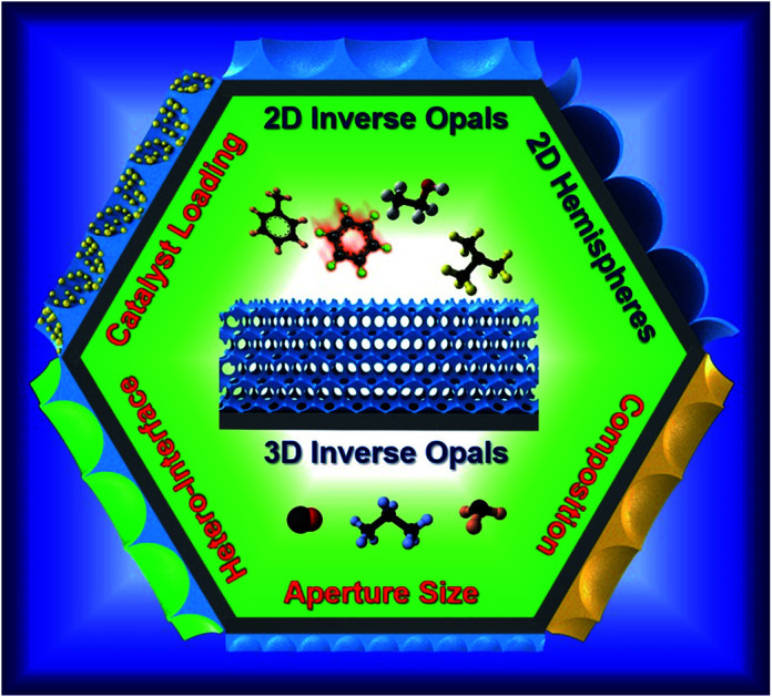
1. Introduction
Reliable monitoring of air quality is currently a concern of the extensive worldwide scientific and technological communities, stimulated by the ever-worsening environmental pollution issues.1 To wean us off this crisis, these communities have developed a range of gas sensors and achieved innovations in sensor technology over the past few decades.2,3 Nowadays, the end use of gas sensors has been largely extended to various fields such as industrial, medical, automotive, petrochemical, military, and food safety.4–6 According to a survey by Grand View Research Inc, the global gas sensor market was valued at USD 1.9 billion in 2017 and is anticipated to reach USD 3.4 billion by 2025; solid-state gas sensors share a major stake (∼30%) of the sensor market.7 Among the various type of sensors, semiconducting metal oxide (SMO) gas sensors as a class of chemiresistive solid-state sensors have gained considerable attention because of their real-time monitoring abilities, as well as other benefits such as low cost, simple working principle, and good compatibility with Si processes.8,9 Metal oxide semiconductors were first commercialized by Figaro for practical utilization in inflammable gases detection in the 1960s. In terms of the majority carrier of metal oxides, SMO sensors can be divided into n-type (e.g., SnO2, In2O3, and WO3) and p-type (e.g., Co3O4, NiO, and CuO).10,11 The working principle of SMO sensors is based on the electric conductance change resulting from the surface interaction between the oxides and analyte gas.12 A study shows that the response of p-type metal oxides is only equal to the square root of the n-type one when both the sensors have the same morphological configurations.13 However, p-type SMO sensors with high catalytic activity are advantageous for detecting a range of new analyte gases with relatively low reactivities.14–16 Therefore, it is not difficult to conclude that both n- and p-type SMO sensors play important roles.
To further enhance the sensing performance, considerable effort has been devoted toward the synthesis of sensing materials with various nanostructures and the analysis of the sensing mechanism. For instance, Güntner et al. demonstrated that sensors preceded by activated alumina particle filters could dramatically enhance isoprene gas selectivity,17 and microporous zeolite membranes placed ahead of metal oxide sensors could decisively contribute toward superior formaldehyde selectivity even under high humidity conditions.18 It is indicated that structural parameters such as the crystallographic structure and morphology can considerably influence the gas-sensing characteristics, particularly the response property, of SMO gas sensors.19–21 As compared to bulk counterparts, nanoarchitectures, such as nanosheets, nanowires, nanoparticles, etc., can facilitate the enhancement of sensing performance due to the increased specific surface area to volume ratio, active surface sites and species (e.g., O2− and O−), and gas adsorption affinity.22–24 For practical gas-sensing utilization, these nanostructures (nanosheets, nanowires, and nanoparticles) need to be fabricated into a macroscopic film on the sensor electrode, usually via drop-casting or brush-coating, making the stability and reliability of gas-sensing properties difficult to be guaranteed.25,26 With this perspective, ordered macroporous nanostructures have been recently considered as worthwhile candidates to resolve the above problems and also attract considerable interest in a range of fields such as photonic crystals, catalysts, and energy storage and conversion technologies.27,28 In principle, the preparation of macroporous materials with aperture sizes in the range from 50 nm to 1.5 μm can increase the gas accessibility and chemical diffusion rate, while the fabrication of a macroscale aperture in an ordered manner can formidably strengthen the sensing stabilities and repeatabilities.29 Moreover, these ordered macroporous nanostructures, usually prepared by polymeric microsphere sacrificial template method, can be a promising platform to perform heteroatom doping, interfacial and surficial tuning, as well as defect engineering to extract the maximum potential out of the oxide material's properties.30 With respect to the influencing factors and enhanced sensing mechanism, many detailed investigations have been carried out on these ordered macroporous nanostructures.
In this review, we provide an overview on the designed syntheses of ordered macroporous metal oxides and summarize the existing protocols for colloidal crystals (CCs), as well as two-dimensional (2D) and three-dimensional (3D) ordered macroporous nanostructures. Furthermore, the key parameters to determine the gas-sensing characteristics of ordered macroporous nanostructures are discussed in relation to the sensing mechanism, which include macro/mesoporosity, heterojunctions, heteroatom dopants, surface adsorption, and their synergistic combinations. Some modification strategies are also demonstrated with a summary of the reported examples. With a better understanding of these topics, the rationales behind their enhanced sensing properties are revealed. Last, but not the least, imminent challenges and future prospects are discussed to provide new insights into the possible development of macroporous materials to be used in gas sensors. It is believed that this review can offer a clear guideline for the design and preparation of macroporous metal oxides with improved sensing performances.
2. Synthesis methods for ordered macroporous nanostructures
2.1. Assembly of CC templates
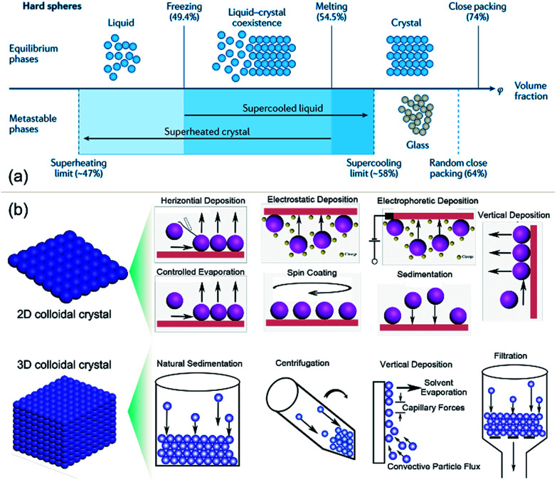
It is well known that ordered macroporous metal oxide nanostructures can be prepared by means of several approaches, such as CC hard template, anodized aluminum oxide template,31,32 and e-beam lithography.33 Among them, studies have popularly focused upon hard spherical template methods due to their facile, controllable, and cost-effective characteristics.34,35 Herein, the main focus of this review is on the CC template method for ordered macroporous oxide nanostructures. The quality of the self-assembled colloidal spherical template plays an important role in fabricating uniform and ordered macroporous arrays. Fig. 1a shows the phase diagrams of monodisperse colloids at different volume fractions (φ). When φ is 74%, monodisperse colloids exhibit a hexagonal close-packed (hcp) structure due to energy minimization, thereby forming CCs.36 Nowadays, 2D or 3D CCs have attracted increasing attention for their wide usage in far-ranging research areas such as photonics, sensors, catalysis, lithography, and bionics.37,38 Till now, a plethora of assembly methods have been developed by the research community, which are being continuously optimized and refined.39,40
Fig. 1. (a) Phase diagrams of monodisperse colloids at different volume fractions. Modified with permission.36 Copyright 2016, Macmillan Publishers Limited. (b) 2D and 3D crystallization methods for close-packed CCs.
Fig. 1b shows different colloidal crystallization methods for the self-assembly of 2D and 3D CCs, namely, horizontal deposition (for 2D CCs), vertical deposition (for 2D and 3D CCs), controlled evaporation (2D CCs), spin-coating (2D CCs), electrostatic deposition (2D CCs), natural sedimentation (3D CCs), and centrifugation (3D CCs).41 Apart from these methods, some liquid interface-mediated methods, such as Langmuir–Blodgett transfer, floating assembly, and air/water interfacial self-assembly, have also been employed to fabricate large-scale monodisperse colloidal spherical crystals and binary colloidal crystals (bCCs).42 For instance, Kotov et al. reported an ethylene-glycol-associated floating self-assembly technique for the first time to prepare 3D CCs with the hcp lattice structure from polystyrene (PS) particles of various diameters (10–240 μm).43 More recently, Dai et al. determined the phase diagram of monolayer bCCs for the rational design and accurately controlled fabrication of bCCs with tuned structures, and they fabricated large-area (>10 cm2) monolayer bCCs based on the ethanol-assisted air/water interfacial self-assembly route.44 Besides these close-packed CCs, a range of 2D and 3D non-close-packed CCs have also been developed by means of plasma treatment, heat treatment, and elastomeric substrate stretching on their close-packed parent crystals.45–47 The flexibility and diversity of CCs can offer us considerable freedom in the fabrication of ordered macroporous nanostructures and their structural engineering for sensing performance tuning.
2.2. Ordered macroporous nanostructures
Ordered porous metal oxides can be universally prepared by impregnation or deposition with guest precursors, followed by heat treatment to remove the template matrix, thereby forming crystalline metal oxide replicas.48,49 Silica spheres, poly(methyl methacrylate) (PMMA) spheres, and PS spheres are used as the representative hard templates for 2D macroporous networks like inverse opals (IOs). After the deposition/coating of the metal oxide materials, the nanospherical template can be removed via annealing in air or etching in some solvents (e.g., CH2Cl2 for PS spheres and NaOH for SiO2 spheres). Using a PMMA template, Kim et al. prepared 2D ordered macroporous (2DOM) CaCu3Ti4O12 thin films by pulsed laser deposition onto PMMA-templated substrates, exhibiting higher surface area, porosity, and permeability toward gases than those exhibited by untemplated films.50 Sputtering methods have also been widely used for fabricating 2DOM nanostructures, for instance, a p-type NiO ordered porous film was prepared by RF sputtering.51 These “top-down” sputtering and deposition techniques provide high controllability over film thickness, channel connectivity, and precise elemental/layer regulation. However, the limited variety of sputtering targets may be a drawback in the broader achievement of different metal oxide compositions on demand; meantime, in certain sputtering methods, polymeric hard spheres cannot survive in a high-temperature environment. Hence, increasing attention has been focused on fabricating 2DOM nanostructures by means of other routes.
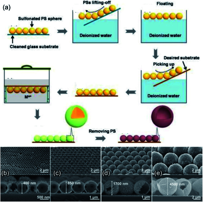
One technique that holds this promise is the solution dipping/permeation strategy that allows for the wide applicability to almost all the soluble metal salts for ordered macroporous metal oxides, and therefore, offers considerable freedom for controlling the composition and hierarchy of metal oxides and compounds.29,52,53 As shown in Fig. 2a, the pre-assembled close-packed PS spheres as the hard template matrix are immersed in a metal salt solution, followed by heat treatment for oxide formation and template removal.48,54 It is found that the PS colloidal monolayer can be peeled off from the substrate and then floated on the water or solution surface, eliminating the dependency on flat substrates.49 For instance, based on the solution-dipping template transfer method, Cai et al. fabricated a series of metal oxides (e.g., In2O3, SnO2, and alpha-Fe2O3) ordered macroporous hollow hemispherical arrays on curved substrates.30,55,56 By impregnation with mixed metal precursors, multicomponent metal oxides can be obtained.57 Based on a stepwise floating–immersing approach (Fig. 2), Su et al. demonstrated the substrate-independent fabrication of hollow spherical arrays with tunable spherical diameters, material systems (Fe2O3, In2O3, NiO, Co3O4, MgO, CuO, ZnO, SnO2, and polyaniline), and shell thickness on the desired substrates including flexible substrates.48 Along with the bCC template, one can also achieve the fabrication of hetero-aperture ordered macroporous arrays.29,30,44 When adding certain colloids (e.g., graphene oxide nanosheets and gold nanoparticles) into the metal salt solution, elegant oxide-based 2D macroporous composites can be obtained, such as SnO2-graphene ordered macroporous thin films.58 Recently, Güntner et al. and Pratsinis et al. developed the flame spray pyrolysis (FSP) method to directly deposit highly porous films with controllable compositions (e.g., Ti:ZnO59 and Si:MoO360) on sensor substrates to build a single sensor61–65 and sensors arrays66–68 for the selective detection of human breath biomarkers. If combined with in situ resistance measurements during deposition, the formation of highly porous networks can be monitored with morphology-dependent resistance patterns to systematically design metal-oxide-based gas sensors with high performances.69
Fig. 2. (a) Schematic illustration of the formation process of ordered metal oxide macroporous hollow spherical arrays. (b–e) Fabricated Fe2O3 hollow spherical arrays with different aperture sizes by using 500, 1000, 2000, and 5000 nm PS spherical templates. Reproduced with permission.48 Copyright 2017, Elsevier Ltd.
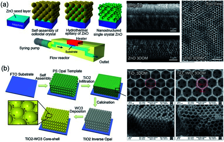
Besides such 2DOM nanostructures, 3D ordered macroporous (3DOM) metal oxides have also been similarly synthesized using 3D CC templates.70–72 When compared with a monolayer 2D counterpart, 3DOM thin films tend to be endowed with strengthened continuous connection channels, as well as improved avenues for conducting electrical signals.73 The preparation of 3DOM metal oxides is often based on the metal precursor solution impregnation.74–76 Miyake et al. recently reported a novel epitaxial growth process of single-crystal 3DOM ZnO through a 3D PS spherical template via a flow-reactor-assisted low-temperature hydrothermal route, exhibiting electrical properties superior to those of polycrystalline ZnO, as shown in Fig. 3a.52 In addition, by adding dopants into metal precursors, multicomponent or doped 3DOM metal oxides can be obtained, such as Pt-doped SnO2,77 Au-doped In2O3,78 and Fe-doped TiO2.79 Combined with some other physical/chemical deposition methods, the heterojunction can be constructed upon the 3DOM structure.80 For example, Ling et al. fabricated a core–shell 3DOM TiO2–WO3 thin film through the electrodeposition of 50 nm-thick WO3 onto uniform 3DOM TiO2 thin films, as shown in Fig. 3b, which can provide a tunable modification of the electrical and optical performances.53
Fig. 3. (a) Flow-reactor-assisted hydrothermal fabrication process and morphologies of 3DOM ZnO. Reproduced with permission.52 Copyright 2017, American Chemical Society. (b) Fabrication process and morphologies of core–shell 3DOM TiO2 and TiO2–WO3. Modified with permission.53 Copyright 2018, Royal Society of Chemistry.
It is worth mentioning that the 3DOM structure can serve as an ideal framework to form a hierarchical porous system. By the combination with some surfactants, an ordered metal oxide hierarchical structure can be realized via CC templating.74 As shown in Fig. 4, a hierarchically ordered mesoporous–macroporous (3DOM/M) TiO2 structure was fabricated with the integration of the triblock copolymer P123 and PS CC.74 This hierarchically porous TiO2 structure exhibits a highly crystalline framework, huge pore volume (≈1.2 cm3 g−1), large surface area (up to 240 m2 g−1), and periodic and highly interconnected pores. A similar example can be found on a 3DOM/M La1−xCexCoO3 perovskite prepared via the combination of meso-molding and colloidal sphere templating.81 It is believed that such a hierarchical porous framework can be a reliable candidate for many functional applications because of its large specific area and pore volume, high gas accessibility, and highly thermal stability.
Fig. 4. (a) Schematic illustration of the formation and (b) microstructure of a hierarchically 3D ordered mesoporous–macroporous TiO2 structure. Reproduced with permission.74 Copyright 2014, Wiley-VCH.
3. Gas-sensing properties of ordered macroporous nanostructures
3.1. 2D macroporous arrays for gas sensing
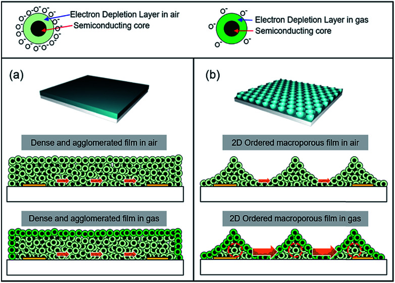
Owing to the above-discussed points, a number of ordered macroporous metal oxide nanostructures have been fabricated for gas sensing over the past years.55,56 Generally, a 2D inverse opal thin film shows distinctive advantages for gas sensing over its dense film counterpart. In a dense and agglomerated sensing film, gas transport to the lower sensing region close to the electrodes becomes difficult (Fig. 5a). For the untemplated dense metal oxide film, the upper layer of the particles with an electron depletion layer (EDL, n-type) or hole accumulation layer (HAL, p-type) is very thin and far away from the bottom electrodes; the conduction of the sensor could be explained by the parallel competition between the thin upper layer with EDL (or HAL) and relatively thick inner layer without EDL (or HAL).54 Because only the particles near the surface participate in the gas-sensing reaction and the inner particles remain inactive, chemiresistive variations become low. In contrast, the 2D inverse opal structures provide high gas accessibility, activating most of the sensing materials and enabling rapid gas response. In particular, the chemiresistive variation at the thinnest region is the highest, which, in turn, significantly increases the overall gas response (Fig. 5b).
Fig. 5. Schematic gas-sensing mechanisms of (a) dense agglomerated films and (b) 2DOM films using n-type oxide chemiresistors.
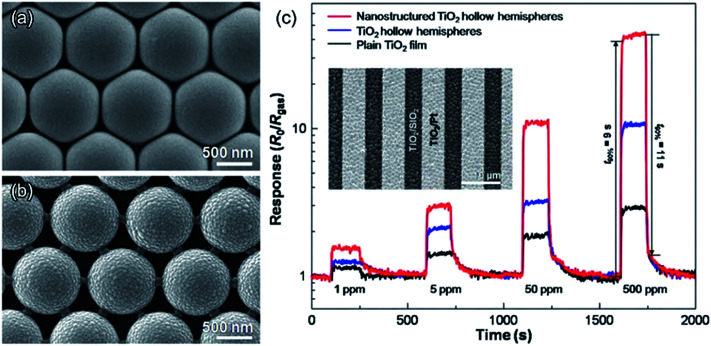
The configuration of the connection between adjacent hollow hemispheres is also an important parameter to modify the gas-sensing characteristics of 2DOM nanostructures.48 Moon et al. prepared two different connecting configurations of TiO2 hollow hemispherical arrays by controlling the plasma etching of 2D hcp PS ball array templates (Fig. 6a and b).82 The CO response increased 4 times by decreasing the contact area between the hollow hemispheres (Fig. 6c) and 10 times in comparison to the plain film. This can also be explained by the high chemiresistive variations at the thin connecting portion.83 The thinner neck width (D) leads to a lower D/λD ratio (λD, Debye length), and the sensor response increases as the D/λD ratio decreases, according to Yamazoe's studies.12 Meanwhile, it is indicated that it becomes easier for gas molecules to access thin nanobridges in ordered nanostructures, which facilitates the sensing process.82–84 The results of both 2D IO structures and 2D hollow hemispheres clearly reveal that the 2DOM nanostructures are promising nanoarchitectures to simultaneously achieve high and rapid response. In addition, the ordered frame matrix would be robust in tolerating the compressive and tensile stresses experienced during the heating/cooling operations due to the more uniform force distribution in ordered porous films, which can yield higher sensing stability. For instance, Xu et al. demonstrated that a 2DOM ZnO sensor can retain the long-term sensing stability for 16 months.85
Fig. 6. Top-view SEM images of (a) TiO2 hollow hemispheres and (b) nanostructured TiO2 hollow hemispheres (pointy contact between hemispheres); (c) sensing transients of plain TiO2 film, hollow hemispheres, and nanostructured hollow hemispheres to 1–500 ppm CO at 250 °C. Reprinted with permission.82 Copyright 2010, Elsevier Ltd.
Currently, a diversity of metal oxide 2DOM films have been in situ constructed on desired sensor substrates to fabricate SMO gas sensors via sputtering and solution-related templating methods.48,54,86 For instance, Xu et al. recently reported a new photochemistry-based solution-dipping method to prepare monolayer macroporous SnO2 arrays with controlled surface pore sizes (varying the UV irradiation time) on ceramic tubes for ethanol sensors, showing rapid response–recovery rate (within 10 s) and high stability for temperatures lower than 300 °C.87 However, the use of wide-spaced electrodes (in millimeters) on ceramic tubes can engender ultrahigh resistance (usually in hundreds of megaohms) in the metal oxide sensing film, which hampers the convenient measurement of sensor resistance using conventional electric circuits.88 In this context, the creation of micro- or nanoscale electrode spacing is considered as an emerging trend to increase the electrical conductance and improve the signal-to-noise ratio of SMO gas sensors. Using a filament as the template, Duan et al. constructed a microgap electrode pair on the ceramic tube to load the 2DOM ZnO IO thin film.79 A microgap ZnO IO sensor showed much lower device resistance and ultralow detection limit to acetone (60 ppb) as compared to normal sensors.
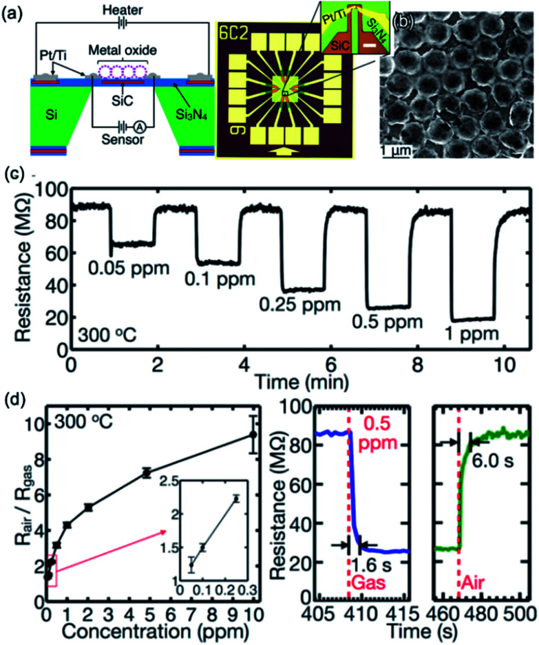
More precise micro/nanogaps and sensors could be achieved by microelectromechanical system (MEMS) processes, which has the potential to become the key sensor device for future practical applications.89,90 For instance, Rao et al. presented the localized on-chip synthesis of 2DOM SnO2 on a MEMS-based microheater platform (Fig. 7a and b).84 The fabricated SnO2 integrated sensor exhibits high sensing performance toward formaldehyde gas at 300 °C (Fig. 7c and d), such as high response, high selectivity, fast response (1.6 s)/recovery (6.0 s) rate, and low detection limit (6.5 ppb).84 Dai et al. also illustrated a similar sensor structure via the fusion of 2DOM SnO2 film and MEMS-based sensing chip that contains micro-spaced interdigital electrodes and low-powered microheaters. The sensor exhibited high ethanol response (ppb level), fast response (<1 s), and low power consumption (32 mW at 350 °C).91,92 As compared to some non-ordered porous films, ordered porous SnO2 sensors can exhibit enhanced response and sensing kinetics,61 but further efforts need to be made toward improving their gas selectivities, such as zeolite membrane filters18 and construction of even orthogonal sensor arrays (E-nose).66
Fig. 7. (a) Schematic diagram and (b) morphology of the as-fabricated sensor with the integration of microheater platform and macroporous SnO2 hollow spherical array. (c) Real-time sensor resistance transient to HCHO at 300 °C. (d) Sensor response versus HCHO concentration, and real-time sensor response and recovery behaviors to 0.5 ppm HCHO. Reproduced with permission.84 Copyright 2017, American Chemical Society.
Although the 2D macroporous configuration and micro-spaced electrode are beneficial to the overall performance, it is still a challenge to realize high-performance gas sensing for pure metal oxides, particularly with regard to selectivity.83,93 Hence, certain modification strategies need be considered, such as heteroatom doping, surface modification, and interfacial engineering, to enhance the sensing of 2DOM metal oxides.94 For instance, the ethanol response and selectivity of 2DOM NiO thin-film sensors are known to significantly increase by Mg doping.95 It should be noted that ethanol sensing on different basic/acidic surfaces undergoes different interaction processes, as shown in reactions (1) and (2).96,97
 |
1 |
 |
2 |
Accordingly, the enhancement of the gas response by MgO doping can be understood in relation to the promotion of ethanol-sensing reaction via dehydrogenation on more basic surfaces.
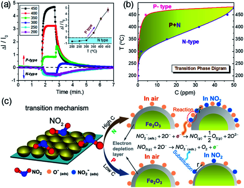
Based on 2DOM Fe2O3 with an amphoteric surface, Dai et al. discovered an abnormal NO2 sensing behavior with reversible transitions from n- to p-type sensing, as shown in Fig. 8a.98 This p–n sensing-type transition has been further revealed to be dependent on the operating temperature (T) and NO2 concentration (C); accordingly, a T–C transition phase diagram was determined (Fig. 8b). Three zones can be observed in the T–C transition diagram, namely, p-type, n-type, and mixed p + n sensing zones, which facilitate the sensing and identification at different T and C levels. Such a T–C transition phase diagram can guide the design of SMO sensors that can be tuned accurately and as desired through an appropriate choice of T and C values. Furthermore, using classical Lennard-Jones (LJ) model, the mechanism for sensing-type transition was effectively explained, where the sensing reactions are different at high and low C conditions, as shown in Fig. 8c.98 A sensing-type transition has also been observed on a MEMS-based n-type 2DOM SnO2 sensor after aging the sensor in 100 ppm ethanol.94 It was discovered that the modified SnO2 sensor exhibited abnormal resistance increase to the reducing sarin gas only at 300 °C, providing a reliable route to distinguish the nerve agent sarin from other reducing interference gases (e.g., dimethyl methylphosphonate, EtOH, and acetone). Such a sensing-type transition can offer us a novel and intriguing avenue for selective and discriminative gas detection.100–102
Fig. 8. (a) NO2 response of 2DOM Fe2O3 at different temperatures (T) and concentrations (C). (b) T–C transition phase diagram. (c) Schematic illustration of different NO2 sensing types at high and low C values, respectively. Reproduced with permission.98 Copyright 2015, Royal Society of Chemistry.
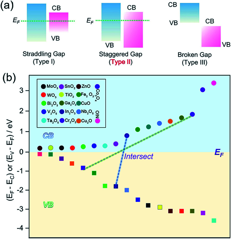
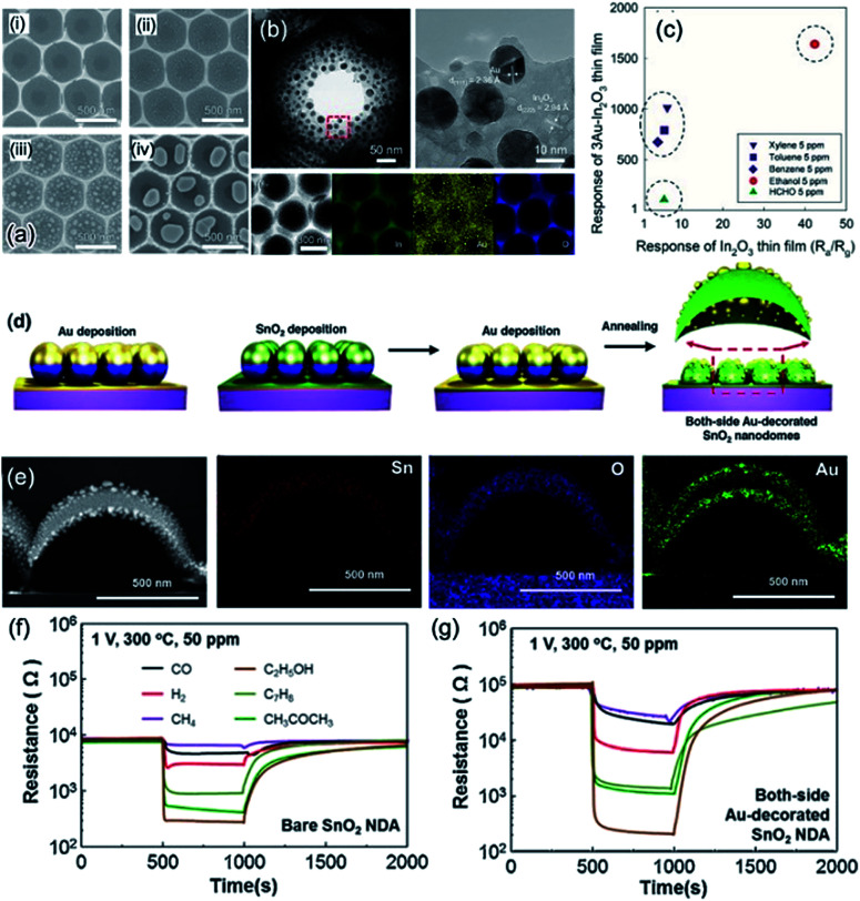
Interfacial engineering is also considered as an elegant alternative to modify the gas-sensing characteristics due to band alignment and altered electronic structures at the interfaces.103,104 For semiconducting oxide–oxide junctions, the interface can be classified into three types of heterojunctions, as shown in Fig. 9a. It is proven that a staggered-gap (type-II) heterojunction facilitates the separation of electron and holes at the interface, enhancing the gas-sensing performance.105,106 The junction diagram (band aligned by Fermi level), as shown in Fig. 9b, can be employed for determining which two oxides can form a type-II heterojunction. In Fig. 9b, only the conduction band–valence band (CB–VB) linking lines of two oxides (e.g., In2O3–Co3O4 couple shown in Fig. 9b) shows an intersection, where a staggered-gap (type-II) heterojunction will be formed. For example, Zhang et al. fabricated 2DOM CuO/In2O3 bilayer 2DOM films via a solution-dipping and sputtering route. With regard to their sensing performance, it was revealed that the CuO/In2O3 p–n junction can obviously improve the gas response and lower the working temperature in comparison to the non-junction counterparts.94 Metal decoration (e.g., Au, Ag, and Pt) on the surface of hollow metal oxide nanostructures can enhance the gas-sensing properties because metal nanoparticles on the surface play the roles of chemical and/or electronic sensitizers.107,108 Recently, Lee et al. developed an ultrafine Au-loaded In2O3 2DOM thin film (Fig. 10a and b) with the solution-dipping template route followed by Au evaporation and beam deposition, demonstrating ultrahigh responses (674.9–1012.9) to 5 ppm benzene, p-xylene, and toluene.103 Further, the sensing responses and selectivities can be easily tuned by the size and spatial distribution of Au nanocatalysts. Based on a simple and reliable algorithm established from the signals of two sensors (Fig. 10c), harmful aromatic VOCs (benzene, xylene, and toluene) could be discriminated from the less toxic ethanol.103 By a range of sputtering or physical vapor deposition (PVD) methods, metals can be uniformly decorated on the 2DOM outer surface,109 but the inner shell could not be utilized for metal loading for further improving its sensing performance. To address this, Shim et al. firstly developed an elegant strategy to realize Au decoration on both sides of 2DOM SnO2 shells, as shown in Fig. 10d; this is clearly verified by the transmission electron microscopy (TEM) images (Fig. 10e).104 Excitingly, such both-side Au-decorated SnO2 2DOM films showed 18 times higher gas response than that by bare SnO2 films, as shown in Fig. 10f and g. Because of the fact that extended EDLs can be formed on both outer and inner surfaces, the total EDL thickness can be maximized when compared with those of single-side-decorated samples, resulting in ultrahigh response to several gases. Apart from Au, Ag, Pt, and Pd can be the other choices of decorations as both chemical and electronic sensitizers.110,111
Fig. 9. (a) Three types of semiconductor heterojunctions organized by band alignment. (b) CB and VB band positions referred to the Fermi level (EC − EF or EV − EF). In the upper portion, the CB position is arranged according to the distance to EF for these oxides; in the bottom part, the VB position is also arranged according to the distance to EF.
Fig. 10. (a) The morphologies of Au-decorated In2O3 2DOM thin films with different Au loading densities. (b) the TEM images and the corresponding elemental mapping. (c) Discriminatory behaviour between ethanol, HCHO and harmful aromatic VOCs (benzene, xylene, and toluene) using two selective sensor responses of Au-In2O3 2DOM sensor and pure dense In2O3 sensor. Reproduced with permission.103 Copyright 2018, Elsevier Ltd. (d) Schematic illustration of the fabrication process for both-side Au-decorated In2O3 2DOM thin films. (e) TEM images and the corresponding elemental mapping of both-side Au-decorated In2O3 2DOM. (f and g) The sensing responses of the both-side Au doped In2O3 and bare In2O3 2DOM gas sensors operating at 300 °C. Reproduced with permission.104 Copyright 2015, Elsevier Ltd.
3.2. 3D macroporous arrays for gas sensing
Because of the similar routes from colloidal templates to ordered macroporous nanostructures, some strategies of 2DOM can be effectively migrated to the 3DOM system. In general, the thickening of the sensing film can deteriorate the transport of the analyte gas to the inner sensing regions close to the electrodes. With this perspective, the gas response can be decreased by changing the structure from 2DOM to 3DOM. On the contrary, certain irreplaceable advantages could be engendered when using 3DOM nanostructures. For instance, a 3DOM film can exhibit higher conductance than that of a 2DOM film owing to the increased material thickness and connectivity. Moreover, the 3D frame matrix would be more robust toward tolerating compressive and tensile stresses during the heating/cooling operations as compared to the fragile 2D ones. Importantly, a 3D periodic array of macropores provides highly interconnected pores. It should be noted that the methanol (500 ppm) response of 3DOM SnO2 with highly periodic macropores is 2.1 times higher than that of the SnO2 porous structure containing the same size of random macropores, clearly confirming that the rapid and effective gas transport to all the sensing surfaces can be obtained with ordered macroporous structures.112 Accordingly, 3DOM is also an attractive nanoarchitecture for fabricating high-performance gas sensors.
Due to the all-in-one formation of 3D CCs, it may be harder to control the pore hierarchy of 3DOM films than those of 2DOM ones. Herein, we will mainly introduce the recent efforts expended by researchers to enhance the sensing performance of metal oxide 3DOM films, such as surficial and interfacial effects.113,114 Metal decoration has also been indicated as a facile way to promote the sensing properties of 3DOM metal oxides. For example, Wang et al. prepared Pd-loaded 3DOM WO3 samples with better sensing performance than pure 3DOM WO3, demonstrating the fact that Pd loading is an effective method to simultaneously improve the gas response (ca. 225 times higher), enhance the selectivity, and reduce the working temperature.115 The synergistic effect between Pd sensitization and structural defects of Pd-loaded 3DOM WO3 nanomaterials leads to dramatically enhanced H2-sensing properties. Similarly, a Pd-loaded 3DOM In2O3 sensor showed enhanced NO2-sensing performance (resistance ratio of 980 to 500 ppb of NO2 at room temperature) due to the Pd-induced surface modification of the EDL thickness.116 A Au-loaded 3DOM In2O3 gas sensor fabricated by Xing et al. was able to detect 5 ppm acetone with response of 42.4 within 11 s at 340 °C in addition to good selectivity, showing promising potential in exhaled breath analysis for diabetes diagnosis. The excellent gas-sensing properties of the Au/In2O3 material could be attributed to the spillover effect between Au and In2O3 and the special 3D IO structure.117
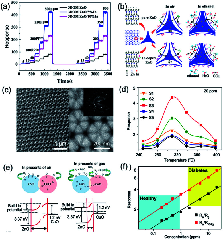
In addition to doping noble metallic nanoparticles, oxide additives can be employed for tuning the gas-sensing characteristics. Rare-earth-(Tm, Er, La, Yb, and Ce)-doped 3DOM In2O3 nanostructures were prepared by a CC templating method by Han et al.118 In particular, Tm-doped 3DOM In2O3 exhibited the best gas-sensing performance, and the gas response for 100 ppm ethanol (122 at 175 °C) was 7 times higher than that of pure 3DOM In2O3. Meantime, Gu and his co-workers prepared In-doped ZnO 3DOM with an aperture size of 150 nm and fabricated a gas sensor with higher response (∼88) to 100 ppm ethanol at 250 °C than that of the nondoped one, as shown in Fig. 11a.113 The enhanced gas response could be attributed to the increase in oxygen adsorption (Fig. 11b). Moreover, the low-temperature active nature of indium could lead to a decrease in the working temperature in addition to improving the ethanol response. A sensor based on Sn-doped 3DOM NiO also showed enhanced formaldehyde-sensing performance, where the substitution of high-valence Sn4+ into Ni2+ enriched the surface-adsorbed oxygen to facilitate the sensing process.119 Alkali-metal (Li+, Na+, K+, Rb+, and Cs+)-doped 3DOM WO3 materials were also prepared using a simple CC template method by Gu et al.120 Among these samples, Li-doped 3DOM WO3 exhibited the highest sensing response of 55 to 500 ppb NO2 at 25 °C along with fast response and excellent selectivity; this could be attributed to the optimized structure defects and carrier mobility of 3DOM WO3/Li. Besides these n-type 3DOM materials, p-type 3DOM metal oxides have been also fabricated, as illustrated by the example of 3DOM La1−xMgxFeO3 fabricated by Qin et al., among which 3DOM La0.95Mg0.05FeO3 shows the optimum methanol response of 146.5 to 100 ppm at 190 °C, as well as good selectivity toward methanol due to the basic surface nature of LaFeO3 material.121
Fig. 11. (a) Dynamic response curves of typical 3DOM samples to different concentrations of ethanol at 250 °C. (b) Schematic diagram of ethanol sensing on the surface of pure and In-doped 3DOM ZnO. Reproduced with permission.113 Copyright 2016, American Chemical Society. (c) Morphologies and microstructure of 3DOM ZnO–CuO arrays. (d) Acetone responses of S1–S5 ZnO–CuO 3DOM sensors as a function of the working temperature; here, Zn/Cu atomic ratios are 1 : 0, 3 : 1, 1 : 1, 1 : 3, and 0 : 1 and marked as samples S1–S5, respectively. (e) Schematic illustration of p–n-junction-enhanced sensing mechanism. (f) Response of S3 ZnO–CuO 3DOM sensor to very low acetone concentration under ∼93.5% RH. Reproduced with permission.114 Copyright 2015, Elsevier Ltd.
In addition, the gas-sensing characteristics of 3DOM nanostructures can also be enhanced or tuned by appropriate heterojunctions of two different kinds of SMOs.122–124 Among them, ZnO–CuO nanocomposites have attracted considerable interest for their capacity toward detecting low-concentration gases.105,125–127 A series of 3DOM ZnO–CuO films with different Zn/Cu atom ratios were synthesized using a simple PMMA template method described by Xie et al., as shown in Fig. 11c.114 By mixing of n-type ZnO and p-type CuO materials, numerous p–n heterojunctions and EDLs are formed at the interface, resulting in a new Fermi level and higher response to acetone gas at 20 ppm (Fig. 11d and e). The excellent sensing performance of 3DOM ZnO–CuO composites shows the promising potential in monitoring and detecting diabetes in a noninvasive and accurate manner (Fig. 11f).114 According to Pratsinis' studies, it should be mentioned that acetone, as a byproduct of fat metabolism, can be altered by exercise63 or ketogenic diet.64 More recently, a series of 3D IO In2O3–ZnO 3DOM heterostructures have been fabricated as n–n junctions.128 Unlike an EDL formed by the p–n junction, the electron at the n–n or p–p interface can migrate into the low-energy CB, changing the charge carrier concentration at the EDL and sequent oxygen adsorption. As a result, a 3DOM ZnO–In2O3 multilayer film with a pore size of 170 nm developed by Wang et al. exhibited improved acetone-sensing properties, such as 2-fold higher response, faster recovery, better selectivity, lower detection limit (332 ppb), and long-term stability.129
3.3. Multimodal porosity control for gas sensing
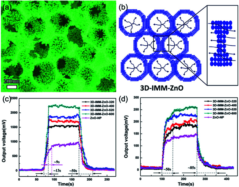
Ordered mesoporous metal oxides are regarded as a type of promising sensing materials for gas sensors because of their high specific surface areas and excellent gas accessibility.130–132 The combination of macro–mesoporous (M/M) structures can not only provide highly connected diffusion channels but also engender surface accessibility, facilitating rapid sensing kinetics and high gas response.133,134 For instance, Liu et al. successfully prepared aperture-controllable 3D interconnected M/M ZnO (3D-IMM-ZnO) nanostructures by template-based layer-by-layer filtration deposition, which showed high specific surface area and interconnected channels between the macropores and mesopores, as shown in Fig. 12a.130 This 3D multimodally ordered porous nanostructure is expected to provide sufficient space and facilitate gas diffusion for gas sensing (Fig. 12b). As shown in Fig. 12c and d, the 3D-IMM-ZnO prepared from 600 nm PMMA spheres (3D-IMM-ZnO-600) has showed better acetone-sensing performance than those of other porous and nonporous ones.130
Fig. 12. (a) Morphology of 3D interconnected macro–mesoporous ZnO (3D-IMM-ZnO) nanostructure. (b) Schematic illustration of 3D-IMM-ZnO for gas sensing. Response and recovery time curves of 3D-IMM-ZnO nanostructures to (c) 100 ppm acetone at 260 °C and (d) 100 ppm methanol at 240 °C. Reproduced with permission.130 Copyright 2016, American Chemical Society.
Although macropores are effective for gas diffusion, the coexistence of mesopores is also very important. For instance, if there are only macropores without mesopores, the lower part of the thicker region (see the dot-circled regions in Fig. 5b) in 2D IO sensor remains inactive. If there are abundant mesopores in addition to macropores, the entire material can participate in the gas-sensing reaction. It should be noted that the gas diffusion coefficient is proportional to the pore diameter in mesopores because the Knudsen diffusion is predominant.135 Therefore, not only the amount and interconnectivity but also the size of the mesopores are important for effective gas transport. A 3DOM LaFeO3 synthesized by the PMMA template method was found to consist of both macropores and mesopores (2–50 nm), facilitating the diffusion of target gases further into the inner regions and exhibiting higher selectivity toward methanol than that by non-ordered LaFeO3.136 More recently, Zhang et al. prepared a 3D ZnO–Fe3O4 IO thin film by the template method, archiving a large surface area due to both macroporous and mesoporous structures in the skeleton.137 The 3DOM/M ZnO–Fe3O4 heterostructure exhibited superior acetone-sensing response with a low detection limit of 100 ppb, relative to a pure ZnO sensor, allowing for the reliable diagnosis of diabetic patients by acetone monitoring.
4. Summary and outlook
The increase in the global sensor market has created new opportunities and challenges for SMO gas sensors; certainly, the successful pursuit of SMO with suitable porous structures might make them more competitive for commercial applications. Here, we have taken an overview of the designed synthesis methods for ordered macroporous metal oxides, and a wide range of ordered macroporous nanostructures have been discussed with a focus on their gas-sensing properties, including 2DOM and 3DOM as well as multimodal IMM structures. It is verified that ordered macroporous nanostructures can considerably facilitate gas diffusion to increase the sensing response and kinetics. To understand the current choices of ordered macroporous nanostructures, their gas-sensing response, response/recovery rate, and detection limit are summarized in Table 1. In general, there are several manners and prospects that might result in enhanced sensing performances of macroporous nanostructures, namely, chemical doping, metal decoration, electrode spacing, surficial and interfacial engineering, and porosity hierarchization. From Table 1, it is also evident that ordered porous structures are not sufficient to endow specific gases with favorable selectivity: the synergies with doping/decoration and interfacial and surficial modifications are necessary to overcome this issue. Another issue is the long-term stability for most of the nanostructured gas sensors, because of the presence of film cracks and resistance drift after operating for a relatively longer time at high temperatures. Although the ordered frame matrix would be robust to tolerate the compressive and tensile stresses to a certain extent during the heating/cooling operations, it is still crucial to investigate novel porous structures and materials capable of sensing at lower temperatures to decrease thermal stresses and power consumption.
Gas-sensing properties of representative ordered macroporous metal oxide materials. Here, the selectivity value is defined with the sensing response ratio of the target gas to the reference gas, and the stability is evaluated with the declining proportion (%) of sensing response within a specified period (month).
| Samples | Template | Pore size (nm) | Temp. (°C) | Target gas | Conc. (ppm) | Gas response | Selectivity value | Stability (%/month) | Res./Rec. time (s) | Ref. |
|---|---|---|---|---|---|---|---|---|---|---|
| Close-network ZnO | PS spheres | 400 | 25 | NO2 | 50 | 27.5 | 213.75 to ethanol | — | 35/65 | 48 |
| Bowl-like ZnO | PS spheres | 280 | 25 | NO2 | 50 | 4.5 | 2.25 to ethanol | — | 125/210 | |
| Ordered SnO2 | PS spheres | 200 | 350 | Ethanol | 3 | 3.9 | 1.625 to acetone | −11.8/6 | 0.73/— | 91 |
| Porous LaFeO3 | PS spheres | 500 | 450 | Ethanol | 5 | 15 | 3.21 to HCHO | — | 6/5 | 97 |
| 2D hollow SnO2 | PS spheres | ∼1000 | 300 | HCHO | 0.5 | 23 | 3.67 to CH4 | — | 1.8/5.4 | 84 |
| 2D porous ZnO | PS spheres | 420 | 300 | Acetone | 10 | 17 | 1.7 to ethanol | −5/6 | —/— | 85 |
| Ordered SnO2 | PS spheres | ∼500 | 350 | Ethanol | 0.1 | 1.24 | — | — | 1/1 | 92 |
| Bowl-like SnO2 | PS spheres | 500 | 300 | Ethanol | 1 | 4.3 | — | −48/2 | 2/2 | 90 |
| α-Fe2O3 IO film | PS spheres | 500 | 400 | NO2 | 5 | — | — | −4.2/1 | 12/— | 98 |
| Embossed TiO2 | PS beads | 1000 | 250 | Ethanol | 500 | 219 | 4.38 to CO | — | 10/— | 83 |
| Monolayer Mg–NiO | PS spheres | 700 | 325 | Ethanol | 100 | 10.4 | 6.5 to benzene | −10.6/1 | 13/19 | 95 |
| Au–SnO2: 5% In | PMMA spheres | 250 | 275 | Ethanol | 100 | 292 | 41.71 to MeOH | — | 7/12 | 108 |
| Hollow Pt–SnO2 | PMMA spheres | 800 | 250 | H2 | 250 | 4.08 | — | — | 31/— | 86 |
| Ethanol-aged SnO2 | PS spheres | 500 | 400 | Sarin | 0.006 | 40 | 1.2 to DMMP | — | —/— | 99 |
| Porous In2O3/CuO | PS spheres | 450 | 250 | Ethanol | 1000 | 9.6 | 5.33 to CO | — | 48 | 94 |
| 2D Au/In2O3 | PS spheres | 500 | 350 | Ethanol | 5 | 1640.2 | 282.79 to HCHO | — | —/— | 103 |
| 3D IO SnO2 | PMMA spheres | 400 | 215 | HCHO | 100 | 629 | 104.83 to ethanol | −6/2 | 12/58 | 71 |
| 3D IO WO3 | PMMA spheres | 422.2 | 370 | Acetone | 5 | 7 | 3.89 to MeOH | — | 10/34 | 76 |
| 3DOM Tm–In2O3 | PMMA spheres | 200 | 175 | Ethanol | 100 | 122 | 7.63 to acetone | −2.4/1 | 9/13 | 118 |
| 3DOM Sn–NiO | PMMA spheres | 200 | 225 | HCHO | 100 | 145 | 96.7 to NO2 | −2.1/1 | 30/160 | 119 |
| 3DOM In–ZnO | PMMA spheres | 150 | 250 | Ethanol | 100 | 88 | 1.83 to acetone | — | 25/10 | 113 |
| 3DOM Li–WO3 | PMMA spheres | ∼330 | 25 | NO2 | 0.5 | 55 | 42.31 to NH3 | −9.1/1 | 100/100 | 120 |
| 3DOM Li/K–WO3 | PMMA spheres | 200 | 25 | NO2 | 0.5 | 4.5 | 4.09 to NH3 | — | 15/10 | 138 |
| 3DOM Pd/In2O3 | PMMA spheres | 210 | 25 | NO2 | 0.5 | 980 | 196 to NH3 | 0/1 | 270/286 | 123 |
| 3D IO Au/In2O3 | PMMA spheres | 420 | 340 | Acetone | 5 | 42.4 | 10.6 to ethanol | — | —/— | 117 |
| 3DOM Au/In2O3 | PMMA spheres | 140 | 230 | Ethanol | 100 | 205 | 6.83 to MeOH | — | 15/21 | 78 |
| 3DOM Pd/WO3 | PMMA spheres | ∼330 | 130 | H2 | 50 | 382 | 191 to HCHO | −1/1 | 10/50 | 115 |
| 3D IO ZnO–In2O3 | PS spheres | 170 | 300 | Acetone | 100 | 35.2 | 25.14 to benzene | −9.1/1 | 1/— | 129 |
| 3D IO In2O3–CuO | PMMA spheres | 410 | 370 | Acetone | 50 | 39.1 | 9.5 to ethanol | −2.8/1.3 | 8/20 | 124 |
| 3DOM ZnO–CuO | PMMA spheres | 282 | 310 | Acetone | 1 | 1.8 | 1.53 to toluene | −11/1 | —/— | 114 |
| 3D IO PdO@In2O3 | PS spheres | 636.6 | 250 | Acetone | 100 | 50.9 | 11.31 to C6H6 | −11.6/1 | —/26 | 139 |
| 3DOM/M LaFeO3 | PMMA spheres | 191/8–20 | 190 | Methanol | 100 | 96 | 2.44 to ethanol | — | 25/23 | 140 |
| 3DOM/M-SnO2 | PS spheres | 100/20/3 | 400 | Ethanol | 5 | 316.5 | 3.50 to ethanol | — | 1/416 | 141 |
| 3DOM/M-ZnO | PMMA spheres | 600/25 | 260 | Acetone | 100 | 137 | — | — | 13/50 | 130 |
| 3DOM/M In2O3–ZnO | PS spheres | 80/4 | 25 | NO2 | 5 | 54.3 | 6.9 to MeOH | — | 586/188 | 128 |
| 3DOM/M Pt–SnO2 | Electrosprayed spheres | 300/17 | 250 | H2S | 1 | 10.8 | — | — | 192.4/76.5 | 142 |
| 3DOM/M ZnO–Fe3O4 | PMMA spheres | 350/30 | 485 | Acetone | 50 | 47 | 8.44 to C5H12 | — | —/— | 137 |
Encouragingly, the optimization of connecting channels and electrical conductivity are suggested as an effective means to improve the gas sensing of ordered macroporous metal oxides. Hybridization with highly conductive additives, such as MXene, graphene, and CNTs may greatly promote the charge-transport kinetics and transmission efficiency from surface chemical reaction into readable chemiresistivity signals. In addition, the combinations of different nonmetal element (e.g., S, F, or N) groups to form a solid solution may open up the novel possibility of controlling charge carrier concentrations and chemiresistivity. With respect to porosity, different gas diffusion mechanisms result in different porous structures, such as normal for macropores, Knudsen mechanism for mesopores, and surface diffusion for micropores; hence, the construction of trimodally ordered porous nanostructures that contain macroporous matrixes, mesopores, and micropores can prove to be another elegant route toward the complete utilization of sensing materials. The coating of microporous membranes on macroporous metal oxides can shutter gas molecules with molecular sizes greater than those of open micropores (<2 nm), allowing smaller molecules for gas selectivity. In this regard, some microporous materials such as metal–organic frameworks (MOFs) and covalent organic frameworks (COFs) could be considered.
However, there are still certain scientific and practical issues that need to be resolved. Till now, the mechanistic detail of SMO gas sensing is still an open question. New concepts in the fundamentals of ordered macroporous nanostructures are expected to be revealed for the community. Some tools that hold promise in this context are operando spectroscopies such as in situ solid NMR and in situ FT-IR, which may reveal how sensing properties can be affected by different factors. In practice, one of the most important concerns is the working temperature. For SMO sensors, the working temperature range is between 150 and 400 °C. Highly integrated MEMS sensor or sensor arrays can be employed to decrease the power consumption. For thermally stable 2DOM or 3DOM structures, the sensing materials should be heat-treated at elevated temperatures (e.g., higher than the sensing temperature). Hence, 2DOM and 3DOM structures should be maintained during thermal annealing and long-term sensor operations. The exploration of new porous nanostructures and novel functionalization should be taken into account for further efforts. Overall, it is still imperative to investigate solutions that can bridge fundamental research studies and commercial interests.
Conflicts of interest
There are no conflicts to declare.
Supplementary Material
Acknowledgments
We acknowledge the funding supports from the National Natural Science Foundation of China (Grant No. 51802252), National Research Foundation of Korea (No. 2016R1A2A1A05005331), Natural Science Foundation of Jiangsu Province (No. BK20180237), Young Talents Support Plan of Xi'an Jiaotong University, Fundamental Research Funds for the Central Universities (No. xjj2018001).
Biographies
Biography
Zhengfei Dai.

Zhengfei Dai received his PhD from the University of Chinese Academy of Sciences in July 2013. Then, he worked at the Department of Materials Science & Engineering, Korea University, South Korea. Since December 2014, he has worked at the Department of Chemistry, Kyoto University, Japan, as a JSPS research fellow. From February 2016, he has worked as a research fellow in the Department of Materials Science & Engineering, Nanyang Technological University, Singapore. He joined the School of Material Science and Engineering, Xi'an Jiaotong University, as a faculty member in December 2017. His current research interests focus on gas sensors, secondary batteries, and electrocatalysts.
Biography
Tingting Liang.

Tingting Liang received her B.S. and M.S. degrees from the School of Materials Science and Engineering, Henan University of Science and Technology, in 2014 and 2018, respectively. Now, she is a doctoral candidate of Xi'an Jiaotong University, and she is conducting research on the fabrication and performance of gas sensor devices using nanostructured materials.
Biography
Jong-Heun Lee.

Jong-Heun Lee is a professor in the Materials Science and Engineering department at Korea University. He received his B.S., M.S., and PhD degrees from Seoul National University in 1987, 1989, and 1993, respectively. He developed automotive air–fuel ratio sensors at the Samsung Advanced Institute of Technology during 1993–1999. He was a STA fellow at the National Institute for Research in Inorganic Materials (currently NIMS, Japan) during 1999–2000, and he was a research professor at Seoul National University from 2000 to 2003. He has been a faculty member at Korea University since 2003. His current research interests include chemical sensors and functional oxide nanostructures.
Notes and references
- Stephens G. L. Li J. Wild M. Clayson C. A. Loeb N. Kato S. L'Ecuyer T. Stackhouse Jr P. W. Lebsock M. Andrews T. Nat. Geosci. 2012;5:691–696. doi: 10.1038/ngeo1580. [DOI] [Google Scholar]
- Ma R.-M. Ota S. Li Y. Yang S. Zhang X. Nat. Nanotechnol. 2014;9:600–604. doi: 10.1038/nnano.2014.135. [DOI] [PubMed] [Google Scholar]
- Suehle J. S. Cavicchi R. E. Gaitan M. Semancik S. IEEE Electron Device Lett. 1993;14:118–120. [Google Scholar]
- Righettoni M. Amann A. Pratsinis S. E. Mater. Today. 2015;18:163–171. doi: 10.1016/j.mattod.2014.08.017. [DOI] [Google Scholar]
- Jun J. Lee J. S. Shin D. H. Oh J. Kim W. Na W. Jang J. J. Mater. Chem. A. 2017;5:17335–17340. doi: 10.1039/C7TA02725G. [DOI] [Google Scholar]
- Li C. Krewer G. W. Ji P. Scherm H. Kays S. J. Postharvest Biol. Technol. 2010;55:144–149. doi: 10.1016/j.postharvbio.2009.11.004. [DOI] [Google Scholar]
- Grand View Research, Inc., Gas Sensor Market Size & Share, Industry Analysis Report, 2018–2025, https://www.grandviewresearch.com/industry-analysis/gas-sensors-market
- Barsan N. Koziej D. Weimar U. Sens. Actuators, B. 2007;121:18–35. doi: 10.1016/j.snb.2006.09.047. [DOI] [Google Scholar]
- Zhou Q. Sussman A. Chang J. Dong J. Zettl A. Mickelson W. Sens. Actuators, A. 2015;223:67–75. doi: 10.1016/j.sna.2014.12.005. [DOI] [Google Scholar]
- Eranna G. Joshi B. Runthala D. Gupta R. Crit. Rev. Solid State Mater. Sci. 2004;29:111–188. doi: 10.1080/10408430490888977. [DOI] [Google Scholar]
- Zhang J. Liu X. Neri G. Pinna N. Adv. Mater. 2016;28:795–831. doi: 10.1002/adma.201503825. [DOI] [PubMed] [Google Scholar]
- Yamazoe N. Sakai G. Shimanoe K. Catal. Surv. Asia. 2003;7:63–75. doi: 10.1023/A:1023436725457. [DOI] [Google Scholar]
- Barsan N. Simion C. Heine T. Pokhrel S. Weimar U. J. Electroceram. 2009;25:11–19. doi: 10.1007/s10832-009-9583-x. [DOI] [Google Scholar]
- Kim H.-J. Lee J.-H. Sens. Actuators, B. 2014;192:607–627. doi: 10.1016/j.snb.2013.11.005. [DOI] [Google Scholar]
- Rai P. Yoon J.-W. Jeong H.-M. Hwang S.-J. Kwak C.-H. Lee J.-H. Nanoscale. 2014;6:8292–8299. doi: 10.1039/C4NR01906G. [DOI] [PubMed] [Google Scholar]
- Kim T.-H. Yoon J.-W. Kang Y. C. Abdel-Hady F. Wazzan A. Lee J.-H. Sens. Actuators, B. 2017;240:1049–1057. doi: 10.1016/j.snb.2016.09.098. [DOI] [Google Scholar]
- van den Broek J. Güntner A. T. Pratsinis S. E. ACS Sens. 2018;3:677–683. doi: 10.1021/acssensors.7b00976. [DOI] [PubMed] [Google Scholar]
- Güntner A. T. Abegg S. Wegner K. Pratsinis S. E. Sens. Actuators, B. 2018;257:916–923. doi: 10.1016/j.snb.2017.11.035. [DOI] [Google Scholar]
- Korotcenkov G. Mater. Sci. Eng., R. 2008;61:1–39. doi: 10.1016/j.mser.2008.02.001. [DOI] [Google Scholar]
- Brinzari V. Korotcenkov G. Golovanov V. Thin Solid Films. 2001;391:167–175. doi: 10.1016/S0040-6090(01)00978-6. [DOI] [Google Scholar]
- Korotcenkov G. Macsanov V. Brinzari V. Tolstoy V. Schwank J. Cornet A. Morante J. Thin Solid Films. 2004;467:209–214. doi: 10.1016/j.tsf.2004.03.028. [DOI] [Google Scholar]
- Choi J.-K. Hwang I.-S. Kim S.-J. Park J.-S. Park S.-S. Jeong U. Kang Y. C. Lee J.-H. Sens. Actuators, B. 2010;150:191–199. doi: 10.1016/j.snb.2010.07.013. [DOI] [Google Scholar]
- Kim H. R. Haensch A. Kim I. D. Barsan N. Weimar U. Lee J. H. Adv. Funct. Mater. 2011;21:4456–4463. doi: 10.1002/adfm.201101154. [DOI] [Google Scholar]
- Jeong S.-Y. Yoon J.-W. Kim T.-H. Jeong H.-M. Lee C.-S. Kang Y. C. Lee J.-H. J. Mater. Chem. A. 2017;5:1446–1454. doi: 10.1039/C6TA09397C. [DOI] [Google Scholar]
- Chandra L. Dwivedi R. Mishra V. Mater. Res. Express. 2017;4:105030. doi: 10.1088/2053-1591/aa8dc0. [DOI] [Google Scholar]
- Li F. Guo S. Shen J. Shen L. Sun D. Wang B. Chen Y. Ruan S. Sens. Actuators, B. 2017;238:364–373. doi: 10.1016/j.snb.2016.07.021. [DOI] [Google Scholar]
- Zhao H. Wu M. Liu J. Deng Z. Li Y. Su B.-L. Appl. Catal., B. 2016;184:182–190. doi: 10.1016/j.apcatb.2015.11.018. [DOI] [Google Scholar]
- Armstrong E. O'Dwyer C. J. Mater. Chem. C. 2015;3:6109–6143. doi: 10.1039/C5TC01083G. [DOI] [Google Scholar]
- Jia L. C. Cai W. P. Wang H. Q. Sun F. Q. Li Y. ACS Nano. 2009;3:2697–2705. doi: 10.1021/nn900454k. [DOI] [PubMed] [Google Scholar]
- Jia L. C. Cai W. P. Adv. Funct. Mater. 2010;20:3765–3773. doi: 10.1002/adfm.201001216. [DOI] [Google Scholar]
- Yu J. Wang F. Wang Y. Gao H. Li J. Wu K. Chem. Soc. Rev. 2010;39:1513–1525. doi: 10.1039/B812787P. [DOI] [PubMed] [Google Scholar]
- Wen L. Xu R. Mi Y. Lei Y. Nat. Nanotechnol. 2016;12:244–250. doi: 10.1038/nnano.2016.257. [DOI] [PubMed] [Google Scholar]
- Dravid V. P. J. Mater. Chem. 2009;19:4295–4299. doi: 10.1039/B903201K. [DOI] [Google Scholar]
- Velev O. D. Lenhoff A. M. Curr. Opin. Colloid Interface Sci. 2000;5:56–63. doi: 10.1016/S1359-0294(00)00039-X. [DOI] [Google Scholar]
- Malgras V. Ji Q. Kamachi Y. Mori T. Shieh F.-K. Wu K. C.-W. Ariga K. Yamauchi Y. Bull. Chem. Soc. Jpn. 2015;88:1171–1200. doi: 10.1246/bcsj.20150143. [DOI] [Google Scholar]
- Li B. Zhou D. Han Y. Nat. Rev. Mater. 2016;1:15011. doi: 10.1038/natrevmats.2015.11. [DOI] [Google Scholar]
- Li Y. Duan G. Liu G. Cai W. Chem. Soc. Rev. 2013;42:3614–3627. doi: 10.1039/C3CS35482B. [DOI] [PubMed] [Google Scholar]
- Kuang M. Wang J. Jiang L. Chem. Soc. Rev. 2016;45:6833–6854. doi: 10.1039/C6CS00562D. [DOI] [PubMed] [Google Scholar]
- Tan A. T. L. Beroz J. Kolle M. Hart A. J. Adv. Mater. 2018;30:1803620. doi: 10.1002/adma.201803620. [DOI] [PubMed] [Google Scholar]
- Karg M. König T. A. Retsch M. Stelling C. Reichstein P. M. Honold T. Thelakkat M. Fery A. Mater. Today. 2015;18:185–205. doi: 10.1016/j.mattod.2014.10.036. [DOI] [Google Scholar]
- Vogel N. Retsch M. Fustin C. A. Del Campo A. Jonas U. Chem. Rev. 2015;115:6265–6311. doi: 10.1021/cr400081d. [DOI] [PubMed] [Google Scholar]
- Lotito V. Zambelli T. Adv. Colloid Interface Sci. 2017;246:217–274. doi: 10.1016/j.cis.2017.04.003. [DOI] [PubMed] [Google Scholar]
- Liu Y. Wang S. Lee J. W. Kotov N. A. Chem. Mater. 2005;17:4918–4924. doi: 10.1021/cm048050g. [DOI] [Google Scholar]
- Dai Z. Li Y. Duan G. Jia L. Cai W. ACS Nano. 2012;6:6706–6716. doi: 10.1021/nn3013178. [DOI] [PubMed] [Google Scholar]
- Lee G. H. Choi T. M. Kim B. Han S. H. Lee J. M. Kim S.-H. ACS Nano. 2017;11:11350–11357. doi: 10.1021/acsnano.7b05885. [DOI] [PubMed] [Google Scholar]
- Huang X. Bjork M. Ratchford D. C. Yeom J. Langmuir. 2017;33:12218–12226. doi: 10.1021/acs.langmuir.7b02338. [DOI] [PubMed] [Google Scholar]
- Wendisch F. J. Oberreiter R. Salihovic M. Elsaesser M. S. Bourret G. R. ACS Appl. Mater. Interfaces. 2017;9:3931–3939. doi: 10.1021/acsami.6b14226. [DOI] [PubMed] [Google Scholar]
- Su X. Gao L. Zhou F. Duan G. Sens. Actuators, B. 2017;251:74–85. doi: 10.1016/j.snb.2017.05.024. [DOI] [Google Scholar]
- Sun F. Q. Cai W. P. Li Y. Jia L. C. Lu F. Adv. Mater. 2005;17:2872–2877. doi: 10.1002/adma.200500936. [DOI] [Google Scholar]
- Kim I. D. Rothschild A. Hyodo T. Tuller H. L. Nano Lett. 2006;6:193–198. doi: 10.1021/nl051965p. [DOI] [PubMed] [Google Scholar]
- Cho N. G. Hwang I. S. Kim H. G. Lee J. H. Kim I. D. Sens. Actuators, B. 2011;155:366–371. doi: 10.1016/j.snb.2010.12.031. [DOI] [Google Scholar]
- Miyake M. Suginohara M. Narahara N. Hirato T. Braun P. V. Chem. Mater. 2017;29:9734–9741. doi: 10.1021/acs.chemmater.7b03466. [DOI] [Google Scholar]
- Ling H. Yeo L. P. Wang Z. Li X. Mandler D. Magdassi S. Tok A. I. Y. J. Mater. Chem. C. 2018;6:8488–8494. doi: 10.1039/C8TC01954A. [DOI] [Google Scholar]
- Lee C. S. Dai Z. Jeong S. Y. Kwak C. H. Kim B. Y. Kim do H. Jang H. W. Park J. S. Lee J. H. Chem.–Eur. J. 2016;22:7102–7107. doi: 10.1002/chem.201505210. [DOI] [PubMed] [Google Scholar]
- Wang Y. Y. Duan G. T. Zhu Y. D. Zhang H. W. Xu Z. K. Dai Z. F. Cai W. P. Sens. Actuators, B. 2016;228:74–84. doi: 10.1016/j.snb.2016.01.002. [DOI] [Google Scholar]
- Xu Z. K. Duan G. T. Kong M. G. Su X. S. Cai W. P. ChemistrySelect. 2016;1:2377–2382. doi: 10.1002/slct.201600163. [DOI] [Google Scholar]
- Jia L. C. Cai W. P. Wang H. Q. Appl. Phys. Lett. 2010;96:103115. doi: 10.1063/1.3358389. [DOI] [Google Scholar]
- Xu S. P. Sun F. Q. Yang S. M. Pan Z. Z. Long J. F. Gu F. L. Sci. Rep. 2015;5:8939. doi: 10.1038/srep08939. [DOI] [PMC free article] [PubMed] [Google Scholar]
- Güntner A. T. Pineau N. J. Chie D. Krumeich F. Pratsinis S. E. J. Mater. Chem. B. 2016;4:5358–5366. doi: 10.1039/C6TB01335J. [DOI] [PubMed] [Google Scholar]
- Güntner A. T. Righettoni M. Pratsinis S. E. Sens. Actuators, B. 2016;223:266–273. doi: 10.1016/j.snb.2015.09.094. [DOI] [Google Scholar]
- Righettoni M. Tricoli A. Pratsinis S. E. Anal. Chem. 2010;82:3581–3587. doi: 10.1021/ac902695n. [DOI] [PubMed] [Google Scholar]
- Schon S. Theodore S. J. Güntner A. T. Sens. Actuators, B. 2018;273:1780–1785. doi: 10.1016/j.snb.2018.07.094. [DOI] [Google Scholar]
- Güntner A. T. Sievi N. A. Theodore S. J. Gulich T. Kohler M. Pratsinis S. E. Anal. Chem. 2017;89:10578–10584. doi: 10.1021/acs.analchem.7b02843. [DOI] [PubMed] [Google Scholar]
- Güntner A. T. Kompalla J. F. Landis H. Theodore S. J. Geidl B. Sievi N. A. Kohler M. Pratsinis S. E. Gerber P. A. Sensors. 2018;18:3655. doi: 10.3390/s18113655. [DOI] [PMC free article] [PubMed] [Google Scholar]
- Yoo R. Güntner A. T. Park Y. Rim H. J. Lee H. S. Lee W. Sens. Actuators, B. 2019;283:107. doi: 10.1016/j.snb.2018.12.001. [DOI] [Google Scholar]
- Pineau N. J. Kompalla J. F. Güntner A. T. Pratsinis S. E. Microchim. Acta. 2018;185:563. doi: 10.1007/s00604-018-3104-z. [DOI] [PubMed] [Google Scholar]
- Güntner A. T. Koren V. Chikkadi K. Righettoni M. Pratsinis S. E. ACS Sens. 2016;1:528–535. doi: 10.1021/acssensors.6b00008. [DOI] [Google Scholar]
- Güntner A. T. Pineau N. J. Mochalski P. Wiesenhofer H. Agapiou A. Mayhew C. A. Pratsinis S. E. Anal. Chem. 2018;90:4940–4945. doi: 10.1021/acs.analchem.8b00237. [DOI] [PMC free article] [PubMed] [Google Scholar]
- Blattmann C. O. Güntner A. T. Pratsinis S. E. ACS Appl. Mater. Interfaces. 2017;9:23926–23933. doi: 10.1021/acsami.7b04530. [DOI] [PubMed] [Google Scholar]
- Scott R. W. J. Yang S. M. Chabanis G. Coombs N. Williams D. E. Ozin G. A. Adv. Mater. 2001;13:1468–1472. doi: 10.1002/1521-4095(200110)13:19<1468::AID-ADMA1468>3.0.CO;2-O. [DOI] [Google Scholar]
- Xing R. Q. Xu L. Zhu Y. S. Song J. Qin W. F. Dai Q. L. Liu D. L. Song H. W. Sens. Actuators, B. 2013;188:235–241. doi: 10.1016/j.snb.2013.07.024. [DOI] [Google Scholar]
- Wang Y. Aurelio D. Li W. Tseng P. Zheng Z. Li M. Kaplan D. L. Liscidini M. Omenetto F. G. Adv. Mater. 2017;29:1702769. doi: 10.1002/adma.201702769. [DOI] [PubMed] [Google Scholar]
- Phillips K. R. Shirman T. Shirman E. Shneidman A. V. Kay T. M. Aizenberg J. Adv. Mater. 2018;30:e1706329. doi: 10.1002/adma.201706329. [DOI] [PubMed] [Google Scholar]
- Zhang R. Shen D. Xu M. Feng D. Li W. Zheng G. Che R. Elzatahry A. A. Zhao D. Adv. Energy Mater. 2014;4:1301725. doi: 10.1002/aenm.201301725. [DOI] [Google Scholar]
- Liu L. Liu C. B. Li S. C. Wang L. Y. Shan H. Zhang X. B. Guan H. Y. Liu Z. Sens. Actuators, B. 2013;177:893–897. doi: 10.1016/j.snb.2012.11.106. [DOI] [Google Scholar]
- Xing R. Q. Du Y. Zhao X. N. Zhang X. Sensors. 2017;17:710. doi: 10.3390/s17040710. [DOI] [PMC free article] [PubMed] [Google Scholar]
- D'Arienzo M. Armelao L. Cacciamani A. Mari C. M. Polizzi S. Ruffo R. Scotti R. Testino A. Wahba L. Morazzoni F. Chem. Mater. 2010;22:4083–4089. doi: 10.1021/cm100866g. [DOI] [Google Scholar]
- Gu F. B. Nie R. Tian Z. W. Han D. M. Wang Z. H. RSC Adv. 2015;5:99018–99022. doi: 10.1039/C5RA19525J. [DOI] [Google Scholar]
- Yan X. Xue C. Yang B. Yang G. Appl. Surf. Sci. 2017;394:248–257. doi: 10.1016/j.apsusc.2016.10.077. [DOI] [Google Scholar]
- Tian P. Shen K. Chen J. Fan T. Fang R. Li Y. Small Methods. 2018;2:1800219. doi: 10.1002/smtd.201800219. [DOI] [Google Scholar]
- Arandiyan H. Scott J. Wang Y. Dai H. Sun H. Amal R. ACS Appl. Mater. Interfaces. 2016;8:2457–2463. doi: 10.1021/acsami.5b11050. [DOI] [PubMed] [Google Scholar]
- Moon H. G. Shim Y.-S. Jang H. W. Kim J.-S. Choi K. J. Kang C.-Y. Choi J.-W. Park H.-H. Yoon S.-J. Sens. Actuators, B. 2010;149:116–121. doi: 10.1016/j.snb.2010.06.014. [DOI] [Google Scholar]
- Moon H. G. Shim Y.-S. Su D. Park H.-H. Yoon S.-J. Jang H. W. J. Phys. Chem. C. 2011;115:9993–9999. doi: 10.1021/jp2020325. [DOI] [Google Scholar]
- Rao A. Long H. Harley-Trochimczyk A. Pham T. Zettl A. Carraro C. Maboudian R. ACS Appl. Mater. Interfaces. 2017;9:2634–2641. doi: 10.1021/acsami.6b12677. [DOI] [PubMed] [Google Scholar]
- Xu Z. K. Duan G. T. Zhang H. W. Wang Y. Y. Xu L. Cai W. P. Nanoscale. 2015;7:14264–14271. doi: 10.1039/C5NR02099A. [DOI] [PubMed] [Google Scholar]
- Cho N. G. Whitfield G. C. Yang D. J. Kim H. G. Tuller H. L. Kim I. D. J. Electrochem. Soc. 2010;157:J435–J439. doi: 10.1149/1.3489949. [DOI] [Google Scholar]
- Xu S. P. Sun F. Q. Gu F. L. Zuo Y. B. Zhang L. H. Fan C. F. Yang S. M. Li W. S. ACS Appl. Mater. Interfaces. 2014;6:1251–1257. doi: 10.1021/am4050844. [DOI] [PubMed] [Google Scholar]
- Bläser G. Rühl T. Diehl C. Ulrich M. Kohl D. Phys. A. 1999;266:218–223. doi: 10.1016/S0378-4371(98)00595-0. [DOI] [Google Scholar]
- Guo L. F. Xu L. Xu Z. K. Duan G. T. Wang Y. Zhou H. Liu Y. X. Cai W. P. Wang Y. L. Li T. Microsyst. Technol. 2017;23:2699–2705. doi: 10.1007/s00542-016-3091-0. [DOI] [Google Scholar]
- Guo L. F. Xu L. Xu Z. K. Duan G. T. Wang Y. Cai W. P. Wang Y. L. Li T. Sens. Actuators, B. 2016;231:450–457. doi: 10.1016/j.snb.2016.03.028. [DOI] [Google Scholar]
- Dai Z. F. Xu L. Duan G. T. Li T. Zhang H. W. Li Y. Wang Y. Wang Y. L. Cai W. P. Sci. Rep. 2013;3:1669. doi: 10.1038/srep01669. [DOI] [PMC free article] [PubMed] [Google Scholar]
- Xu L. Dai Z. F. Duan G. T. Guo L. F. Wang Y. Zhou H. Liu Y. X. Cai W. P. Wang Y. L. Li T. Sci. Rep. 2015;5:10507. doi: 10.1038/srep10507. [DOI] [PMC free article] [PubMed] [Google Scholar]
- Su X. S. Duan G. T. Xu Z. K. Zhou F. Cai W. P. J. Colloid Interface Sci. 2017;503:150–158. doi: 10.1016/j.jcis.2017.04.055. [DOI] [PubMed] [Google Scholar]
- Zhang P. P. Zhang H. Sun X. H. Nanoscale. 2016;8:1430–1436. doi: 10.1039/C5NR05195A. [DOI] [PubMed] [Google Scholar]
- Zhao Y. Yan J. Huang Y. Lian J. Qiu J. Bao J. Cheng M. Xu H. Li H. Chen K. J. Mater. Sci.: Mater. Electron. 2018;29:11498–11508. doi: 10.1007/s10854-018-9245-3. [DOI] [Google Scholar]
- Hosseinpour N. Khodadadi A. A. Bahramian A. Mortazavi Y. Langmuir. 2013;29:14135–14146. doi: 10.1021/la402979h. [DOI] [PubMed] [Google Scholar]
- Dai Z. Lee C. S. Kim B. Y. Kwak C. H. Yoon J. W. Jeong H. M. Lee J. H. ACS Appl. Mater. Interfaces. 2014;6:16217–16226. doi: 10.1021/am504386q. [DOI] [PubMed] [Google Scholar]
- Dai Z. Lee C.-S. Tian Y. Kim I.-D. Lee J.-H. J. Mater. Chem. A. 2015;3:3372–3381. doi: 10.1039/C4TA05438E. [DOI] [Google Scholar]
- Dai Z. F. Duan G. T. Cheng Z. X. Xu L. Li T. Liu G. Q. Zhang H. W. Li Y. Cai W. P. Chem. Commun. 2015;51:8193–8196. doi: 10.1039/C5CC01798J. [DOI] [PubMed] [Google Scholar]
- Lee Y. C. Chueh Y. L. Hsieh C. H. Chang M. T. Chou L. J. Wang Z. L. Lan Y. W. Chen C. D. Kurata H. Isoda S. Small. 2010;3:1356–1361. doi: 10.1002/smll.200700004. [DOI] [PubMed] [Google Scholar]
- Huang H. Gong H. Chow C. L. Guo J. White T. J. Man S. T. Tan O. K. Adv. Funct. Mater. 2011;21:2680–2686. doi: 10.1002/adfm.201002115. [DOI] [Google Scholar]
- Wang J. X. Sun X. W. Yang Y. Wu C. M. Nanotechnology. 2009;20:465501. doi: 10.1088/0957-4484/20/46/465501. [DOI] [PubMed] [Google Scholar]
- Lee C. S. Dai Z. F. Kim D. H. Li H. Y. Jo Y. M. Kim B. Y. Byun H. G. Hwang I. Lee J. H. Sens. Actuators, B. 2018;273:1–8. doi: 10.1016/j.snb.2018.06.011. [DOI] [Google Scholar]
- Shim Y. S. Kim D. H. Hu Y. J. Kim Y. H. Nahm S. H. Kang C. Y. Kim J. S. Lee W. Jang H. W. Sens. Actuators, B. 2015;213:314–321. doi: 10.1016/j.snb.2015.02.103. [DOI] [Google Scholar]
- Xu Z. K. Duan G. T. Li Y. Liu G. Q. Zhang H. W. Dai Z. F. Cai W. P. Chem.–Eur. J. 2014;20:6040–6046. doi: 10.1002/chem.201304722. [DOI] [PubMed] [Google Scholar]
- Miller D. R. Akbar S. A. Morris P. A. Sens. Actuators, B. 2014;204:250–272. doi: 10.1016/j.snb.2014.07.074. [DOI] [Google Scholar]
- Shim Y. S. Zhang L. Kim D. H. Kim Y. H. You R. C. Nahm S. H. Kang C. Y. Lee W. Jang H. W. Sens. Actuators, B. 2014;198:294–301. doi: 10.1016/j.snb.2014.03.073. [DOI] [Google Scholar]
- Gu F. B. Wang H. T. Han D. M. Wang Z. H. Sens. Actuators, B. 2017;245:1023–1031. doi: 10.1016/j.snb.2017.02.031. [DOI] [Google Scholar]
- Shim Y. S. Moon H. G. Kim D. H. Zhang L. Yoon S. J. Yoon Y. S. Kang C. Y. Jang H. W. RSC Adv. 2013;3:10452–10459. doi: 10.1039/C3RA41331D. [DOI] [Google Scholar]
- Annanouch F. Haddi Z. Ling M. Di M. F. Vallejos S. Vilic T. T. Shujah T. Umek P. Bittencourt C. Blackman C. S. ACS Appl. Mater. Interfaces. 2016;8:10413–10421. doi: 10.1021/acsami.6b00773. [DOI] [PubMed] [Google Scholar]
- Koo W. T. Choi S. J. Kim S. J. Jang J. S. Tuller H. L. Kim I. D. J. Am. Chem. Soc. 2016;138:13431. doi: 10.1021/jacs.6b09167. [DOI] [PubMed] [Google Scholar]
- Wang J. Q. Xu Y. M. Xu W. C. Zhang M. Chen X. B. Microporous Mesoporous Mater. 2015;208:93–97. doi: 10.1016/j.micromeso.2015.01.038. [DOI] [Google Scholar]
- Wang Z. Huang S. Men G. Han D. Gu F. Sens. Actuators, B. 2018;262:577–587. doi: 10.1016/j.snb.2018.02.041. [DOI] [Google Scholar]
- Xie Y. Xing R. Li Q. Xu L. Song H. Sens. Actuators, B. 2015;211:255–262. doi: 10.1016/j.snb.2015.01.086. [DOI] [Google Scholar]
- Wang Z. Huang S. Men G. Han D. Gu F. Sens. Actuators, B. 2018;262:577–587. doi: 10.1016/j.snb.2018.02.041. [DOI] [Google Scholar]
- Xing X. Chen T. Zhao R. Wang Z. Wang Y. Sens. Actuators, B. 2018;254:227–238. doi: 10.1016/j.snb.2017.07.091. [DOI] [Google Scholar]
- Xing R. Q. Li Q. L. Xia L. Song J. Xu L. Zhang J. H. Xie Y. Song H. W. Nanoscale. 2015;7:13051–13060. doi: 10.1039/C5NR02709H. [DOI] [PubMed] [Google Scholar]
- Han D. M. Yang J. J. Gu F. B. Wang Z. H. RSC Adv. 2016;6:45085–45092. doi: 10.1039/C6RA06816B. [DOI] [Google Scholar]
- Wang Z. H. Zhou H. Han D. M. Gu F. B. J. Mater. Chem. C. 2017;5:3254–3263. doi: 10.1039/C7TC00226B. [DOI] [Google Scholar]
- Wang Z. H. Fan X. X. Han D. M. Gu F. B. Nanoscale. 2016;8:10622–10631. doi: 10.1039/C6NR00858E. [DOI] [PubMed] [Google Scholar]
- Qin J. Cui Z. D. Yang X. J. Zhu S. L. Li Z. Y. Liang Y. Q. J. Alloys Compd. 2015;635:194–202. doi: 10.1016/j.jallcom.2015.01.226. [DOI] [Google Scholar]
- Tiemann M. Chem.–Eur. J. 2007;38:8376–8388. doi: 10.1002/chem.200700927. [DOI] [PubMed] [Google Scholar]
- Wang Z. Men G. Zhang R. Gu F. Han D. Sens. Actuators, B. 2018;263:218–228. doi: 10.1016/j.snb.2018.02.105. [DOI] [Google Scholar]
- Xing R. Q. Sheng K. Xu L. Liu W. Song J. Song H. W. RSC Adv. 2016;6:S7389–S7395. [Google Scholar]
- Nie Y. Deng P. Zhao Y. Wang P. Xing L. Zhang Y. Xue X. Nanotechnology. 2014;25:265501. doi: 10.1088/0957-4484/25/26/265501. [DOI] [PubMed] [Google Scholar]
- Park S. Kim S. Kheel H. Hyun S. K. Jin C. Lee C. Mater. Res. Bull. 2016;82:130–135. doi: 10.1016/j.materresbull.2016.02.011. [DOI] [Google Scholar]
- Zhang Y.-B. Yin J. Li L. Zhang L.-X. Bie L.-J. Sens. Actuators, B. 2014;202:500–507. doi: 10.1016/j.snb.2014.05.111. [DOI] [Google Scholar]
- Wang T. S. Yu Q. Zhang S. F. Kou X. Y. Sun P. Lu G. Y. Nanoscale. 2018;10:4841–4851. doi: 10.1039/C7NR08366A. [DOI] [PubMed] [Google Scholar]
- Wang T. S. Zhang S. F. Yu Q. Kou X. Y. Sun P. Liu F. M. Lu H. Y. Yan X. Lu G. Y. Sens. Actuators, B. 2018;276:262–270. doi: 10.1016/j.snb.2018.07.020. [DOI] [Google Scholar]
- Liu J. Huang H. Zhao H. Yan X. Wu S. Li Y. Wu M. Chen L. Yang X. Su B. L. ACS Appl. Mater. Interfaces. 2016;8:8583–8590. doi: 10.1021/acsami.5b12315. [DOI] [PubMed] [Google Scholar]
- Ding C. Ma Y. Lai X. Yang Q. Xue P. Hu F. Geng W. ACS Appl. Mater. Interfaces. 2017;9:18170–18177. doi: 10.1021/acsami.7b02000. [DOI] [PubMed] [Google Scholar]
- Sun M. H. Huang S. Z. Chen L. H. Li Y. Yang X. Y. Yuan Z. Y. Su B. L. Chem. Soc. Rev. 2016;45:3479–3563. doi: 10.1039/C6CS00135A. [DOI] [PubMed] [Google Scholar]
- Sun T. Shan N. Xu L. Wang J. Chen J. Zakhidov A. A. Baughman R. H. Chem. Mater. 2018;30:1617–1624. doi: 10.1021/acs.chemmater.7b04829. [DOI] [Google Scholar]
- Zhou X. Cheng X. Zhu Y. Elzatahry A. A. Alghamdi A. Deng Y. Zhao D. Chin. Chem. Lett. 2018;29:405–416. doi: 10.1016/j.cclet.2017.06.021. [DOI] [Google Scholar]
- Wagner T. Haffer S. Weinberger C. Klaus D. Tiemann M. Chem. Soc. Rev. 2013;42:4036–4053. doi: 10.1039/C2CS35379B. [DOI] [PubMed] [Google Scholar]
- Qin J. Cui Z. Yang X. Zhu S. Li Z. Liang Y. Sens. Actuators, B. 2015;209:706–713. doi: 10.1016/j.snb.2014.12.046. [DOI] [Google Scholar]
- Zhang L. Dong B. Xu L. Zhang X. Chen J. Sun X. Xu H. Zhang T. Bai X. Zhang S. Song H. Sens. Actuators, B. 2017;252:367–374. doi: 10.1016/j.snb.2017.05.167. [DOI] [Google Scholar]
- Wang Z. Fan X. Li C. Men G. Han D. Gu F. ACS Appl. Mater. Interfaces. 2018;10:3776–3783. doi: 10.1021/acsami.7b17048. [DOI] [PubMed] [Google Scholar]
- Wang T. S. Can I. C. Zhang S. F. He J. M. Sun P. Liu F. M. Lu G. Y. ACS Appl. Mater. Interfaces. 2018;10:5835–5844. doi: 10.1021/acsami.7b19641. [DOI] [PubMed] [Google Scholar]
- Qin J. Cui Z. D. Yang X. J. Zhu S. L. Li Z. Y. Liang Y. Q. Sens. Actuators, B. 2015;209:706–713. doi: 10.1016/j.snb.2014.12.046. [DOI] [Google Scholar]
- Yoon J.-W. Choi S. H. Kim J.-S. Jang H. W. Kang Y. C. Lee J.-H. NPG Asia Mater. 2016;8:e244. doi: 10.1038/am.2016.16. [DOI] [Google Scholar]
- Bulemo P. M. Cho H. J. Kim D. H. Kim I. D. ACS Appl. Mater. Interfaces. 2018;10:18183–18191. doi: 10.1021/acsami.8b00901. [DOI] [PubMed] [Google Scholar]


