Abstract
Mechanical resonators have wide applications in sensing bio-chemical substances, and provide an accurate method to measure the intrinsic elastic properties of oscillating materials. A high resonance order with high response frequency and a small resonator mass are critical for enhancing the sensitivity and precision. Here, we report on the realization and direct observation of high-order and high-frequency silicon nanowire (Si NW) resonators. By using an oscillating electric-field for inducing a mechanical resonance of single-crystalline Si NWs inside a transmission electron microscope (TEM), we observed resonance up to the 5th order, for both normal and parametric modes at ∼100 MHz frequencies. The precision of the resonant frequency was enhanced, as the deviation reduced from 3.14% at the 1st order to 0.25% at the 5th order, correlating with the increase of energy dissipation. The elastic modulus of Si NWs was measured to be ∼169 GPa in the [110] direction, and size scaling effects were found to be absent down to the ∼20 nm level.
In situ TEM observation of the 5th order normal and parametric resonances for precise evaluation of Si NWs' elastic moduli.
Introduction
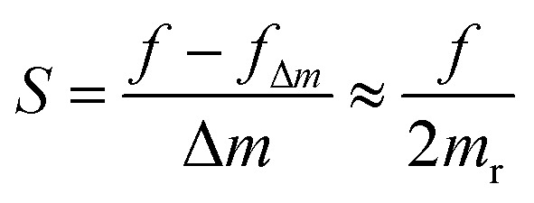
Mechanical resonance is a non-linear response of an oscillating system to specific frequencies linking the external stimuli and the intrinsic microstructure and elastic properties of a material. Resonators are widely used as sensors in micro-/nanoelectromechanical systems (MEMS and NEMS), and are also employed for the elastic property measurements of resonating materials.1–5 While using as mass, chemical and bio-sensors,2–4,6–10 the sensitivity (S) of a resonator is defined by a shift of the resonant frequency with a change of its mass (Δm) calculated as:11,12
 |
1 |
where f and fΔm are the resonant frequencies without and with the mass changes, and mr is the resonator’s mass. When Δm ≪ mr, sensitivity is approximately equal to the resonant frequency divided by twice the resonator’s mass. Eqn (1) implies that higher sensitivity can be achieved by increasing the resonant frequency or by reducing the resonator’s mass, i.e., downscaling the resonator size. Since the frequency is higher for higher resonance orders, increasing the order of the resonant mode provides a way for increasing the resonator’s sensitivity.11,12 For example, Ghatkesar et al. reported that the mass sensitivity is linearly proportional to the square of the mode order.11 Moreover, the resonant response to the driving frequency, defined as a quality factor, is also enhanced with increasing mode order.13,14 These facts clearly point at the significance of high-order and high frequency nanoscale resonators for NEMS. However, it is still challenging to realize high-order resonances at high frequencies due to the large energy dissipation and strict resonant conditions.15,16 By using the top-down approach, high-order normal and parametric resonances were demonstrated,17,18 with a resonant frequency of several MHz.17 Bottom-up grown nanowires (NWs) are attractive as high frequency resonators because of their high crystallinity and small mass. A high frequency, ∼200 MHz, of doubly clamped silicon nanowire (Si NW) resonators was reported;19 however, the resonant mode was limited to the 2nd order.20
Silicon is one of the most important materials for MEMS and NEMS because of the availability of high-quality single crystals and compatibility with microfabrication techniques of the semiconductor industry. One of the most fundamental requirements for application of Si NEMS devices is the elastic properties on the nanometer scale. In previous studies, the Young's modulus of Si NWs was reported in a wide range, from 120 to 170 GPa in the [110] direction21–23 and 60 to 210 GPa in the [111] direction.21,24–31 In addition, there is still controversy over the size scaling effects with respect to Si’s elastic modulus.21,23,27,29 Gordon et al. used a resonance method and reported that the elastic modulus increases with decreasing the NW diameter,27 whereas Calahorra et al. reported the opposite trend under a bending test.21 Such a controversy calls for an accurate measurement of the elastic modulus of Si NWs with direct correlation with their microstructures, such as crystallinity, orientation, diameter and oxide layer thickness.
In this work we investigated the mechanical resonance of individual Si NW cantilevers using an in situ transmission electron microscopy (TEM) approach.31 By carefully tuning the frequency of the oscillating electric field acting on the highly crystallized Si NWs, high-order resonances with high frequencies were realized and visualized up to the 5th order of normal and parametric modes at frequencies of ∼137.5 MHz and ∼68.6 MHz, respectively. The frequencies and their ratios for 10 resonant modes were consistent with the predictions of the classical Euler–Bernoulli (E–B) beam theory. In addition, the precision of the resonant frequency was found to be enhanced for higher resonant mode orders, as the deviations reduced from 3.14% for the 1st order to 0.25% for the 5th order. The converging trend of the resonant frequency is attributed to the higher energy dissipation at higher resonant mode orders, based on the calculation and analysis of the input electric energy and the output mechanical energy from direct observation. We applied these highly sensitive cantilevers to evaluate the elastic moduli of Si NWs and the oxide layer effects. The elastic modulus was found to be consistent with that of bulk Si crystals and the length scaling effects were absent down to the 20 nm level.
Experimental
In situ TEM resonance experimental setup for individual Si NWs
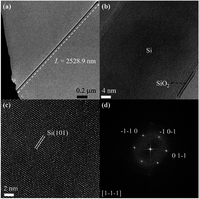
The Si NWs are grown using a vapor–liquid–solid (VLS) approach32 (see also Note S1†). Fig. 1 demonstrates the structural characterization of a typical Si NW by TEM. The length (L) of this Si NW is ∼2529 nm (Fig. 1(a)), which was carefully calibrated by considering the height difference and the TEM magnification, as explained in Note S2.† We used the minimum contrast defocus to estimate the height difference of the two ends. According to the calculated contrast transfer function (CTF), the minimum contrast defocus is about −14 nm. The defocus error should be within 10 nm, and the average error of the length is ∼0.17%, as demonstrated in Note S3.† The circular cross-sectional view of the NW (see Fig. S2†) shows a uniform diameter of ∼23.3 nm and the NW is covered by a naturally formed thin amorphous SiO2 layer (Fig. 1(b)). The high-resolution TEM (HRTEM) image shows that the Si NW has a single-crystalline structure and presents clearly resolved lattice fringes of Si (101) planes (Fig. 1(c)). The corresponding fast Fourier transform (FTT) pattern (Fig. 1(d)) is indexed as the Si [1−1−1] zone axis, with the NW growth direction along the [101] orientation.
Fig. 1. TEM characterization of a Si NW. (a) The Si NW’s length (L) was measured under careful calibration of the tilt angle and TEM magnification. (b) The high magnification TEM image shows a thin silicon oxide (SiO2) layer on the surface. (c) The high-resolution TEM (HRTEM) image demonstrates a single crystalline structure revealing clearly resolved Si (101) lattice fringes. (d) The fast Fourier transform (FFT) pattern can be indexed as the [1−1−1] zone axis, and the growth direction is along the [101] orientation.
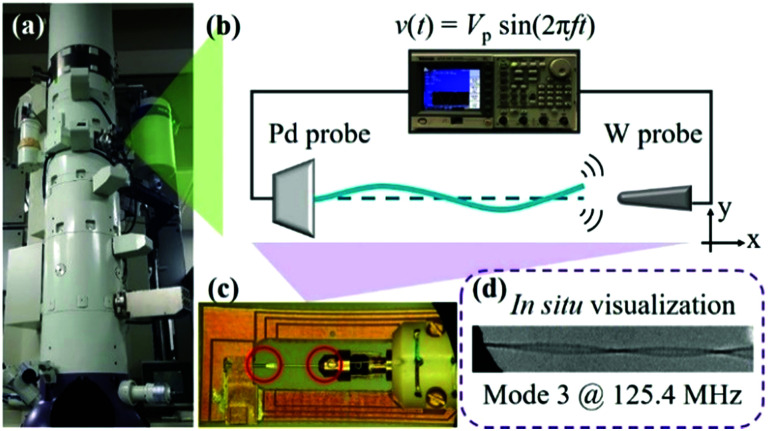
The mechanical vibration of a Si NW is induced by an oscillating electric field between the Si NW and a W probe (see probe preparation in Note S4†) in a JEOL-3100F TEM shown in Fig. 2, as explained in Note S5.† Based on the Euler–Bernoulli (E–B) beam theory, the equation of motion for a uniform circular cross-sectional NW is derived as:33
 |
2 |
where ρ is the density, A(x) is the cross-sectional area, u(x,t) is the displacement of the NW in the lateral direction, Eeff is the effective elastic modulus, and I is the area moment of inertia (I = πD4/64, where D is the diameter) of the Si NW, and F (x,t) is the external force, which equals to Fe in eqn (S2).† For a free vibration: F(x,t) = 0, the solution for the normal mode resonant frequency is:
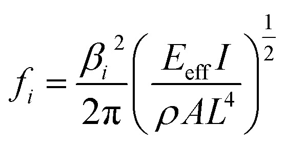 |
3 |
where i is the mode order (i ≥ 1), fi is the resonant frequency at ith order, and L is the length of the NW. In our experiment, the resonant condition for the fixed–free boundary is given by: cos βiL·cosh βiL = −1, with eigenvalues β1 = 1.87, β2 = 4.69, β3 = 7.85, β4 = 10.99 and βi ≈ (2i − 1)π/2 for i ≥ 5. In addition to the normal mode resonance, parametric modes could be found at frequencies 2fi/n for the nth parametric modes, by solving eqn (2) with a non-zero periodic force, as explained in Note S6.†
Fig. 2. Experimental setup for in situ TEM resonance observation. (a) A photograph of the JEOL-3100F TEM operated at 300 kV. (b) An arbitrary function generator (AFG3152C) provides a sinusoidal signal v(t) = Vp sin(2πfdt), where Vp is the amplitude of the peak voltage and fd is the driving frequency. A piezo-controlled tungsten (W) probe is located on the right side. On the left side, individual Si NWs are attached to a flattened palladium (Pd) edge. (c) A photograph of the STM-TEM holder with a fixed Pd electrode and a piezo-controlled W probe as marked with red circles. (d) An example of a Si NW oscillating at the 3rd order.
Results and discussion
Realization and observation of five normal and parametric resonances
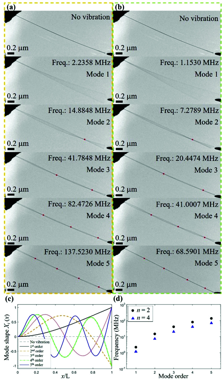
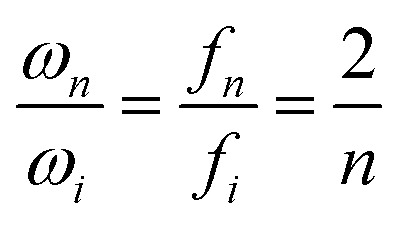
In order to measure the resonant frequency at different mode orders, we first swept the driving frequency within a certain frequency range, as predicted by eqn (3) from the NW’s dimensions. Then, we finely tuned the driving frequency to induce the largest vibration amplitude to locate the resonant frequency. Under careful tuning, we were able to realize and observe up to 10 resonant mode orders for one Si NW. Fig. 3(a) and Video S1† demonstrate the in situ recorded mechanical resonant motions, from the 1st order to the 5th order, at the resonant frequencies of ∼2.2 MHz, ∼14.9 MHz, ∼41.8 MHz, ∼82.5 MHz and ∼137.5 MHz. Another series of resonant frequencies, from the 1st order to the 5th order (Fig. 3(b)), were recorded and could be denoted as the parametric resonance. The relation between normal and parametric resonances can be derived by the Mathieu equation (see eqn S(3)†). In the Strutt diagram34 (see Fig. S4†), the orange shaded area illustrates the instability regions, where the parametric resonance can be excited, as described in Note S6,† with the resonant frequency written as:34–36
 |
4 |
where ωn and fn = ωn/2π are the parametric angular frequency and frequency, n is the parametric mode (n = 1, 2, …), and ωi and fi = ωi/2π are the normal mode angular frequency and frequency. To clarify the notation of different orders at different parametric modes, n denotes the parametric modes, with n = 2 for normal mode resonance, and n = 4 for the 2nd parametric mode. And i represents the resonance orders at the same parametric mode, from the 1st order to the 5th order, for both normal and 2nd parametric modes. Simulated resonating shapes up to the 5th order from the E–B beam theory are presented in Fig. 3(c). More details for different resonating Si NWs at different modes are provided in Fig. S5–S6.† It is worth mentioning that the resonant frequency of the 4th order at n = 4 is close to the resonant frequency of the 3rd order at n = 2. In situ TEM observations and measurements have the advantage of directly recording the shape of the resonating NW to unambiguously identify the resonant mode and order. The ratios of node intervals from the TEM images of the resonating shapes are well consistent with the theoretically calculated values as listed in Table S2.† The resonant frequencies are plotted against the resonance orders for both normal and parametric modes (Fig. 3(d)), where black solid circles mark the normal mode at ωi (n = 2) and blue triangles represent the parametric mode at ωi/2 (n = 4). The ratios of frequencies between the two modes are calculated to be close to βi2/βj2 (Fig. S7†), where j denotes the mode order, consistent with the prediction from eqn (3). The ratio between two parametric resonances is described in eqn (4). The ratio of ω4/ω2 is plotted in Fig. S8;† revealing a good agreement with the theoretically predicted value of 0.5. It is found that the deviations are reduced from 3.14% to 0.25% for the 1st and 5th orders, respectively.
Fig. 3. Normal and parametric resonances of a Si NW observed by in situ TEM. (a) Normal mode (n = 2) resonant motions from the 1st order to the 5th order at ∼2.2 MHz, ∼14.9 MHz, ∼41.8 MHz, ∼82.5 MHz and ∼137.5 MHz. Node positions are marked by red solid circles. (b) Parametric resonance (n = 4) from the 1st order to the 5th order at ∼1.1 MHz, ∼7.2 MHz, ∼20.4 MHz, ∼41.0 MHz and ∼68.6 MHz. (c) Simulated resonant shapes from the 1st order to the 5th order. (d) Plot of resonant frequencies of normal and parametric resonances (n = 2 and 4) from the 1st order to the 5th order.
It is noticed that the lower resonance orders could be excited in a wider frequency range compared to the higher orders. For example, for the 1st order, a 10 kHz sweeping step can easily locate the resonance. However, for the 5th order, the step needs to be 100 Hz, which is ∼1 ppm of a resonant frequency of ∼100 MHz. Such a converging trend for the resonance conditions could be understood from the analysis of the input, output and dissipated energies. In previous studies, energy dissipation has been attributed to environmental factors, such as viscosity, temperature, clamping loss, intrinsic defects, and the change of the elastic energy.11,15,16,37–42 Here, we take advantage of the in situ technique to directly measure and calculate the input and output energies. The input energy can be assumed as the energy of a capacitor, between the free end of the Si NW and the W probe.30,43 The energy stored in the capacitor (Wc) is expressed as:
 |
5 |
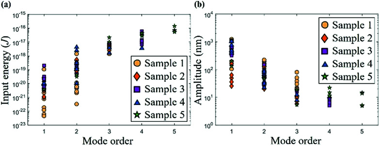
where ε0 is the vacuum permittivity, d is the gap between the Si NW and W probe, V is the applied voltage, V = Vdc + Vp, and ASi and AW (AW = ηASi) are the apex areas of the Si NW and W probe, where η is a geometric factor. The input energy and measured vibration amplitude at different mode orders are illustrated in Fig. 4. According to our calculations (see Note S8†), the potential energy stored in the oscillating Si NW increases with increasing mode order, assuming the same vibration amplitude. The energy dissipation is predicted to increase with the resonant modes, when comparing the energy difference between the input and output energies (see Note S9†). This indicates that higher input energy is needed, and stricter conditions are required to induce high-order modes. It should be emphasized that previously only the 2nd order was observed for Si NW resonators.20 In Note S10,† the intrinsic and extrinsic limits for observing high resonant mode order have been analysed. For the first time, our work demonstrates that up to the 5th order of normal and parametric resonances could be realized and directly observed by in situ TEM.
Fig. 4. Input energy and measured vibration amplitude at different resonant mode orders. (a) Input energy for five Si NW samples. Higher input energy and more strict resonant conditions are required for higher mode orders. (b) The measured vibration amplitudes decrease with the mode order, indicating higher energy dissipation and more strict resonant conditions for higher orders.
Evaluation of the Si NW’s modulus and absence of size-effects
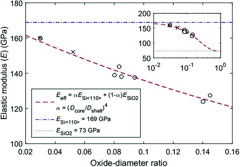
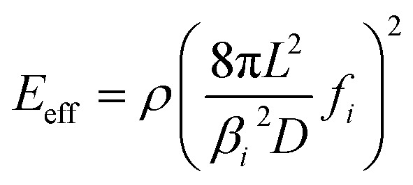
The strict resonant requirement at high-order modes provides an opportunity to precisely evaluate the elastic modulus of Si NWs. By calculations from eqn (3) using the frequencies of the 2nd resonance order, it is found that the effective modulus of the NW is in the range between ∼124 GPa and ∼160 GPa (Fig. 5), depending on the thickness of the oxide layer. The HRTEM image (Fig. 1(c)) reveals that the Si NW grows along the [110] direction and its surface is covered by a thin SiO2 layer. Therefore, the Si NW can be modelled as a core–shell structure, where the bulk Si〈110〉 NW serves as the core and the SiO2 layer as the shell. The elastic modulus of the core–shell structure (Ecs) can be calculated using the flexural rigidity model:27
| Ecs = αEcore + (1 − α)Eshell | 6 |
where Ecore is the Young's modulus of bulk Si along the [110] direction and Eshell is the modulus of SiO2 (ESiO2). α = (Dcore/Dshell)4, where Dcore is the diameter of core Si and Dshell is the diameter of the whole Si NW; the SiO2 layer thickness is equal to (Dshell − Dcore)/2. Ecs is equal to Eeff of the Si NW derived using eqn (3) as:
 |
7 |
Fig. 5. Elastic moduli predicted from the core–shell model and experimentally measured results. Circles are calculated by considering the normal mode (n = 2), and crosses are derived using the parametric mode (n = 4). The inset presents the full range modelling from pure Si〈110〉 to pure SiO2 of the core–shell NW. Blue dashed and green dotted lines represent the moduli of bulk Si〈110〉 and SiO2, respectively.
To be noticed, a nanoparticle has been observed attached on the free-end of the Si NW (Fig. 1(a)). The nanoparticle is the gold particle used as the catalyst in VLS growth, which can be considered as an added mass to cause a shift in the resonant frequency of ∼2%; and an error in the Eeff of ∼0.77%, as calculated in Note S11.† Here, we defined an oxide–diameter ratio as the thickness of the SiO2 layer divided by the diameter (D) of the Si NW. The model predicts an oxide–diameter ratio ranging from ∼0.02 to ∼0.15 (Fig. 5), and offers a full range simulation (Fig. 5 inset) under the combination of ESi〈110〉 (∼169 GPa),44ESiO2 (∼73 GPa)45 and α. Comparing the experimental data of the 2nd order with the flexural rigidity model (Fig. 5), the coefficient of determination (R2) is 0.97, which indicates that the model provides a reliable description of the experimental data for a diameter (Dcore) ranging from ∼19 nm to ∼33 nm. Importantly, the Si NW displays no size-effects within this diameter range, and the modulus is consistent with that of the bulk crystals, confirming the validity of the classical continuum mechanics at the NW sizes down to ∼20 nm.
Elasticity and size-effects of Si NWs have been intensively investigated, and controversial results have been reported, and the feasibility of continuum mechanics is also controversial.21,23,29,46 For example, Zhu et al. applied tensile tests to measure the mechanical properties of Si NWs and demonstrated that the Young's modulus decreases upon reducing the size of the NWs.23 There are two models, one is the continuum model on the macroscale and the other is the atomic model. In the continuum system, the NW is considered as a homogeneous and linear elastic material; in the atomic model, the nature of the individual bonding interactions presents the mechanical properties of an oscillating chain of atoms. According to the literature,47,48 molecular dynamics (MD) simulations and first principles calculations were used to simulate the elastic modulus of the Si NWs. Surface effects, such as surface elasticity and bonding on the NW’s surface, have been addressed as the main factors of size-effects. The surface area to volume ratio (RS) is a parameter used to evaluate size-effects (RS = 4a/D where a is the interatomic distance, approximately 0.2 nm). Numerical results show that when RS is smaller than ∼8%,48 the surface effects show minor contribution to the elastic modulus. In our work, RS is estimated to be ∼4%, with the smallest diameter being ∼20 nm. In addition, the surface of the Si NWs is covered by an oxide layer, which saturates the dangling bonds of the Si surface. Because of the small proportion of surface atoms and surface saturation it is reasonable that size-effects are absent down to the 20 nm level. We have analysed the different size scaling behaviours from three aspects, by comparing our work with Zhu et al.'s paper23 as an example. First, different experimental methods have been used. We used the resonance method and previous work used the tensile elongation method. Second, different models have been considered. We have considered the effect of the surface oxide layer by using a core–shell model, instead of the oxide layer-free model in previous work. Third, the size range is different. The size related softening effects were reported to be strong in the sub-20 nm region, and the minimum diameter in our work is ∼20 nm.
Comparison of resonant frequency and mode orders of Si resonators
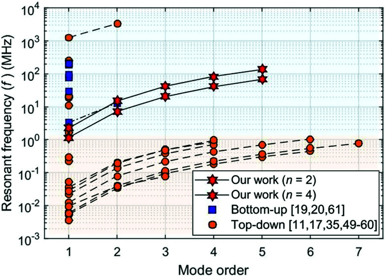
As discussed in the Introduction, the sensitivity of mechanical resonators is related to the resonant frequency, mode order and oscillator’s mass. Fig. 6 presents a plot of the resonant frequency and the mode order of micro/nano-Si resonators fabricated using a top-down approach11,17,35,49–60 compared to nano-Si resonators made using a bottom-up approach.19,20,61 Generally, top-down Si micro/nano-resonators can demonstrate very high resonant mode orders at low frequencies due to the micrometer size.11,17,52,59 To enhance the frequency and reduce the mass of the resonators, NW resonators have been intensively investigated during the past two decades. Indeed, very high frequency resonators, at approximately 200 MHz, have been demonstrated.19 However, up to now, only the 1st and the 2nd orders of normal mode resonances have been realized in NW resonators.20 By contrast, in the current work, the full potential of Si NW resonators has been demonstrated by in situ TEM measurements and direct observations. Normal and parametric resonances up to the 5th order were realized and directly observed at frequencies of ∼100 MHz level.
Fig. 6. Comparison of the resonant frequency and the mode order of Si resonators. The square and circle marks represent the results from the bottom-up and top-down approaches, respectively. Si NW resonators in the current work (red stars) demonstrate the high-order and high frequency working regime.
Conclusions
By using an in situ TEM method, we realized and directly observed both normal and parametric modes of Si NW resonators, up to the 5th order, at the resonant frequencies of ∼100 MHz. The frequencies and ratios of different mode orders and parametric resonances were consistent with the prediction of the classical Euler–Bernoulli beam theory and the parametric resonance derived by the Mathieu equation, implying that the continuum model is valid down to the nanometer scale. The resonating ranges demonstrated a converging trend with increasing mode orders and resonant frequencies, implying the potential applications for precise sensors at high-order resonant modes. The elastic moduli of the Si NWs have been accurately evaluated, and no size-effects were found for the NW diameter down to 20 nm.
Conflicts of interest
There are no conflicts to declare.
Supplementary Material
Acknowledgments
The work was supported by JSPS Kakenhi Grant 25820336, the Transmission Electron Microscopy Station, World Premier International (WPI) Center for Materials Nanoarchitectonics (MANA), National Institute for Materials Science (NIMS), Japan, National Cheng Kung University (NCKU), Ministry of Science and Technology of Taiwan (MOST-105-2218-E-006-016-MY2 and MOST-107-2634-F-006-009), and MOST AI Biomedical Research Center at NCKU. F.-C. H. acknowledges the scholarships from the NIMS internship program and Global Networking Talent 3.0 Plan – Biomedical Engineering sponsored by the Medical Device Innovation Center at NCKU and the Ministry of Education, Taiwan. D. G. is grateful to the Australian Research Council (ARC) for granting a Laureate Fellowship FL160100089 and QUT Project No. 322170-0355/51.
Electronic supplementary information (ESI) available. See DOI: 10.1039/c8na00373d
Notes and references
- Bunch J. S. van der Zande A. M. Verbridge S. S. Frank I. W. Tanenbaum D. M. Parpia J. M. Craighead H. G. McEuen P. L. Science. 2007;315:490–493. doi: 10.1126/science.1136836. [DOI] [PubMed] [Google Scholar]
- Resonant MEMS, ed. O.Brand, I.Dufour, S. M.Heinrich and F.Josse, Wiley-VCH Verlag GmbH & Co. KGaA, Weinheim, Germany, 2015 [Google Scholar]
- Ekinci K. L. Roukes M. L. Rev. Sci. Instrum. 2005;76:061101. doi: 10.1063/1.1927327. [DOI] [Google Scholar]
- Craighead H. G. Science. 2000;290:1532–1535. doi: 10.1126/science.290.5496.1532. [DOI] [PubMed] [Google Scholar]
- Jensen K. Weldon J. Garcia H. Zettl A. Nano Lett. 2007;7:3508–3511. doi: 10.1021/nl0721113. [DOI] [PubMed] [Google Scholar]
- Burg T. P. Godin M. Knudsen S. M. Shen W. Carlson G. Foster J. S. Babcock K. Manalis S. R. Nature. 2007;446:1066–1069. doi: 10.1038/nature05741. [DOI] [PubMed] [Google Scholar]
- Calleja M. Nordström M. Álvarez M. Tamayo J. Lechuga L. M. Boisen A. Ultramicroscopy. 2005;105:215–222. doi: 10.1016/j.ultramic.2005.06.039. [DOI] [PubMed] [Google Scholar]
- Jensen K. Kim K. Zettl A. Nat. Nanotechnol. 2008;3:533–537. doi: 10.1038/nnano.2008.200. [DOI] [PubMed] [Google Scholar]
- Poncharal P. Science. 1999;283:1513–1516. doi: 10.1126/science.283.5407.1513. [DOI] [PubMed] [Google Scholar]
- Yang Y. T. Callegari C. Feng X. L. Ekinci K. L. Roukes M. L. Nano Lett. 2006;6:583–586. doi: 10.1021/nl052134m. [DOI] [PubMed] [Google Scholar]
- Ghatkesar M. K. Barwich V. Braun T. Ramseyer J.-P. Gerber C. Hegner M. Lang H. P. Drechsler U. Despont M. Nanotechnology. 2007;18:445502. doi: 10.1088/0957-4484/18/44/445502. [DOI] [Google Scholar]
- Braun T. Barwich V. Ghatkesar M. K. Bredekamp A. H. Gerber C. Hegner M. Lang H. P. Phys. Rev. E: Stat., Nonlinear, Soft Matter Phys. 2005;72:031907. doi: 10.1103/PhysRevE.72.031907. [DOI] [PubMed] [Google Scholar]
- Van Eysden C. A. Sader J. E. J. Appl. Phys. 2007;101:044908. doi: 10.1063/1.2654274. [DOI] [Google Scholar]
- Biedermann L. B. Tung R. C. Raman A. Reifenberger R. G. Yazdanpanah M. M. Cohn R. W. Nanotechnology. 2010;21:305701. doi: 10.1088/0957-4484/21/30/305701. [DOI] [PubMed] [Google Scholar]
- Ko J. H. Jeong J. Choi J. Cho M. Appl. Phys. Lett. 2011;98:171909. doi: 10.1063/1.3575560. [DOI] [Google Scholar]
- Sader J. E. Lee J. Manalis S. R. J. Appl. Phys. 2010;108:114507. doi: 10.1063/1.3514100. [DOI] [PMC free article] [PubMed] [Google Scholar]
- Killgore J. P. Hurley D. C. Nanotechnology. 2012;23:055702. doi: 10.1088/0957-4484/23/5/055702. [DOI] [PubMed] [Google Scholar]
- Jia Y. Du S. Arroyo E. Seshia A. A. Appl. Phys. Lett. 2018;112:171901. doi: 10.1063/1.5024667. [DOI] [Google Scholar]
- Feng X. L. He R. Yang P. Roukes M. L. Nano Lett. 2007;7:1953–1959. doi: 10.1021/nl0706695. [DOI] [Google Scholar]
- Malvar O. Gil-Santos E. Ruz J. J. Ramos D. Pini V. Fernandez-Regulez M. Calleja M. Tamayo J. San Paulo A. Appl. Phys. Lett. 2013;103:033101. doi: 10.1063/1.4813819. [DOI] [Google Scholar]
- Calahorra Y. Shtempluck O. Kotchetkov V. Yaish Y. E. Nano Lett. 2015;15:2945–2950. doi: 10.1021/nl5047939. [DOI] [PubMed] [Google Scholar]
- Zhang H. Tersoff J. Xu S. Chen H. Zhang Q. Zhang K. Yang Y. Lee C.-S. Tu K.-N. Li J. Lu Y. Sci. Adv. 2016;2:e1501382. doi: 10.1126/sciadv.1501382. [DOI] [PMC free article] [PubMed] [Google Scholar]
- Zhu Y. Xu F. Qin Q. Fung W. Y. Lu W. Nano Lett. 2009;9:3934–3939. doi: 10.1021/nl902132w. [DOI] [PubMed] [Google Scholar]
- Hsin C.-L. Mai W. Gu Y. Gao Y. Huang C.-T. Liu Y. Chen L.-J. Wang Z.-L. Adv. Mater. 2008;20:3919–3923. doi: 10.1002/adma.200800485. [DOI] [Google Scholar]
- Zhang K. Zhu Q. Chen Z. Sensors. 2017;17:1621. doi: 10.3390/s17071621. [DOI] [PMC free article] [PubMed] [Google Scholar]
- San Paulo A. Bokor J. Howe R. T. He R. Yang P. Gao D. Carraro C. Maboudian R. Appl. Phys. Lett. 2005;87:053111. doi: 10.1063/1.2008364. [DOI] [Google Scholar]
- Gordon M. J. Baron T. Dhalluin F. Gentile P. Ferret P. Nano Lett. 2009;9:525–529. doi: 10.1021/nl802556d. [DOI] [PubMed] [Google Scholar]
- Tabib-Azar M. Nassirou M. Wang R. Sharma S. Kamins T. I. Islam M. S. Williams R. S. Appl. Phys. Lett. 2005;87:113102. doi: 10.1063/1.2042549. [DOI] [Google Scholar]
- Sohn Y.-S. Park J. Yoon G. Song J. Jee S.-W. Lee J.-H. Na S. Kwon T. Eom K. Nanoscale Res. Lett. 2010;5:211–216. doi: 10.1007/s11671-009-9467-7. [DOI] [PMC free article] [PubMed] [Google Scholar]
- Garcia-Sanchez D. San Paulo A. Esplandiu M. J. Perez-Murano F. Forró L. Aguasca A. Bachtold A. Phys. Rev. Lett. 2007;99:085501. doi: 10.1103/PhysRevLett.99.085501. [DOI] [PubMed] [Google Scholar]
- Tang D.-M. Ren C.-L. Wang M.-S. Wei X. Kawamoto N. Liu C. Bando Y. Mitome M. Fukata N. Golberg D. Nano Lett. 2012;12:1898–1904. doi: 10.1021/nl204282y. [DOI] [PubMed] [Google Scholar]
- Fukata N. Mitome M. Sekiguchi T. Bando Y. Kirkham M. Hong J.-I. Wang Z. L. Snyder R. L. ACS Nano. 2012;6:8887–8895. doi: 10.1021/nn302881w. [DOI] [PubMed] [Google Scholar]
- Rao S. S. and Yap F. F., Mechanical Vibrations, Prentice Hall Upper; Saddle River, 2011, vol. 4 [Google Scholar]
- Nayfeh A. H. and Mook D. T., Nonlinear Oscillations, John Wiley & Sons, 2008 [Google Scholar]
- Turner K. L. Miller S. A. Hartwell P. G. MacDonald N. C. Strogatz S. H. Adams S. G. Nature. 1998;396:149–152. doi: 10.1038/24122. [DOI] [Google Scholar]
- Yu M.-F. Wagner G. J. Ruoff R. S. Dyer M. J. Phys. Rev. B: Condens. Matter Mater. Phys. 2002;66:073406. doi: 10.1103/PhysRevB.66.073406. [DOI] [Google Scholar]
- Verbridge S. S. Shapiro D. F. Craighead H. G. Parpia J. M. Nano Lett. 2007;7:1728–1735. doi: 10.1021/nl070716t. [DOI] [PubMed] [Google Scholar]
- Burg T. P. Sader J. E. Manalis S. R. Phys. Rev. Lett. 2009;102:228103. doi: 10.1103/PhysRevLett.102.228103. [DOI] [PubMed] [Google Scholar]
- Harrington D. A. Mohanty P. Roukes M. L. Phys. B. 2000;284–288:2145–2146. doi: 10.1016/S0921-4526(99)02998-1. [DOI] [Google Scholar]
- Schmid S. Hierold C. J. Appl. Phys. 2008;104:093516. doi: 10.1063/1.3008032. [DOI] [Google Scholar]
- Unterreithmeier Q. P. Faust T. Kotthaus J. P. Phys. Rev. Lett. 2010;105:027205. doi: 10.1103/PhysRevLett.105.027205. [DOI] [PubMed] [Google Scholar]
- Imboden M. Mohanty P. Phys. Rep. 2014;534:89–146. doi: 10.1016/j.physrep.2013.09.003. [DOI] [Google Scholar]
- Perisanu S. Gouttenoire V. Vincent P. Ayari A. Choueib M. Bechelany M. Cornu D. Purcell S. T. Phys. Rev. B. 2008;77:165434. doi: 10.1103/PhysRevB.77.165434. [DOI] [PubMed] [Google Scholar]
- Hopcroft M. A. Nix W. D. Kenny T. W. J. Microelectromech. Syst. 2010;19:229–238. [Google Scholar]
- Ni H. Li X. Gao H. Appl. Phys. Lett. 2006;88:043108. doi: 10.1063/1.2165275. [DOI] [Google Scholar]
- Gordon M. J. Baron T. Dhalluin F. Gentile P. Ferret P. Nano Lett. 2009;9:525–529. doi: 10.1021/nl802556d. [DOI] [PubMed] [Google Scholar]
- Pishkenari H. N. Afsharmanesh B. Akbari E. Curr. Appl. Phys. 2015;15:1389–1396. doi: 10.1016/j.cap.2015.08.002. [DOI] [Google Scholar]
- Rudd R. E. Lee B. Mol. Simul. 2008;34:1–8. doi: 10.1080/08927020701730435. [DOI] [Google Scholar]
- Labuda A. Kocun M. Lysy M. Walsh T. Meinhold J. Proksch T. Meinhold W. Anderson C. Proksch R. Rev. Sci. Instrum. 2016;87:073705. doi: 10.1063/1.4955122. [DOI] [PubMed] [Google Scholar]
- Jiang W. C. Lu X. Zhang J. Lin Q. Opt. Express. 2012;20:15991. doi: 10.1364/OE.20.015991. [DOI] [PubMed] [Google Scholar]
- Yang J. Ono T. Esashi M. J. Microelectromech. Syst. 2002;11:775–783. doi: 10.1109/JMEMS.2002.805208. [DOI] [Google Scholar]
- Gates R. S. Osborn W. A. Pratt J. R. Nanotechnology. 2013;24:255706. doi: 10.1088/0957-4484/24/25/255706. [DOI] [PubMed] [Google Scholar]
- Bargatin I. Myers E. B. Aldridge J. S. Marcoux C. Brianceau P. Duraffourg L. Colinet E. Hentz S. Andreucci P. Roukes M. L. Nano Lett. 2012;12:1269–1274. doi: 10.1021/nl2037479. [DOI] [PMC free article] [PubMed] [Google Scholar]
- Carr D. W. Evoy S. Sekaric L. Craighead H. G. Parpia J. M. Appl. Phys. Lett. 1999;75:920–922. doi: 10.1063/1.124554. [DOI] [Google Scholar]
- Nasr Esfahani M. Kilinc Y. Çagatay Karakan M. Orhan E. Hanay M. S. Leblebici Y. Erdem Alaca B. J. Micromech. Microeng. 2018;28:045006. doi: 10.1088/1361-6439/aaab2f. [DOI] [Google Scholar]
- Koumela A. Mercier D. Gouttenoire V. Marcoux C. Purcell S. T. Duraffourg L. Procedia Eng. 2011;25:1649–1652. doi: 10.1016/j.proeng.2011.12.408. [DOI] [Google Scholar]
- Li X. Ono T. Wang Y. Esashi M. Appl. Phys. Lett. 2003;83:3081–3083. doi: 10.1063/1.1618369. [DOI] [Google Scholar]
- Tsushima T. Asahi Y. Tanigawa H. Furutsuka T. Suzuki K. Jpn. J. Appl. Phys. 2018;57:067201. doi: 10.7567/JJAP.57.067201. [DOI] [Google Scholar]
- Ikehara T. Lu J. Konno M. Maeda R. Mihara T. J. Micromech. Microeng. 2007;17:2491–2494. doi: 10.1088/0960-1317/17/12/015. [DOI] [Google Scholar]
- Li M. Pernice W. H. P. Tang H. X. Nat. Nanotechnol. 2009;4:377–382. doi: 10.1038/nnano.2009.92. [DOI] [PubMed] [Google Scholar]
- He R. Feng X. L. Roukes M. L. Yang P. Nano Lett. 2008;8:1756–1761. doi: 10.1021/nl801071w. [DOI] [PubMed] [Google Scholar]
Associated Data
This section collects any data citations, data availability statements, or supplementary materials included in this article.


