Abstract
Here, we have investigated some mixed metal hybrid halide perovskite materials by employing first principle calculation method. In this regard we have designed some Sn and Ge based hybrid halide (iodide) perovskite materials incorporating dimethylammonium (DMA) organic cation and studied their structural, optoelectronic and photovoltaic properties. Observed tolerance factor (TF) and dihedral factor (μ) manifests that our studied compounds form stable three dimensional perovskite structure. Additionally, the observed negative value of formation energy indicates their thermodynamic stability. Calculated band gap values indicate the semiconducting nature of the compounds. We have also calculated the real and imaginary part of dielectric function as well as absorption coefficient of all the studied compounds. Our investigation reveals that compounds with equal amount of Sn and Ge content exhibit higher value of dielectric function and absorption coefficient among the studied compounds. Study of photovoltaic performances reveal that DMASn0.75Ge0.25I3 exhibits the highest value of theoretical power conversion efficiency (PCE) i.e., 17.42% among the studied compounds. This investigation will help researchers to design Pb-free hybrid perovskite materials which will be beneficial for the world.
Here, we have investigated some mixed metal hybrid halide perovskite materials by employing first principle calculation method.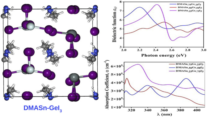
1. Introduction
Perovskite based optoelectronic devices have gain attention over the conventional Si-based devices due to their low weight, mechanical flexibility, low fabrication cost, tunable band gaps etc. These materials are widely used in the field of photovoltaics such as solar cells, organic light emitting diodes (OLED), organic field effect transistors etc.1–3 It has already been reported that the use of hybrid halide perovskite based semiconducting materials in photovoltaics leads to PCE up to 25.5%.4–7 The chemical formula of the perovskite structure is ABX3, where A site is usually occupied by a monovalent organic cation viz. methylammonium (MA), dimethylammonium (DMA), formamidinium (FA) etc., B site is occupied by a divalent metal cation viz. Pb2+, Sn2+ or Ge2+ and X site is occupied by halide anions viz. Cl−, Br− or I−.8 Lead halide perovskites have turned up as a class of highly optimistic materials for photovoltaic applications in the last 10 years due to their excellent optoelectronic properties.8–10 Besides the high PCE of Pb based perovskites the commercialization of these materials are still a big challenge due to their poor stability and toxicity toward environment.9–12 The crystal structure of organic–inorganic hybrid halide perovskites (OIHP) are found to be very responsive to temperature. It has already been reported in literature that OIHPs viz. CH3NH3PbX3 forms cubic structure at high temperature. At low temperature this material becomes tetragonal and then further it forms orthorhombic crystal structure.13–15 The A, B and X sites of ABX3 can be altered or tuned to improve the efficiency of perovskite-based photovoltaic materials.
Now a days, researchers are trying to replace the lead content by some environment friendly elements viz. Sn, Ge and some transition metals etc. As per literature, the substitution of Pb with Sn, Ge, Cu, Zn etc. show signficant improvement in the efficiency of the perovskite based photovoltaics.16 Besides, the addition of Zn2+ in perovskite-based photovoltaics improve the regular PCE from 12.1% to 16.3%.16 Moreover, we have also achieved a PCE value of 20.13% for Sn based hybrid halide perovskite material in our previous work.17
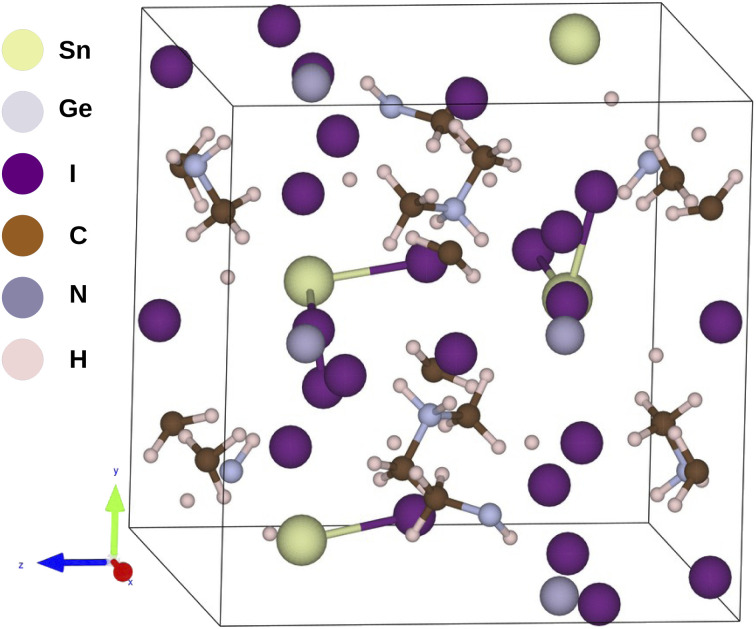
In this work we have theoretically investigated Sn, Ge and mixed Sn and Ge based hybrid halide (iodide) perovskites incorporated with dimethylammonium i.e., (CH3)2NH2+ (DMA) organic cation. We have obtained the crystallographic information files (CIF) of our studied compounds from the crystallography open database and Materials Project which are free databases for crystal structures.18–20 The parent framework of the investigated compounds are provided in Fig. 1 and their optimized coordinates are provided in Table S1 in ESI.† In this regard we have mixed Sn and Ge in different proportions and investigated their structural, electronic, optical and photovoltaic properties by employing DFT formalism embodied in the Quantum Espresso program package. The reason for choosing DMA as organic cation for our investigation is due to its suitable size to fit into the octahedral voids of the perovskite crystal and also it exhibits similar electronic properties with methyl ammonium (MA) cation which has been widely studied in recent times. However, we have considered only I− ion for our studied perovskite materials owing to its excellent optoelectronic properties observed in our previous work.17 To investigate the structural and thermodynamic stability of our studied compounds we have calculated tolerance factor (TF), octahedral factor (μ) and formation energy (ΔE) respectively. To study the electronic properties of our studied compounds we have calculated band gaps and density of states for all the studied compounds. To further evaluate the optical properties and photovoltaic performances of our studied compounds we have calculated real and imaginary part of dielectric function, absorption coefficient, open circuit voltage (Voc), short circuit current density (Jsc) and theoretical PCE (η) respectively for all the compounds.
Fig. 1. Sketch of the optimized structure of DMASn0.50Ge0.50I3.
2. Computational methodology and its validation
We have carried out our calculations by employing first principle method within the framework of density functional theory (DFT) using the plane wave pseudopotential approach (PWSCF) embodied in Quantum Espresso (QE) code.21–23 The crystallographic information file of DMASnI3 (space group Pna21) have been obtained from materials project.18–20 We have carried out the initial calculations using two different exchange correlation functionals viz. Perdew–Burke–Ernzerhof functional (PBE) and Perdew Burke Ernzerhof for solids (PBEsol) and the convergence in case of plane wave cut-off, lattice parameters as well as the charge density cut-off is attained.20–22,24 To validate the adopted methodology that we have employed through out the investigation, we have also carried out test SCF calculation for one reference compound (DMAPbI3; whose lattice parameters and Eg values are already reported) using four different functionals viz. PBE, PBEsol, PBE0 and HSE06 respectively.25,26 The results of our calculation have been presented in Table 1. From Table 1 it is observed that the calculated lattice parameters and band gaps employing PBE functional exhibits better correlation with the experimentally reported parameters. Therefore, to keep the computational cost under control we have performed our all calculations using PBE functional. To evaluate the electronic properties of the studied compounds we have used PBE exchange correlation functional with scalar-relativistic (SR) ultra-soft pseudopotentials (US-PPs) for all elements.27 Further, we have employed Monkhorst–Pack grids 2 × 2 × 2 and 4 × 4 × 2 k-point mesh of the Brillouin zone for geometry optimization.28 The equilibrium lattice parameters for each of the compounds can be obtained by total minimization of energy by employing the conjugate-gradient method. Moreover, the kinetic energy cut-offs for the plane-wave basis set have been optimized in order to confirm the residual forces on atoms converged to below 0.0005 eV Å−1. To acquire correct description of the electronic structure of OIHP compounds we have taken into account the spin orbit coupling (SOC) effect.29,30 To carry out the SOC calculations of band structures we have employed PBE exchange-correlation functional along with fully relativistic pseudopotentials for the Sn and Ge atoms. All our calculations have been carried out with the cut-off energies for plane wave functions and charge densities in the range 47 to 470 Ry. We have used two sets of Monkhorst–Pack grids 4 × 4 × 2 and 4 × 4 × 4 k-point mesh of Brillouin zone for self consistent and density of states calculation respectively.31 We have used high symmetry points in Brillouin zone to carry out the band structure calculation.
Calculated lattice parameters and band gaps of the reference OIHP material.
| Compound | Functionals | Theoretical | Experimental | ||||||
|---|---|---|---|---|---|---|---|---|---|
| a (Å) | b (Å) | c (Å) | E g (eV) | a (Å) | b (Å) | c (Å) | E g (eV) | ||
| DMAPbI3 | PBE | 8.56 | 9.17 | 15.00 | 2.62 | 8.288 | 8.786 | 14.637 | 2.58 |
| PBEsol | 8.56 | 9.16 | 15.03 | 3.29 | |||||
| PBE0 | 8.56 | 9.17 | 15.03 | 4.77 | |||||
| HSE06 | 8.56 | 9.16 | 15.04 | 4.05 | |||||
The excited state calculations have been performed by employing time dependent density functional theory (TD-DFT) formalism embodied in Quantum Espresso program package. We have calculated the real and imaginary part of dielectric functions by employing norm conserving pseudopotentials and investigated their semiconducting properties. We have also calculated the absorption coefficient by using complex dielectric function and investigated their optical absorption properties.32
3. Results and discussion
3.1. Theoretical details
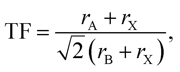
To investigate the structural stability of hybrid perovskites TF and μ values have been calculated by using eqn (1) and (2) respectively33–35 and the values are presented in Table 2.
 |
1 |
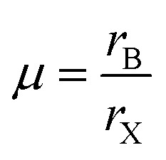
where rA, rB and rX represent the effective ionic radii of the component A, B and X respectively. To get more insight into the structural stability of perovskites we have calculated μ by using eqn (2).36–38
 |
2 |
Tolerance factors (TF) and octahedral factors (μ) of studied compounds.
| Compounds | TF | μ | ΔE (eV) |
|---|---|---|---|
| DMASnI3 | 1.04 | 0.51 | −77.63 |
| DMAGeI3 | 1.17 | 0.35 | −36.54 |
| DMASn0.75Ge0.25I3 | 1.07 | 0.42 | −215.98 |
| DMASn0.50Ge0.50I3 | 1.10 | 0.42 | −170.59 |
| DMASn0.25Ge0.75I3 | 1.14 | 0.57 | −139.64 |
Further, we have calculated the formation energies (ΔE) by using eqn (3) (ref. 20, 39 and 40) and evaluated their thermodynamic stability. The corresponding values are presented in Table 2:
| ΔE = E(ABX3) − E(AX) − E(BX2), | 3 |
where A, B and X represent DMA+, Sn2+/Ge2+ and halide ion (I−) respectively. The negative values of formation energies of ABX3 compounds indicate their easy synthesizability.38
The photovoltaic performance of perovskite systems have been investigated by calculating the parameters, viz. open circuit voltage (Voc), short circuit current density (Jsc) and theoretical PCE (η) based on the band gap values. The Jsc can be calculated by using eqn (4) by estimating that all incident photons will be absorbed, providing, the energies of the studied perovskite materials must be larger than their band gap values,41,42
 |
4 |
where e, E, and S(E) are the electronic charge, the incident photon energy, and the incident spectral power per unit area respectively. To calculate the short-circuit current density of our studied perovskite materials we have used the solar spectrum data provided by the National Renewable Energy Laboratory.33,41,42
Based on the band gap (Eg) and a variable parameter loss-in-potential Eloss of the perovskites, their Voc values can be estimated by using eqn (5),
| Voc = Eg − Eloss, | 5 |
where the Eloss values 0.7 and 0.5 eV are adopted from the literature.33,41,42
The maximum theoretical PCE (η) of hybrid perovskites can be calculated by using the values of Jsc and Voc. The η can be calculated by using eqn (6),
 |
6 |
where FF is the fill factor and Psun is the total incident power and can be calculated by using eqn (7),33,41
 |
7 |
3.2. Phase stability
We have carried out geometry optimization of our studied compounds by employing first principle method. The optimized geometrical parameters of the studied compounds are reported in Table S3 (in the ESI†) and the sketch of the one of our studied compounds (periodic unit cell) is presented in Fig. 1. It is clear from Table S3† that theoretical lattice parameters of DMASnI3 closely resemble to the experimentally reported values. Hence we can draw conclusion that our studied compounds are in orthorhombic crystal phase. In order to evaluate the crystallographic stability of our studied OIHPs we have calculated Goldschmidt tolerance factor (TF) and octahedral factor (μ) for all the studied compounds by using eqn (1) and (2). In this regard we have considered the Shannon ionic radii for Sn2+, Ge2+, I− and DMA+ ions as 1.12, 0.73, 2.20 and 2.73 Å respectively for calculating TF and μ values.33–35,37 It has been already reported that 3D perovskite structures are formed when the value of TF lies within 0.76 < TF < 1.13.36 However, TF alone is not sufficient parameter to explain the stability of hybrid perovskites. Another parameter taken into consideration to depict stability of perovskite structure is the octahedral factor (μ) obtained by eqn (2). μ gives information about the size of B site cations to be coordinated by six anions so that it fits into the octahedral hole.36,37 It has been reported that the metal halide perovskites are found to be stable when μ value lies in the range 0.442 < μ < 0.895.38 The calculated TF and μ values of our studied compounds are reported in Table 2. From Table 2 it has been observed that all the studied compounds exhibit TF values in the range of 0.9 < TF < 1.17 indicating the formation of stable three dimensional perovskite structure. It has also been observed from Table 2 that all the compounds except DMAGeI3 exhibit μ values in the desirable range. Even though both the TF and μ are essential parameters for predicting the formation of stable perovskites yet they are not sufficient to explain the thermodynamic stability of perovskites. To investigate the thermodynamic stability of our studied perovskite materials we have calculated the formation energies (ΔE) by using eqn (3) and the respective values are also reported in Table 2. From Table 2 it is observed that all the compounds exhibit the negative value of formation energy, which in turn indicates their thermodynamic stability and easy synthesizability. However, from Table 2 it is also observed that DMASn0.75Ge0.25I3 exhibits the lowest value of formation energy among all the studied compounds. The formation energies of all the studied compounds lie above the convex hull energy which in turn indicates their thermodynamic stability.43
3.3. Electronic properties
3.3.1. Band gaps (Eg)
As reported in the literature, the valence band maximum (VBM) of ABX3 type OIHPs depends on the anti bonding hybrid states of the s and p orbitals of B and X respectively.44,45 However, the conduction band minimum (CBM) can be determined by the non bonding hybrid states of the p orbitals of B and X respectively.44,46 In OIHPs, it has been observed that the anions (X sites) are the most effective sites to tune the band gaps. In comparison to the substitution of organic cations, halide ions reveal more alteration in the band gap values of OIHPs.44
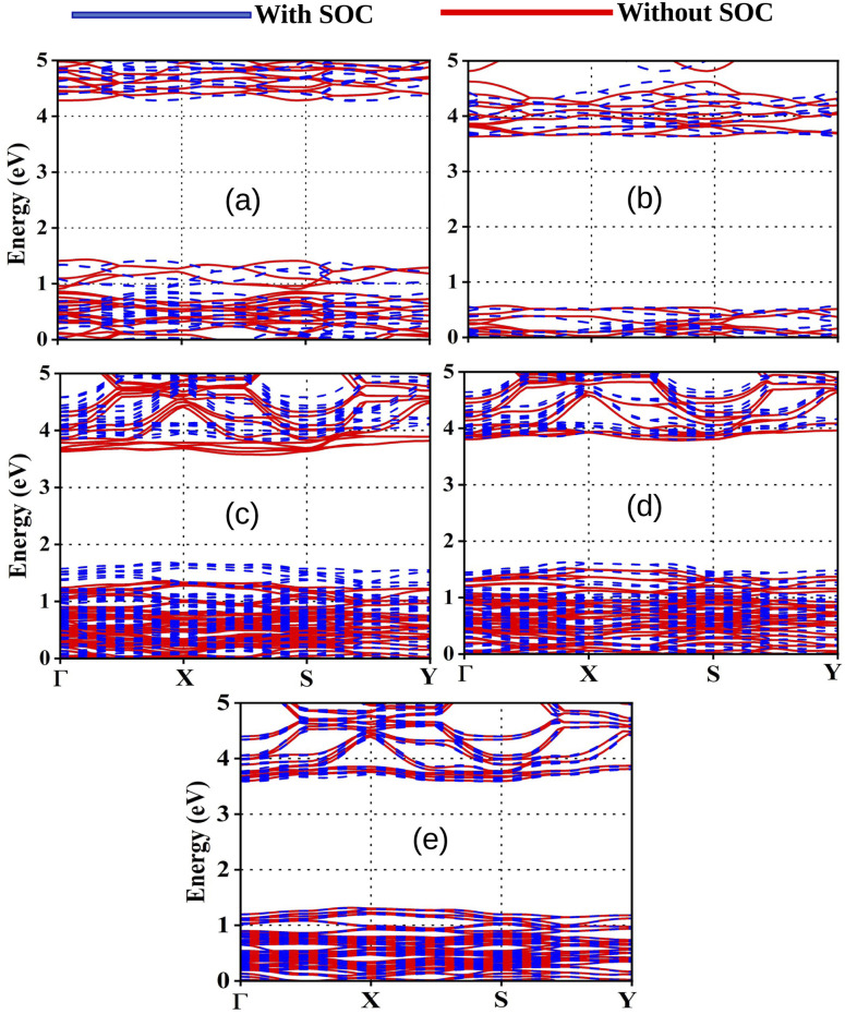
To investigate the electronic properties of our studied compounds we have calculated fundamental band gap values and the same are reported in Table 3. The corresponding band structures are presented in Fig. 2. It has noteworthy that the band gap values should lie in the range 1 to 4 eV for OIHPs to act as semiconducting material for optoelectronics.47,48 From Table 3, it is observed that all the studied compounds exhibit the band gap values in the desirable range. This indicates that our designed compounds have potential to be used in photovoltaics. It has been observed from Fig. 2 that the minimum direct band gap is obtained between Γ and S symmetry points. Several sets of bands have been observed in the band structure. These bands mainly corresponds to the 5p states of I below the Fermi level and 4s and 5s states of Ge and Sn above the Fermi level. However, 2p and 1s states of C, N and H have very little contribution towards the band structure. Moreover, the observed broad valence band maximum (VBM) and conduction band minimum (CBM) indicates the non local nature of these states.49 On the other hand, the observed strong fluctuations in the bottom conduction bands indicate faster transportation of photo-electrons.49 However, we have observed some flat bands in the bottom of the valence band due to the attribution of destructive interferences of wave functions in the lattice. It has been observed from Table 3 that the band gap values for compounds slightly increase with increase in the Ge content. From Table 3 it is observed that DMASn0.75Ge0.25I3 exhibits the lowest value of band gap among the studied compounds. However, mixed Sn–Ge based perovskite materials exhibit lower band gap values than their single metal atom counterparts.
Calculated band gaps of our studied compounds.
| Compounds | CBM (eV) | VBM (eV) | Band gap (eV) | |
|---|---|---|---|---|
| DMASnI3 | Non SOC | 4.28 | 1.43 | 2.84 |
| SOC | 4.19 | 1.42 | 2.77 | |
| DMAGeI3 | Non SOC | 3.63 | 0.57 | 3.05 |
| SOC | 3.59 | 0.51 | 3.08 | |
| DMASn0.75Ge0.25I3 | Non SOC | 3.58 | 1.35 | 2.23 |
| SOC | 3.85 | 1.66 | 2.19 | |
| DMASn0.50Ge0.50I3 | Non SOC | 3.78 | 1.51 | 2.27 |
| SOC | 3.84 | 1.61 | 2.23 | |
| DMASn0.25Ge0.75I3 | Non SOC | 3.59 | 1.29 | 2.30 |
| SOC | 3.59 | 1.29 | 2.30 |
Fig. 2. Calculated band structures of (a) DMASnI3, (b) DMAGeI3, (c) DMASn0.75Ge0.25I3, (d) DMASn0.50Ge0.50I3 and (e) DMASn0.25Ge0.75I3.
To have correct description of band gaps we have also performed spin orbit coupling (SOC) calculations with fully relativistic pseudopotentials. The obtained band gap values of our studied compounds incorporating SOC effect are also reported in Table 3. The inclusion of SOC slightly reduces the band gap values of all the compounds due to the change in the value of CBM and VBM. It has been also observed from Fig. 2 that SOC effect is very less pronounced for calculated band gaps of the compounds with higher amount of Sn content. However, the SOC effect is even negligible for calculated band gap of the compounds with higher amount of Ge. This may be due to the lighter weight of Ge in comparison to Sn.50
3.3.2. Density of states
In order to explore the reason for observed modulation of band gaps of our studied perovskite materials we have carried out total density of states (TDOS) and partial density of states (PDOS) calculation and the respective plots are provided in Fig. 3. The TDOS plots reveal that valence band of all the studied compounds exhibit the higher density of states which in turn indicates the semiconducting nature of our studied material.20 Besides it has also been observed from DOS calculation that the Fermi level is situated in between the CBM and VBM. The Fermi level is affected by the electron densities of the p-states of the Sn, Ge and I atoms respectively.51 PDOS spectra manifests that the electronic states of Sn, Ge and I are responsible for the alteration of the band gaps. The 5p states of I atoms have greater contribution towards VBM with little contribution from the 4s and 5s states of Ge and Sn. However, the 4p and 5p states of Ge and Sn has higher contribution towards the conduction band along with little contribution from 5p states of I atoms. It has also been observed from DOS spectra that with increase in the amount of Ge content the contribution of Ge (4p) states increases at conduction band. However, the negligible contribution of 2p states of C, N and 1s state of H to the DOS spectrum indicates that there is no covalent interaction between the organic cation (DMA) and the inorganic M–X (M = Sn and Ge, X = I) framework. Further it has been observed from Table 3 that the compounds dopped with Ge/Sn exhibits lower band gap values than DMASnI3/DMAGeI3 due to the change in composition of CBM which results in the lowering of band gaps. We have schematically illustrated the formation of CBM and VBM in Fig. 4.
Fig. 3. Plot of PDOS of (a) DMASnI3, (b) DMAGeI3, (c) DMASn0.75Ge0.25I3, (d) DMASn0.50Ge0.50I3 (e) DMASn0.25Ge0.75I3 and (f) TDOS of the studied compounds.
Fig. 4. Simplified energy level diagram of VBM and CBM (a) energy diagram of DMASnI3 and DMAGeI3, (b) energy level diagram of mixed DMA(Sn–Ge)I3.
3.3.3. Bader charge analysis
The Bader charge analysis have been performed based on the pseudo valence density by employing the PBE exchange correlation functional for all the studied compounds to predict the electronic and structural properties and the respective values are reported in Table 4. We have obeyed the charge neutrality of the unit cell during calculation of Bader charges. To have better effect of electric charge on the electronic properties of our studied perovskites we have divided the iodide ion into two categories viz. apical (Ia) and equatorial (Ie). It has been already reported that the formation energy decreases with increase in electric charge, which in turn indicates the thermodynamic stability of the perovskites due to ionic bonding.39,52 From Table 4 it is observed that the electric charges on organic cation is almost similar for all the studied compounds. It has also been observed from Table 4 that Sn2+/Ge2+ exhibits the maximum electric charge in DMASn0.75Ge0.25I3 in comparison to the rest of the compounds. However, the observed lower ΔE value in DMASn0.75Ge0.25I3 indicates its thermodynamic stability among all the studied compounds. Furthermore, it is also evident from Table 4 that both the compounds DMASn0.50Ge0.50I3 and DMASn0.25Ge0.75I3 exhibit suitable charge distribution. Besides, these two compounds also possess negative ΔE value. Therefore, these two compounds are also thermodynamically stable. The Bader charge analysis also provides a clear insight into the ionic interactions between the inorganic Sn/Ge–I framework and organic DMA+ cation.51 It has been observed from our calculation that the average charge per Sn/GeI3 and DMA+ units in all the studied compounds are −0.71 and +0.71. On the other hand, electric charges on Sn, Ge and I atoms in all compounds resemble to remarkable variation from pure ionic interactions. This indicates the existence of combined covalent and ionic bonding properties between Sn/Ge and I atoms. Moreover, the hybridization of 5s, 5p, 4s and 4p states of Sn and Ge with the 5p states of I at the top of the valence bands also support the covalent bonding characteristics of Sn/Ge–I framework as shown in Fig. 3. In DMA+ cation the positive charge contribution is mostly from the –CH3 groups. Table 4 also manifests that there exist an ionic interaction between the –CH3 group and I atoms. From this calculation it can be inferred that compounds dopped with higher amount of Sn content possesses higher stability and may exhibit higher charge transfer rate among all the studied compounds. Besides, compounds dopped with mixed metal ion exhibits the higher value of electric charge and greater thermodynamic stability compared to the compounds with single metal cation counterparts.
Bader charge analysis for the studied compounds.
| Compounds | DMA | Sn/Ge | I a | I e | Sn/GeI3 |
|---|---|---|---|---|---|
| DMASnI3 | 0.71 | 1.05 | −0.56 | −0.55 | −0.63 |
| DMAGeI3 | 0.67 | 0.80 | −0.52 | −0.52 | −0.76 |
| DMASn0.75Ge0.25I3 | 0.72 | 1.07/0.94 | −0.57 | −0.57 | −0.67 |
| DMASn0.50Ge0.50I3 | 0.72 | 0.95/0.96 | −0.56 | −0.55 | −0.73 |
| DMASn0.25Ge0.75I3 | 0.74 | 0.94/0.94 | −0.58 | −0.57 | −0.78 |
3.4. Optical properties
To investigate the optical properties of our studied compounds we have calculated the real and imaginary part of dielectric function (ε) for all the studied compounds by employing epsilon.x post processing code embodied in Quantum Espresso program. Dielectric function is crucial for exploring optical and electronic properties of perovskite materials. The coulomb interaction taking place between electrons and holes can be demonstrated by taking into account ε. It has been reported that an increase in ε decreases the coulomb interaction between electrons and holes, thereby accelerates the charge separation by reducing the exciton binding energy (Eb).53,54 It has also been reported that the higher value of ε indicates that the material can hold large quantities of charge for longer period of time which in turn enhances the photovoltaic performance of semiconducting materials.55,56 The real part of dielectric function (ε1) is a measure of the polarization of the material and the imaginary dielectric function (ε2) is a measure of the rate of losses of the radiation energy.57 Besides, the real part of dielectric function also expresses the change in wavelength of electromagnetic spectrum compared to vacuum and the imaginary part describes the absorption.57 When a beam of light (electromagnetic radiation) incident on a material, the optical response of the material can be expressed in terms of complex dielectric function, ε(ω) = ε1(ω) + iε2(ω).58 The imaginary part of the dielectric function is calculated from the momentum matrix elements between the occupied and unoccupied wave functions. However, with the help of Kramer's–Kronig relation (eqn (8)) we can compute the dispersion of the real part of dielectric function by taking into consideration the imaginary part.59
 |
8 |
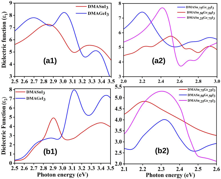
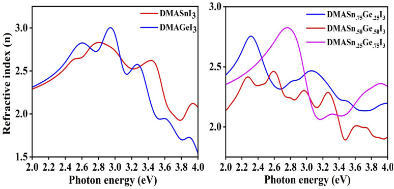
where P represents the Cauchy principal value. The calculated ε1 and ε2 for all the studied compounds are presented in Fig. 5. It is clearly visible from the plots of dielectric function that all the compounds exhibit higher value of ε in the visible range of electromagnetic spectrum (0–3 eV). Moreover, from Fig. 5 it is also observed that DMASn0.25Ge0.75I3 exhibits the highest value of dielectric function at energy 2.4 eV. However, DMASnI3 exhibits the highest value of dielectric function in the energy range of 3–3.2 eV. We have also calculated the refractive index (n) for all the studied compounds from the values of ε1 and ε2 and the respective plots are presented in Fig. 6. Refractive index is defined as a physicochemical property as its value changes upon irradiation of light due to the interaction between atoms in a material.58 It has been reported that the dielectric function and complex refractive index are alike to each other. The refractive index is usually used to measure the response of a material upon transmission of light through it.60 From Fig. 6 it has been observed that refractive index of all the compounds follow the similar pattern with ε1. It can be inferred from this observation that the compounds having mixed metal content exhibits the dielectric function in the visible range of electromagnetic spectrum.
Fig. 5. Plot of real (ε1) (a) and imaginary (ε2) (b) part of dielectric function of studied compounds.
Fig. 6. Plot of refractive index (n) of studied compounds.
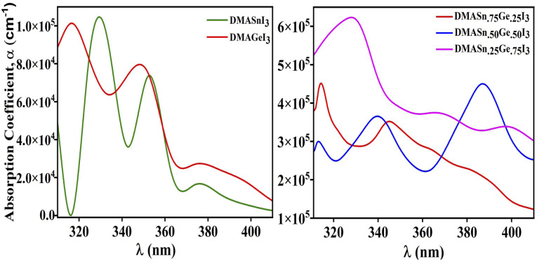
Furthermore, to envisage the optical absorption ability of our studied perovskite materials in detail we have simulated the absorption coefficient by employing time-dependent density functional theory formalism embodied in Quantum Espresso program package. The absorption coefficient has been calculated from the real and imaginary part of complex dielectric function.61 It is noteworthy that intense optical absorption in the visible range of electromagnetic spectrum is necessarily important for photovoltaic materials. The plot of UV-Vis spectra of the studied compounds have been presented in Fig. 7. From Fig. 7 it has been observed that all the compounds under investigation exhibit strong absorption in the nearly visible and visible range of electromagnetic spectrum. We have noticed three major absorption coefficient with minor shoulder peak in the absorption spectra at wavelengths 330 nm, 350 nm and 390 nm for the compounds DMASn0.25Ge0.75I3, DMASn0.75Ge0.25I3 and DMASn0.50Ge0.50I3 respectively. It has also been observed from Fig. 7 that DMASn0.50Ge0.50I3 shows higher values of absorption coefficient in the visible range of electromagnetic spectrum. Whereas, DMASnI3 and DMAGeI3 exhibit absorption coefficient at around 330 and 320 nm in the electromagnetic spectrum. From the values of α and ε it can be inferred that compounds with mixed metal cations are better candidates for photovoltaic applications compared to single metal hybrid halide perovskites.
Fig. 7. Plot of UV-visible spectra of studied compounds.
3.5. Photovoltaic performance
To investigate the photovoltaic performance of our studied compounds we have calculated the values of Voc, Jsc and theoretical PCE (η) by using eqn (4) to (7). The obtained results are presented in Table 5. It has been observed that the Jsc value increases with decrease in band gap.33,41 Furthermore, Table 5 manifests that with increase in Ge content the band gap values moderately get increased which results in the lowering of Jsc and PCE. Therefore, DMASn0.75Ge0.25I3 exhibits the highest value of PCE (17.42%) among the studied compounds. Besides, from Table 5 it has been also observed that the low Eloss value (0.5 eV) elevates the Voc and as a result improves the PCE of the studied perovskite materials.
Calculated Voc, Jsc and η values of the studied compounds.
| Compounds | E loss (eV) | V oc (eV) | J sc (mA cm−2) | η% |
|---|---|---|---|---|
| DMASnI3 | 0.7 | 2.14 | 2.80 | 6.00 |
| 0.5 | 2.34 | 6.55 | ||
| DMASnI3 | 0.7 | 2.36 | 1.56 | 3.68 |
| 0.5 | 2.56 | 4.00 | ||
| DMASn0.75Ge0.25I3 | 0.7 | 1.53 | 10.07 | 15.40 |
| 0.5 | 1.73 | 17.42 | ||
| DMASn0.50Ge0.50I3 | 0.7 | 1.57 | 9.45 | 14.84 |
| 0.5 | 1.77 | 16.73 | ||
| DMASn0.25Ge0.75I3 | 0.7 | 1.58 | 9.25 | 14.62 |
| 0.5 | 1.78 | 16.47 |
4. Conclusions
Here, we have tried to tune the optoelectronic properties of pure Sn and Ge based perovskites by mixing Sn and Ge with varying composition along with incorporating DMA as organic cation and placing iodide ion as halide at apical and equatorial positions. It has been confirmed from the formation energy, TF and μ values that all the compounds are thermodynamically stable and forms three dimensional perovskite structures. However, with increase in Ge content the band gap increases. Moreover, the band gap of single metal hybrid perovskite materials have higher value than the compounds having mixed metal in different compositions. As a result compounds having high amount of Sn content in mixed Sn and Ge based perovskites can act as a potential candidate for application in photovoltaics.
From the real and imaginary part of dielectric function it is also observed that all the compounds containing mixed Sn–Ge possess higher value of dielectric function in visible range of electromagnetic spectrum. Among the studied compounds DMASn0.50Ge0.50I3 exhibits the highest value of both real and imaginary dielectric function. From optical absorption calculation it is observed that all the Sn–Ge based compounds possess absorption maximum in the near visible and visible range of electromagnetic spectrum. Moreover, the maximum PCE (17.42%) has been observed for DMASn0.75Ge0.25I3 which in turn implies its potential to be used in photovoltaic applications.
In short our investigation reveals that mixed Sn–Ge based hybrid perovskite materials can be chosen as a suitable candidate in lieu of the toxic Pb content in perovskite solar cells. We strongly feel that our work will open up a new horizon for researchers for fabrication of Pb-free hybrid halide perovskite materials, which will be beneficial to the world.
Conflicts of interest
There are no conflicts to declare.
Supplementary Material
Acknowledgments
The authors would like to acknowledge the Department of Science and Technology (SB/FT/CS-077/2013), India for the financial support. The authors would like to acknowledge the University Grants Commission for UGC-BSR Research start-up-grant (NO.F.30.-122/2015(BSR)), Gauhati University for providing the research facilities and financial support.
Electronic supplementary information (ESI) available: Optimized coordinates of the studied compounds and energies of VBM, CBM and band gap values of the reference compound. See https://doi.org/10.1039/d2ra05256c
References
- Noel K. N. Stranks D. S. Abate A. Wehrenfennig C. Guarnera S. Haghighirad A.-A. Sadhanala A. Eperon E. G. Pathak K. S. Johnston B. M. Petrozza A. Herza M. L. Snaith J. H. Energy Environ. Sci. 2014;7:3061–3068. [Google Scholar]
- Green M. A. Ho-Baillie A. Snaith J. H. Nature. 2014;8:506–514. [Google Scholar]
- Kojima A. Teshima K. Shirai Y. Miyasaka T. J. Am. Chem. Soc. 2009;131:6050–6051. doi: 10.1021/ja809598r. [DOI] [PubMed] [Google Scholar]
- Wu T. Qin Z. Wang Y. Wu Y. Chen W. Zhang S. Cai M. Dai S. Zhang J. Liu J. Nano-Micro Lett. 2021;13:1–18. doi: 10.1007/s40820-021-00672-w. [DOI] [PMC free article] [PubMed] [Google Scholar]
- Deng Y. Brackle C. H. V. Dai X. Zhao J. Chen B. Huang J. Sci. Adv. 2019;5:eaax7537. doi: 10.1126/sciadv.aax7537. [DOI] [PMC free article] [PubMed] [Google Scholar]
- Wang R. Huang T. Xue J. Tong J. Zhu K. Yang Y. Nat. Photonics. 2021;15:411–425. [Google Scholar]
- Li X. Zhang F. Wang J. Tong J. Xu T. Zhu K. Nature Sustainability. 2021;4:1038–1041. [Google Scholar]
- Sa R. Liu D. Chen Y. Ying S. ACS Omega. 2020;5:4347–4351. doi: 10.1021/acsomega.9b04484. [DOI] [PMC free article] [PubMed] [Google Scholar]
- Quarti C. Mosconi E. Angelis D. F. Phys. Chem. Chem. Phys. 2015;17:9394–9409. doi: 10.1039/c5cp00599j. [DOI] [PubMed] [Google Scholar]
- Umebayashi T. Asai K. Kondo T. Nakao A. Phys. Rev. B: Condens. Matter Mater. Phys. 2003;17:155405. [Google Scholar]
- Mosconi E. Amat A. Nazeeruddin K. M. Gratzel M. Angelis D. F. J. Phys. Chem. C. 2013;117:13902–13913. [Google Scholar]
- Alwarappan G. Alam R. M. Hassan I. M. W. Shibl F. M. Alfalah S. Patil S. Nekovei R. Verma A. Sol. Energy. 2019;189:86–93. [Google Scholar]
- Dang Y. Liu Y. Sun Y. Yuan D. Liu X. Lu W. Liu G. Xia H. Tao X. CrystEngComm. 2015;17:665–670. [Google Scholar]
- Baikie T. Fang Y. Kadro J. M. Schreyer M. Wei F. Mhaisalkar S. G. Graetzel M. White T. J. J. Mater. Chem. A. 2014;1:5628–5641. [Google Scholar]
- Nishat M. Hossain M. K. Hossain M. R. Khanom S. Ahmed F. Hossain M. A. RSC Adv. 2022;12:13281–13294. doi: 10.1039/d1ra08561a. [DOI] [PMC free article] [PubMed] [Google Scholar]
- Chen R. Hou D. Lu C. Zhang J. Liu P. Tian H. Zeng Z. Xiong Q. Hu Z. Zhu Y. Sustainable Energy Fuels. 2018;2:1093–1100. [Google Scholar]
- Chutia T. Kalita D. J. Mol. Phys. 2022;120:e2037772. [Google Scholar]
- Stoumpos C. C. Malliakas C. D. Kanatzidis M. G. Inorg. Chem. 2013;52:9019–9038. doi: 10.1021/ic401215x. [DOI] [PubMed] [Google Scholar]
- Grazulis S. Chateigner D. Downs R. T. Yokochi A. F. T. Quiros M. Lutterotti L. Manakova E. Butkus J. Moeck P. Bail A. L. J. Appl. Crystallogr. 2009;42:726–729. doi: 10.1107/S0021889809016690. [DOI] [PMC free article] [PubMed] [Google Scholar]
- Paschal C. Pogrebnoi A. Pogrebnaya T. Seriani N. SN Appl. Sci. 2020;2:718. [Google Scholar]
- Giannozzi P. Baroni S. Bonini N. Calandra M. Car R. Cavazzoni C. Ceresoli D. Chiarotti G. Cococcioni L. M. Dabo I. Corso A. D. Gironcoli S. d. Fabris S. Fratesi G. Gebauer R. Gerstmann U. Gougoussis C. Kokalj A. Lazzeri M. Martin-Samos L. Marzari N. Mauri F. Mazzarello R. Paolini S. Pasquarello A. Paulatto L. Sbraccia C. Scandolo S. Sclauzero G. Seitsonen A. P. Smogunov A. Umari P. Wentzcovitch R. M. J. Phys.: Condens. Matter. 2009;21:395502. doi: 10.1088/0953-8984/21/39/395502. [DOI] [PubMed] [Google Scholar]
- Perdew J. P. Ruzsinszky A. Csonka G. I. Vydrov O. A. Scuseria G. E. Constantin L. A. Zhou X. Burke K. Phys. Rev. Lett. 2008;100:136406. doi: 10.1103/PhysRevLett.100.136406. [DOI] [PubMed] [Google Scholar]
- Liu J. Xue Y. Wang Z. Xu Z.-Q. Zheng C. Weber B. Song J. Wang Y. Lu Y. Zhang Y. Bao Q. ACS Nano. 2016;10:3536–3542. doi: 10.1021/acsnano.5b07791. [DOI] [PubMed] [Google Scholar]
- Perdew J. P. Burke K. Ernzerhof M. Phys. Rev. Lett. 1996;77:3865–3868. doi: 10.1103/PhysRevLett.77.3865. [DOI] [PubMed] [Google Scholar]
- Wang Y. Liu Y. Wu Y. Jiang J. Liu C. Liu W. Gao K. Cai H. Wu X. CrystEngComm. 2020;22:7090–7094. [Google Scholar]
- Dang Y. Zhong C. Zhang G. Ju D. Wang L. Xia S. Xia H. Tao X. Chem. Mater. 2016;28:6968–6974. [Google Scholar]
- Vanderbilt D. Phys. Rev. B: Condens. Matter Mater. Phys. 1990;41:7892–7895. doi: 10.1103/physrevb.41.7892. [DOI] [PubMed] [Google Scholar]
- Quarti C. Marchal g. N. Beljonne D. J. Phys. Chem. Lett. 2018;9:3416–3424. doi: 10.1021/acs.jpclett.8b01309. [DOI] [PubMed] [Google Scholar]
- Toby B. H. J. Appl. Crystallogr. 2001;34:210–213. [Google Scholar]
- Even J. Pedesseau L. Jancu J. M. Katan C. J. Phys. Chem. Lett. 2013;4:2999–3005. [Google Scholar]
- Monkhorst H. J. Pack J. D. Phys. Rev. B: Solid State. 1976;13:5188–5192. [Google Scholar]
- Zeba I. Ramzan M. Ahmad R. Shakil M. Rizwan M. Rafique M. Sarfraz M. Ajmal M. Gillani S. Solid State Commun. 2020;313:113907. [Google Scholar]
- Liu D. Li Q. Hu J. Sa R. Wu K. J. Phys. Chem. C. 2019;20:12638–12646. [Google Scholar]
- Mayengbam R. Tripathy K. S. Palai G. J. Phys. Chem. C. 2018;122:28245–28255. [Google Scholar]
- Hartono N. T. P. Sun S. Gélvez-Rueda M. C. Pierone P. J. Erodici M. P. Yoo J. Wei F. Bawendi M. Grozema F. C. Sher M.-j. J. Mater. Chem. A. 2019;7:23949–23957. [Google Scholar]
- Zhao Y. Zhu K. Chem. Soc. Rev. 2016;45:655–689. doi: 10.1039/c4cs00458b. [DOI] [PubMed] [Google Scholar]
- Becker M. Kluner T. Wark M. Dalton Trans. 2017;46:3500–3509. doi: 10.1039/c6dt04796c. [DOI] [PubMed] [Google Scholar]
- Yi Z. Ladi N. H. Shai X. Li H. Shena Y. Wang M. Nanoscale Adv. 2019;1:1276–1289. doi: 10.1039/c8na00416a. [DOI] [PMC free article] [PubMed] [Google Scholar]
- Yamamoto K. Iikubo S. Yamasaki J. Ogomi Y. Hayase S. J. Phys. Chem. C. 2017;121:27797–27804. [Google Scholar]
- Mayengbam R. Tripathy S. K. Palai G. J. Phys. Chem. C. 2018;122:28245–28255. [Google Scholar]
- Filip M. R. Verdi C. Giustino F. J. Phys. Chem. 2015;119:25209–25219. [Google Scholar]
- Snaith H. J. Adv. Funct. Mater. 2010;20:13–19. doi: 10.1002/adfm.201000367. [DOI] [PMC free article] [PubMed] [Google Scholar]
- Zhang T. Cai Z. Chen S. ACS Appl. Mater. Interfaces. 2020;12:20680–20690. doi: 10.1021/acsami.0c03622. [DOI] [PubMed] [Google Scholar]
- Chen Q. Marco N. D. Yang Y. M. Song T.-B. Chen C.-C. Zhao H. Hong Z. Zhou H. Yang Y. Nano Today. 2015;10:355–396. [Google Scholar]
- Koskin P. I. Mostovich A. E. Benassi E. Kazantsev S. M. J. Phys. Chem. C. 2017;121:23359–23369. [Google Scholar]
- Eperon G. E. Stranks S. D. Menelaou C. Johnston M. B. Herz L. M. Snaith H. J. Energy Environ. Sci. 2014;7:982–988. [Google Scholar]
- Xiao Z. Zhou Y. Hosono H. Kamiya T. Padture N. P. Chem.–Eur. J. 2018;24:2305–2316. doi: 10.1002/chem.201705031. [DOI] [PubMed] [Google Scholar]
- Mancini A. Quadrelli P. Amoroso G. Milanese C. Boiocchi M. Sironi A. Patrini M. Guizzetti G. Malavasi L. J. Solid State Chem. 2016;240:55–60. [Google Scholar]
- Wang Y. Gould T. Dobson J. F. Zhang H. Yang H. Yao X. Zhao H. Phys. Chem. Chem. Phys. 2014;16:1424–1429. doi: 10.1039/c3cp54479f. [DOI] [PubMed] [Google Scholar]
- Ma X.-X. Li Z.-S. Phys. Status Solidi B. 2019;256:1800427. [Google Scholar]
- Wang Y. Gould T. Dobson J. F. Zhang H. Yang H. Yao X. Zhao H. Phys. Chem. Chem. Phys. 2014;16:1424–1429. doi: 10.1039/c3cp54479f. [DOI] [PubMed] [Google Scholar]
- Liu D. Li Q. Hu J. Sa R. Wu K. J. Phys. Chem. C. 2019;123:12638–12646. [Google Scholar]
- Dong Y. Zhu R. Jia Y. J. Phys. Chem. C. 2021;125:14883–14890. [Google Scholar]
- Lin Q. Armin A. Nagiri R. C. R. Burn P. L. Meredith P. Nat. Photonics. 2015;9:106–112. [Google Scholar]
- Roknuzzaman M. Zhang C. Ostrikov K. K. Du A. Wang H. Wang L. Tesfamichael T. Sci. Rep. 2019;9:718. doi: 10.1038/s41598-018-37132-2. [DOI] [PMC free article] [PubMed] [Google Scholar]
- Hossain K. Khanom S. Israt F. Hossain M. Hossain M. Ahmed F. Solid State Commun. 2020;320:114024. [Google Scholar]
- Petzelt J. and Rychetský I., Encyclopedia of Condensed Matter Physics, Elsevier, Oxford, 2005, pp. 426–429 [Google Scholar]
- Mayengbam R. Srivastava A. Tripathy S. Palai G. J. Phys. Chem. C. 2019;123:23323–23333. [Google Scholar]
- Ghazanfar M. Azam S. Nasir M. F. Khan R. J. Solid State Chem. 2021;301:122335. [Google Scholar]
- Liu B. Soe C. M. M. Stoumpos C. C. Nie W. Tsai H. Lim K. Mohite A. D. Kanatzidis M. G. Marks T. J. Singer K. D. Sol. RRL. 2017;1:1700062. [Google Scholar]
- Liu D. Li Q. Hu J. Jing H. Wu K. J. Mater. Chem. 2019;7:371–379. [Google Scholar]
Associated Data
This section collects any data citations, data availability statements, or supplementary materials included in this article.


