Abstract
650 V SiC planar MOSFETs with various JFET widths, JFET doping concentrations, and gate oxide thicknesses were fabricated by a commercial SiC foundry on two six-inch SiC epitaxial wafers. An orthogonal layout was used for the 650 V SiC MOSFETs to reduce the ON-resistance. The devices were packaged into open-cavity TO-247 packages for evaluation. Trade-off analysis of the static and dynamic performance of the 650 V SiC power MOSFETs was conducted. The measurement results show that a short JFET region with an enhanced JFET doping concentration reduces specific ON-resistance () and lowers the gate-drain capacitance (). It was experimentally shown that a thinner gate oxide further reduces , although with a penalty in terms of increased . A design with 0.5 m half JFET width, enhanced JFET doping concentration of cm−3, and thin gate oxide produces an excellent high-frequency figure of merit (HF-FOM) among recently published studies on 650 V SiC devices.
Keywords: SiC power MOSFET, JFET width, JFET doping concentration, gate oxide thickness, orthogonal P+ layout, gate-drain capacitance, high-frequency figure-of-merit (HF-FOM)
1. Introduction
Silicon carbide (SiC) power Metal-Oxide-Semiconductor Field-Effect Transistors (MOSFETs) have been commercialized in a wide range of voltage ratings from 600 to 1700 . The launch of 650 SiC MOSFETs addresses the lower voltage applications, which have traditionally been dominated by Si devices. SiC power MOSFETs outperform Si devices in low switching loss, high switching frequency, low ON-resistance (), and high temperature operations [1,2,3]. Hence, designing SiC power MOSFETs with lower and superior switching performance needs to be studied in detail.
JFET region design, including the JFET width and doping concentration, plays a crucial role in optimizing the and switching performance of SiC MOSFETs [4]. Studies of JFET region design for 1 and SiC MOSFETs [5,6] have demonstrated that optimizing JFET width and enhancing the doping concentration of the JFET region can reduce the JFET region resistance and lead to smaller of SiC power MOSFETs. In addition, JFET region design affects the gate-drain capacitance (); determines the switching performance of 650 SiC MOSFETs, primarily due to the well-known Miller effect [7]. The product of and is referred to as the high-frequency figure of merit (HF-FOM) [8]. A lower HF-FOM implies better high-frequency switching performance for devices. Sung and Baliga have reported that a narrow JFET width with a high JFET doping concentration decreases and improves HF-FOM [9]. The gate-source and the drain-source capacitances, and , respectively, are affected by JFET width variation through the pitch of the cell, while and contribute to the switching loss of SiC power MOSFETs [10].
Gate oxide thickness plays a role in the static and dynamic performance of SiC MOSFETs. As an example, a 27 nm gate oxide was used for 650 SiC power MOSFETs by Agarwal et al. [11,12], resulting a 1.7× better specific ON-resistance () compared to MOSFETs with a 55 nm gate oxide. Under a certain operation gate voltage, a thinner gate oxide decreases by reducing the channel resistance. However, a thin gate oxide increases the gate oxide capacitance (), and hence increases and . In addition, a thin gate oxide raises gate oxide reliability issues when sustaining high gate oxide fields [13].
In this work, the authors analyze the performance trade-offs, including threshold voltage (), , breakdown voltage (), and parasitic capacitances for 650 SiC MOSFETs with different JFET widths, JFET doping concentrations, and gate oxide thicknesses. The 650 SiC power MOSFETs were fabricated on two six-inch SiC epitaxial wafers by a commercial foundry. The design details and fabrication information are presented in Section 2. The preliminary wafer-level characterizations have been published in [14]. The fabricated devices were packaged for static and dynamic measurements. The experimental methods are explained in Section 3. In Section 4, the experimental results are presented and discussed. Section 5 provides further analysis of the performance trade-offs for the 650 SiC MOSFETs.
2. Device Design and Fabrication
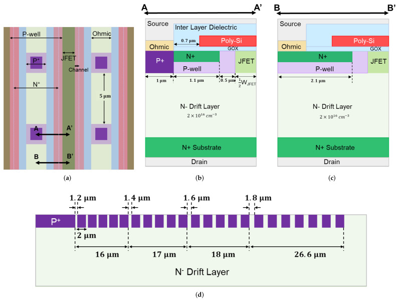
The layout design of a 650 SiC MOSFET is shown in Figure 1a. The layout is in a stripe pattern, with square regions located periodically in the center of the P-well stripe. The orthogonal layout reduces the of the MOSFETs by reducing the cell pitch compared to the traditional linear striped layout. The cross-section along the A-A cutline is shown in Figure 1b. The half-cell pitch consists of width (1 m), source width (1.1 m), channel length (0.5 m), and half JFET width (). The spacing between the source contact and polysilicon gate is 0.7 m. The ohmic contact width is 1 m. The cross-section along B-B′ (Figure 1c) shows the layout with only source. The extended source replaces the in the A-A half-cell pitch and produces a total source width of 2.1 m. Four devices with different half-JFET widths were designed ( = 0.4, 0.5, 0.6, and 0.75 m).
Figure 1.
(a) Layout design of a SiC power MOSFET with located periodically in the center of P-well stripe; (b) A-A′ cross-sectional view showing both and ; (c) B-B′ cross-sectional view showing extended source; (d) cross-sectional view of the edge termination of the fabricated 650 SiC power MOSFETs.
Twenty-two guard rings were used as the edge termination for all layouts. Each guard ring had a width of 2 m. A cross-sectional view of the edge termination is shown in Figure 1d. The edge termination can be divided into four sections. The spacing for each section is illustrated in Figure 1d; spacing was identical in each section. The total length of the edge termination was 77.6 m.
Different JFET doping concentrations () and gate oxide thicknesses () were utilized during the fabrication of the devices. The devices were fabricated on two six-inch 4H-SiC wafers (wafer 1 and wafer 2) with n-type epitaxial layers on substrates. The substrates were thinned to reduce the resistance. The epitaxial layer was doped with nitrogen with a doping concentration of cm−3. Ion implantation of nitrogen was used to form the JFET region and source; = cm−3 and = cm−3 were used for wafers 1 and 2, respectively. Aluminum ions were implanted to form the P-well and region. The gate oxide was grown after the implantation and activation annealing processes. The gate oxide thicknesses on wafers 1 and 2 are represented as (36∼44 nm) and (32∼38 nm), respectively; is 12.5% less than . Details of the gate oxide thicknesses have been discussed previously in [14]. Self-alignment technology was utilized to form the MOS channel. Fabrication was completed following the standard process flow of commercial SiC MOSFETs.
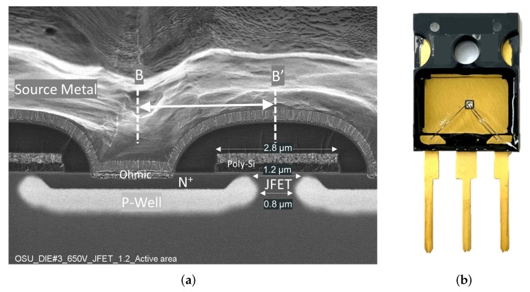
The design parameters and experimental results for all devices are summarized in Table 1 (Section 5). Figure 2a shows a cross-sectional SEM image (along BB’ in Figure 1c) of the fabricated 650 SiC MOSFET ( = 0.6 m) on wafer 1. Due to the lateral straggle of Aluminum implantation in the P-well, the narrowest portion of the JFET region is reduced by 0.2 m on each side.
Figure 2.
(a) Cross-sectional SEM image along B-B′ of the fabricated 650 SiC power MOSFETs with = 0.6 m and (b) 650 SiC power MOSFET in a open-cavity TO-247 package.
3. Experimental Methods
3.1. Device Packaging
The fabricated MOSFETs were diced and packaged into open cavity TO-247 packages, as shown in Figure 2b. A single 5-mil aluminum wire bond was used for the gate terminal, while two-wire bonds were attached on the the source area to decrease the parasitic resistance. Silicone dielectric gel was used to fill the cavity to protect the bare die. Five copies of each layout design on wafers 1 and 2 were packaged.
3.2. Device Characterization
The static performance of the MOSFETs, including the transfer, output, and blocking characteristics, were measured with a Keysight B1506A semiconductor parameter analyzer. We extracted at a drain current of 1 from the transfer characteristics tested under a drain bias of 100 mV. The output characteristics were measured under a gate bias of 20 V, with the drain voltage swept from 0 to 2 V. We obtained the of the device under test (DUT) at a drain bias of 1.5 V; was obtained from the blocking I-V characteristics at a current of 100 A, while , , and were measured up to a drain bias of 400 at a frequency of 100 using a Keysight B1505A semiconductor parameter analyzer.
4. Device Characteristics and Discussion
The measured device characteristics for the packaged 650 SiC MOSFETs with different designs are illustrated and compared in this section.
4.1. Threshold Voltage
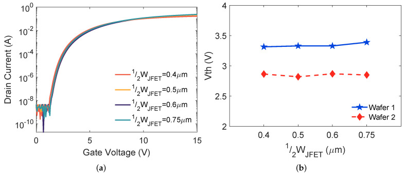
The transfer characteristics for the devices with different on wafer 1 are plotted in Figure 3a. Typical transfer curves of SiC MOSFETs were obtained from all the DUTs. The average from the five copies of each design is plotted in Figure 3b. Minimal variation was observed for wafers 1 and 2 when increasing .
Figure 3.
(a) Measured transfer characteristics of the packaged 650 SiC MOSFETs on wafer 1 and (b) variation as a function of for MOSFETs on wafers 1 and 2.
The of the MOSFETs on wafer 2 is smaller than wafer 1, as shown in Figure 3b. The thinner gate oxide contributes to the reduction; here, is defined as [8]:
| (1) |
where is the metal–semiconductor work function difference, is the permittivity of SiC, k and T are the Boltzmann constant and temperature, respectively, is the intrinsic carrier concentration of SiC, q is the electric charge, is the total effective charge in the oxide (the sum of the fixed and interface charges), and is the net p-type doping concentration at the channel region; is the gate oxide capacitance, which is given as
| (2) |
where is the permittivity of oxide. Comparing wafer 2 to wafer 1, higher reduces by the effect of the counter doping at the surface. Additionally, the thinner gate oxide of wafer 2 increases . According to (1), the reduced at the surface and increased lead to smaller of the MOSFETs on wafer 2.
4.2. Specific ON-Resistance
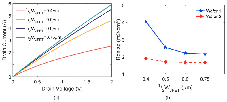
Figure 4a shows the output characteristics at a gate bias of 20 V for devices on wafer 1. Drain current increases with a wider JFET region. Figure 4b plots versus variation. For both wafers 1 and 2, is reduced when increasing because a larger provides lower JFET region resistance [14]. With the same , reduction from wafer 1 to wafer 2 is contributed by thinner gate oxide and higher . A considerable (1.6×) reduction is observed when rises from 0.4 m to 0.5 m on wafer 1, while the tendency is weaker for wafer 2. These results indicate that thinner gate oxide and higher make less susceptible to variation.
Figure 4.
(a) Measured output characteristics of the SiC MOSFETs on wafer 1 and (b) variation as a function of for MOSFETs on wafers 1 and 2.
4.3. Breakdown Voltage
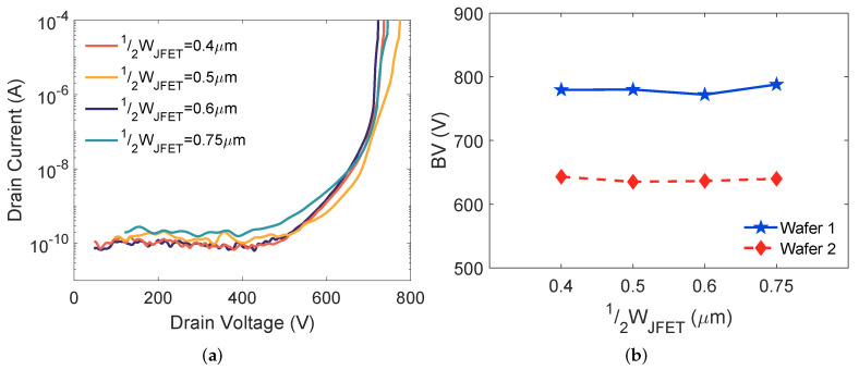
The blocking characteristics for MOSFETs on wafer 1 are shown in Figure 5a. All DUTs maintain low leakage currents (∼100 pA) under drain voltage up to 550 V. The drain to source breakdown of a planar SiC MOSFET is triggered by avalanche breakdown, and both and have little effect on the BV determined by avalanche breakdown [5]. Our experimental results (Figure 5b) show that the BV of 650 SiC MOSFETs is minimally changed by variation.
Figure 5.
(a) Measured blocking characteristics of the SiC MOSFETs on wafer 1 and (b) Maximum as a function of for MOSFETs on wafers 1 and 2.
A maximum BV of about 780 is achieved for devices on wafer 1. The BV for MOSFETs on wafer 2 is . The 18% BV drop from wafer 1 to wafer 2 is mainly caused by the difference in drift layer doping. The drift layer doping concentrations can be extracted from the C-V measurement of MOS capacitors on both wafers [15]. The extracted drift layer doping concentrations are cm−3 and cm−3 for wafers 1 and 2, respectively. This difference explains the reduction of BV on wafer 2.
Although BV does not change with variation, a smaller improves the gate oxide reliability of the MOSFETs by better shielding the gate oxide on the top of the JFET region from high oxide fields under the blocking condition [14,16]. These high oxide fields may cause high gate leakage currents, degrade the gate oxide, and reduce the oxide lifetime [13,17], and can lead to failures during High-Temperature Reverse Bias (HTRB) testing.
4.4. Device Capacitances
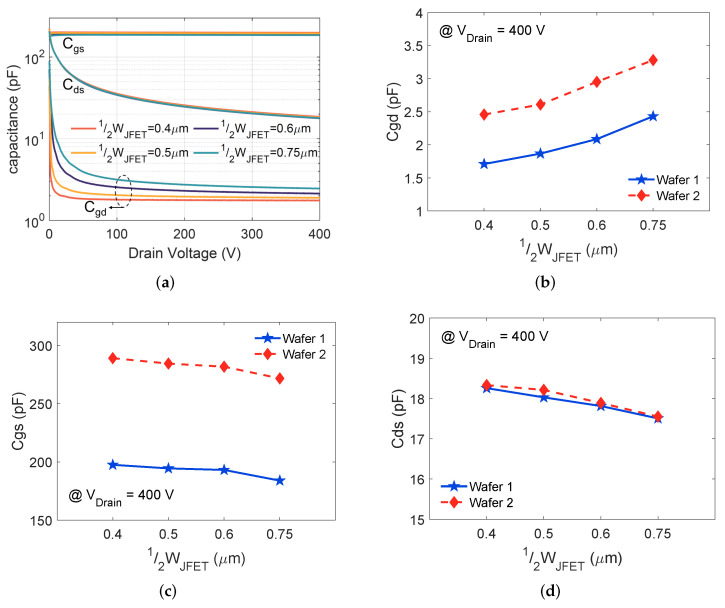
The device capacitances as a function of the applied drain bias for 650 V MOSFETs on wafer 1 are shown in Figure 6a. As expected, the measured and are nonlinear functions of the drain bias, while stays relatively constant with increasing drain bias. The extracted , , and as function of for the MOSFETs on wafers 1 and 2 are shown in Figure 6b–d, respectively.
Figure 6.
(a) Measured device capacitances vs. drain voltage at 100 of the SiC MOSFETs on wafer 1, (b) , (c) , and (d) variation as a function of for MOSFETs on wafers 1 and 2.
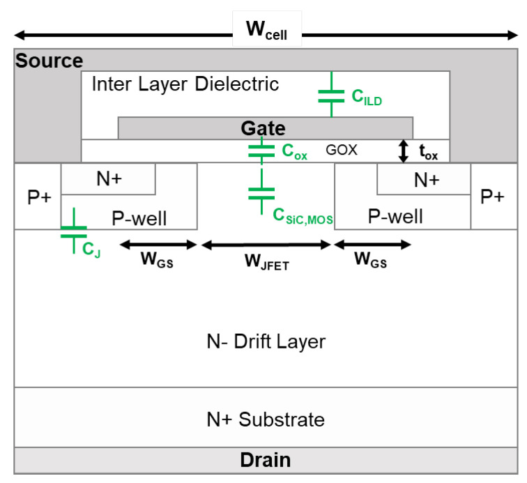
When extending , increases. For a planar SiC MOSFET, is formed by the overlap between the gate and drain electrodes. A complete cell cross-section in Figure 7, illustrating the various device capacitance components. Here, is composed of and depletion region capacitance () under the gate oxide; is defined as follows:
| (3) |
Figure 7.
Device capacitance components.
Equation (3) is based on [8], where refers to the cell pitch, represents the active area of the device, stays constant for the devices with the same , and is determined by the depletion layer thickness under the gate oxide, which does not change for devices with the same and which sustain a specific drain bias. According to (3), increases when increasing , which agrees with the measured results for both wafers 1 and 2 in Figure 6b.
Comparing wafer 2 to wafer 1, drops by 12.5%. Correspondingly, increases by 14.3% and leads to increasing. The enhanced of wafer 2 affects by changing the thickness and the width of the depletion layer [7,18]. It is challenging to identify the change of quantitatively, as the depletion layer varies with the gate-drain bias, p-well potential, and doping concentration of the JFET and drift layer [19]. The results in [9] demonstrate that a higher leads to a higher . Thus, the overall outcome from lowering and increasing is the increase of . The measured for MOSFETs on wafer 2 is about 1.4× higher than those of wafer 1 under a given , as shown in Figure 6b.
Note that consists of the overlap capacitance of the gate electrode with source plus channel region and the parallel capacitance across the gate and source metallization () [20]; in the active area of a 650 SiC MOSFET is addressed as
| (4) |
where is the total length of the overlap between gate and source and the channel region and is the inter-layer dielectric capacitance, which stays constant for all the devices due to the same fabrication process being used for wafers 1 and 2.
Among the designs on the same wafer, increasing reduces the coefficients of and in (4) and leads to the increase of . The measured verifies the variation for both wafer 1 and wafer 2 in Figure 6c. For a specific , a thinner gate oxide increases , and hence result in a higher according to (4). This explains the higher measured on wafer 2 compared to on wafer 1.
As is driven by the depletion layer formation at the P-well and drift region interface, the total in the active area of a 650 SiC MOSFET is expressed as
| (5) |
where is the junction capacitance per unit area, which is determined by the depletion layer thickness. All the DUTs in this work have similar doping concentration of the epi-layer. The bottom of the P-well is heavily doped, meaning that the depletion thickness in the p-well region can be neglected. Thus, under a particular drain bias, the depletion layer thickness stays almost the same for all DUTs, which results in similar . According to (5), increasing reduces , corresponding to the measured results in Figure 6d for both wafer 1 and wafer 2. In addition, the measured under a certain is almost the same for the MOSFETs on both wafers, which is due to the fact that and are not involved in (5).
5. Trade-Offs
Table 1 summarizes the design information and experimental results for the 650 V SiC MOSFETs. HF-FOM is included to evaluate the performance of the devices.
The variation of influences and the device capacitance. When reducing the from 0.75 m to 0.4 m, (1) increases by 1.9× for wafer 1 and 1.1× for wafer 2; (2) decreases by 1.4× for wafer 1 and 1.3× for wafer 2; and (3) less than 7% and 4% increase are identified for and , respectively.
Comparing the performance of the MOSFETs on wafer 2 to those on wafer 1, higher and thinner gate oxide have the following benefits: (1) is further reduced and the variation of caused by variation in is mitigated; (2) is reduced by about 10%; and (3) a low HF-FOM of 699 mpF is obtained at of 0.5 m. The trade-offs are that and are increased and the oxide field on the top of the JFET region may rise; is not affected. BV should not be affected either, assuming that the drift layer doping and thickness remain the same.
Combining the above analysis, a narrower JFET region with a thinner gate oxide and enhanced produce optimized designs for 650 SiC MOSFETs. A small reduces . The increased thanks to smaller can be compensated for by thinner gate oxide and higher . A narrow JFET region helps to shield the gate oxide on the top of JFET region from high oxide fields that may be induced by the thin gate oxide and high .
Table 1.
Summary of design information and experimental results.
| Design Information | Experimental Results | |||||||||||||||||
|---|---|---|---|---|---|---|---|---|---|---|---|---|---|---|---|---|---|---|
|
[ m] |
[nm] |
NJFET
[cm−3] |
Cell Pitch
[ m] |
Active Area
[mm ] |
[m cm2 ] |
Std. |
Vth
[V] |
Vth
Std. |
BV
[V] |
BV
Std. |
Cgs
[pF] |
Cgs
Std. |
Cds
[pF] |
Cds
Std. |
Cgd
[pF] |
Cgd
Std. |
HF-FOM (Cgd × ) [mpF] |
|
| Wafer 1 | 0.4 | * | 6 | 0.64 | 4.06 | 0.77 | 3.3 | 0.08 | 780 | 20.5 | 197 | 4.0 | 18.3 | 0.2 | 1.7 | 0.05 | 1078 | |
| 0.5 | 6.2 | 0.64 | 2.55 | 0.07 | 3.3 | 0.09 | 780 | 19.1 | 194 | 2.6 | 18.0 | 0.3 | 1.9 | 0.05 | 757 | |||
| 0.6 | 6.4 | 0.64 | 2.22 | 0.03 | 3.3 | 0.08 | 772 | 19.9 | 193 | 2.9 | 17.8 | 0.2 | 2.1 | 0.03 | 728 | |||
| 0.75 | 6.7 | 0.64 | 2.16 | 0.04 | 3.4 | 0.10 | 788 | 21.7 | 184 | 3.0 | 17.5 | 0.3 | 2.4 | 0.03 | 810 | |||
| Wafer 2 | 0.4 | * | 6 | 0.64 | 1.90 | 0.08 | 2.9 | 0.11 | 643 | 31.6 | 289 | 1.5 | 18.3 | 0.3 | 2.5 | 0.05 | 742 | |
| 0.5 | 6.2 | 0.64 | 1.72 | 0.03 | 2.8 | 0.10 | 635 | 36.8 | 284 | 2.5 | 18.2 | 0.3 | 2.6 | 0.05 | 699 | |||
| 0.6 | 6.4 | 0.64 | 1.68 | 0.03 | 2.9 | 0.09 | 637 | 30.7 | 282 | 1.8 | 17.9 | 0.4 | 3.0 | 0.05 | 788 | |||
| 0.75 | 6.7 | 0.64 | 1.67 | 0.03 | 2.9 | 0.11 | 640 | 45.0 | 272 | 2.0 | 17.6 | 0.3 | 3.3 | 0.03 | 861 | |||
* is 12.5% less than .
6. Conclusions
In this paper, 650 SiC MOSFETs were designed, fabricated, packaged, and characterized. The on-state and dynamic performance trade-offs due to the JFET region and gate oxide thickness design were then analyzed. Our experimental results show that a narrow JFET width and enhanced JFET doping concentration lead to low , low , low HF-FOM, and better gate oxide reliability without degrading the and . The increases in and with reduction in JFET width are relatively small in comparison with the reduction of . In addition, we have shown that can be further reduced with a thinner gate oxide, although this incurs a penalty in terms of increased .
Acknowledgments
We acknowledge Diang Xing for his helpful discussion.
Abbreviations
The following abbreviations are used in this manuscript:
| SiC | Sillicon Carbide |
| MOSFET | Metal–Oxide Semiconductor Field-Effect Transistor |
| JFET | Junction Field Effect Transistor |
| HF-FOM | High-Frequency Figure Of Merit |
| DUT | Device Under Test |
Author Contributions
Conceptualization, S.Z., T.L. and A.K.A.; methodology, S.Z., T.L. and A.K.A.; investigation, S.Z. and J.F.; resources, H.L.R.M.; data curation, S.Z.; writing—original draft preparation, S.Z.; writing—review and editing, T.L., M.H.W. and A.K.A. All authors have read and agreed to the published version of the manuscript.
Institutional Review Board Statement
Not applicable.
Informed Consent Statement
Not applicable.
Data Availability Statement
Not applicable.
Conflicts of Interest
The authors declare no conflict of interest.
Funding Statement
This research was funded in part by a Block Gift Grant from II-VI Foundation and in part by the Ford Motor Company under the Ford Alliance 2019 Project to The Ohio State University.
Footnotes
Publisher’s Note: MDPI stays neutral with regard to jurisdictional claims in published maps and institutional affiliations.
References
- 1.Kimoto T. Material science and device physics in SiC technology for high-voltage power devices. Jpn. J. Appl. Phys. 2015;54:040103. doi: 10.7567/JJAP.54.040103. [DOI] [Google Scholar]
- 2.Zhang L., Yuan X., Wu X., Shi C., Zhang J., Zhang Y. Performance evaluation of high-power SiC MOSFET modules in comparison to Si IGBT modules. IEEE Trans. Power Electron. 2018;34:1181–1196. doi: 10.1109/TPEL.2018.2834345. [DOI] [Google Scholar]
- 3.Maddi H.L.R., Yu S., Zhu S., Liu T., Shi L., Kang M., Xing D., Nayak S., White M.H., Agarwal A.K. The Road to a Robust and Affordable SiC Power MOSFET Technology. Energies. 2021;14:8283. doi: 10.3390/en14248283. [DOI] [Google Scholar]
- 4.Vathulya V.R., Shang H., White M.H. A novel 6H-SiC power DMOSFET with implanted p-well spacer. IEEE Electron Device Lett. 1999;20:354–356. doi: 10.1109/55.772374. [DOI] [Google Scholar]
- 5.Saha A., Cooper J.A. A 1-kV 4H-SiC power DMOSFET optimized for low on-resistance. IEEE Trans. Electron Devices. 2007;54:2786–2791. doi: 10.1109/TED.2007.904577. [DOI] [Google Scholar]
- 6.Kim D., Jang S.Y., Morgan A.J., Sung W. An inclusive structural analysis on the design of 1.2 kV 4H-SiC planar MOSFETs. IEEE J. Electron Devices Soc. 2021;9:804–812. doi: 10.1109/JEDS.2021.3109605. [DOI] [Google Scholar]
- 7.Wu L., Xiao L., Zhao J., Chen G. Physical analysis and modeling of the nonlinear miller capacitance for SiC MOSFET; Proceedings of the IECON 2017-43rd Annual Conference of the IEEE Industrial Electronics Society; Beijing, China. 29 October–1 November 2017; pp. 1411–1416. [Google Scholar]
- 8.Baliga B.J. Fundamentals of Power Semiconductor Devices. Springer Science & Business Media; Berlin/Heidelberg, Germany: 2010. [Google Scholar]
- 9.Sung W., Han K., Baliga B. Optimization of the JFET region of 1.2 kV SiC MOSFETs for improved high frequency figure of merit (HF-FOM); Proceedings of the 2017 IEEE 5th Workshop on Wide Bandgap Power Devices and Applications (WiPDA); Albuquerque, NM, USA. 30 October–1 November 2017; pp. 238–241. [Google Scholar]
- 10.Li X., Zhang L., Guo S., Lei Y., Huang A.Q., Zhang B. Understanding switching losses in SiC MOSFET: Toward lossless switching; Proceedings of the 2015 IEEE 3rd Workshop on Wide Bandgap Power Devices and Applications (WiPDA); Blacksburg, VA, USA. 2–4 November 2015; pp. 257–262. [Google Scholar]
- 11.Agarwal A., Kanale A., Baliga B.J. Advanced 650 V SiC Power MOSFETs With 10 V Gate Drive Compatible With Si Superjunction Devices. IEEE Trans. Power Electron. 2020;36:3335–3345. doi: 10.1109/TPEL.2020.3017215. [DOI] [Google Scholar]
- 12.Agarwal A., Kanale A., Han K., Baliga B.J. Switching and short-circuit performance of 27 nm gate oxide, 650 V SiC planar-gate MOSFETs with 10 to 15 V gate drive voltage; Proceedings of the 2020 32nd International Symposium on Power Semiconductor Devices and ICs (ISPSD); Vienna, Austria. 13–18 September 2020; pp. 250–253. [Google Scholar]
- 13.Zhu S., Liu T., White M.H., Agarwal A.K., Salemi A., Sheridan D. Investigation of gate leakage current behavior for commercial 1.2 kv 4h-sic power mosfets; Proceedings of the 2021 IEEE International Reliability Physics Symposium (IRPS); Monterey, CA, USA. 21–25 March 2021; pp. 1–7. [Google Scholar]
- 14.Liu T., Zhu S., Salemi A., Sheridan D., White M.H., Agarwal A.K. JFET Region Design Trade-Offs of 650 V 4H-SiC Planar Power MOSFETs. Solid State Electron. Lett. 2021;3:53–58. doi: 10.1016/j.ssel.2021.12.001. [DOI] [Google Scholar]
- 15.Schroder D.K. Semiconductor Material and Device Characterization. John Wiley & Sons; Hoboken, NJ, USA: 2015. [Google Scholar]
- 16.Zhu Z., Ren N., Xu H., Liu L., Sheng K. Avalanche Reliability of Planar-gate SiC MOSFET with Varied JFET Region Width and Its Balance with Characteristic Performance; Proceedings of the 2021 33rd International Symposium on Power Semiconductor Devices and ICs (ISPSD); Nagoya, Japan. 30 May–3 June 2021; pp. 231–234. [Google Scholar]
- 17.Liu T., Zhu S., White M.H., Salemi A., Sheridan D., Agarwal A.K. Time-dependent dielectric breakdown of commercial 1.2 kv 4h-sic power mosfets. IEEE J. Electron Devices Soc. 2021;9:633–639. doi: 10.1109/JEDS.2021.3091898. [DOI] [Google Scholar]
- 18.Li H., Jiang Y., Qiu Z., Wang Y., Ding Y. A predictive algorithm for crosstalk peaks of SiC MOSFET by considering the nonlinearity of gate-drain capacitance. IEEE Trans. Power Electron. 2020;36:2823–2834. doi: 10.1109/TPEL.2020.3016155. [DOI] [Google Scholar]
- 19.Shintani M., Nakamura Y., Hiromoto M., Hikihara T., Sato T. Measurement and modeling of gate–drain capacitance of silicon carbide vertical double-diffused MOSFET. Jpn. J. Appl. Phys. 2017;56:04CR07. doi: 10.7567/JJAP.56.04CR07. [DOI] [Google Scholar]
- 20.Farhadi M., Yang F., Pu S., Vankayalapati B.T., Akin B. Temperature-independent gate-oxide degradation monitoring of SiC MOSFETs based on junction capacitances. IEEE Trans. Power Electron. 2021;36:8308–8324. doi: 10.1109/TPEL.2021.3049394. [DOI] [Google Scholar]
Associated Data
This section collects any data citations, data availability statements, or supplementary materials included in this article.
Data Availability Statement
Not applicable.


