Abstract
The modulation of exciton energy and state density of layer-structured transition metal dichalcogenides (TMDs) is required for diverse optoelectronic device applications. Here, the spontaneous inversion of exciton state population in monolayer MoS2 is observed by turning the pump light power. The excitons prefer to exist in low energy state under low pump power, but reverse under high pump power. To discuss the mechanism in depth, we propose a semiclassical model by combining the rate equation and photo−exciton interaction. Considering the modifying of exciton−exciton annihilation, the spontaneous inversion of exciton state population is phenomenologically described.
Keywords: transition metal dichalcogenides, monolayer MoS2, photoluminescence, optical modulation, exciton state population, exciton-exciton annihilation
1. Introduction
Transition metal dichalcogenides (TMDs) have emerged as promising semiconductors that provide powerful tools for studying light−matter interaction, such as valley electronics, spin electronics, nano photonics, and nonlinear optics [1,2,3,4,5,6,7,8,9]. The bulk TMDs with structural formula MX2 (M = Mo and W, X = S, Se, and Te) have been properly investigated as narrow-bandgap semiconductors (0.8–1.3 eV) with layered structure and hexagonal symmetry [10,11,12,13,14]. Once the bulk TMDs are thinned to 2H-phase monolayers, the bandgaps transform from indirect to direct in the range of 1.6–2.1 eV [15,16,17]. Simultaneously, a minor energy splitting in conduction band and a major energy splitting in valence band are resulted with opposite spins in the 2H-phase monolayers [16]. As a result, the reduced dimensionality and highly nonlocal dielectric screening of Coulomb interaction give rise to large exciton binding energies (0.1–0.6 eV), leading to the richly excitonic photoluminescence (PL) and differential reflection spectra [18,19,20,21,22,23]. Therefore, the modulation of exciton state plays an essential role in the studies of monolayer TMDs.
Typically, monolayer MoS2 is a good room-temperature exciton material with high exciton binding energy (~150 meV). Due to the strong spin−orbit coupling (SOC) and inversion symmetry breaking, the exciton energy level splits into two energy levels with opposite spins and different energies [24]. The excitons with lower and higher energies are labeled as A-exciton and B-exciton, respectively, which dominate the optical response and quantum electrodynamics [25]. Although many approaches have been done to modulate the exciton property of monolayer MoS2, it is confusing that the energy and population of A-exciton and B-exciton are generally unrepeatable in diverse previous reports. Some researchers concluded that the excitons are easily modulated by environmental conditions, such as electric field, magnetic field, temperature, strain, and substrate [26,27,28,29,30,31,32,33,34]. However, the spontaneous conversion relating to pump light has not been systematically studied yet.
In this work, the relationship between the exciton state and pump light in monolayer MoS2 is experimentally studied using PL spectrum. In a PL spectrum, the positions and intensities of the two peaks serve as the energy and state density of A-exciton and B-exciton, respectively. Interestingly, it is found that the intensity ratio of B-exciton and A-exciton does not display a monotonous increase or decrease with the increasing power of pump light. Under pump light in low-power range, the intensity ratio decreases with increasing power, while reverses under high-power range. To discuss the mechanism, we have developed a novel theory by combining the rate equations describing the dipole transitions and the semi-classical theory describing the interaction between electron and photon, which can be concluded that the exciton population states in monolayer MoS2 significantly depend on the pump power in presence of exciton−exciton annihilation (EEA).
2. Experimental
2.1. Synthesis of Monolayer MoS2
Monolayer MoS2 was synthesized on a SiO2/Si substrate through chemical vapor deposition (CVD) method in a tube furnace (TZJ−1200, Tianjin Zhonghuan (Tianjin, China)). 0.01 g of MoO3 powder in a combustion boat covered with a piece of SiO2/Si substrate was held at the middle of tube furnace, and 0.5 g of S powder was placed 15 cm away from the MoO3 powder in front. Before heating, the tube was vacuumized and filled with pure N2, repeated three times. Then, the tube was heated to 810 °C with a heating rate of 15 °C min−1 under 70 sccm of N2 flow. After heating for 30 min, the tube was naturally cooled down to room temperature and the monolayer MoS2 was successfully synthesized on the lower surface of the SiO2/Si substrate.
2.2. Characterization and Measurements
The morphology of monolayer MoS2 was observed by an optical microscope and scanning electron microscope (SEM, SU−8010, Hitachi (Tokyo, Japan)). Raman and PL spectra were obtained by a homemade laser scanning confocal microscope. The pump light was provided by a CW laser (532 nm, 50 mW) and the spectra were acquired by a highly sensitive grating spectrometer (Nemo-N532-Spec01, Beijing Zeyou (Beijing, China)) with an integral time of 100 ms. The laser was focused into a light spot with a diameter of ~1 μm by a plan semi-apochromat objective lens (MPLFLN100X, OLYMPUS (Tokyo, Japan)) to irradiate the monolayer MoS2 held on a 3D-motorized positioning stage for spectrum measurements. During the low-power test, the pump light was attenuated to ~10−4 order of the initial power by passing through a neutral density filter (NE530B, Thorlabs (Newton, NJ, USA)), and the integral time was extended to ~30 s to improve the signal-to-noise ratio of PL spectra.
3. Results and Discussion
3.1. Characterizations of Monolayer MoS2
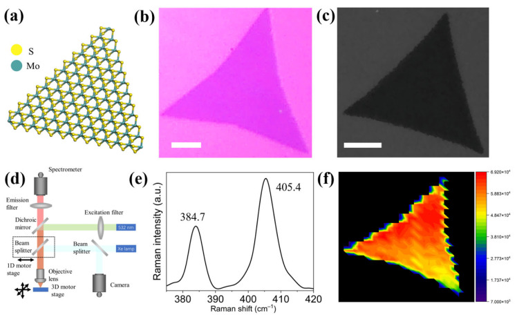
The atomic structure of CVD-synthesized 2H-phase monolayer MoS2 is schematically illustrated in Figure 1a, showing an asymmetry in the horizontal direction. To characterize the morphology of the monolayer MoS2, an equilateral triangle with a smooth side length of ~30 μm can be observed by an optical photograph (Figure 1b), which is in good consistent with the SEM image (Figure 1c). To identify the uniform thickness and optical property of the MoS2, a homemade laser scanning confocal microscope is utilized to study the Raman and PL spectra (Figure 1d). Figure 1e shows the room-temperature Raman spectrum of the MoS2. The two peaks located at 384.7 and 405.4 cm−1 correspond to in-plane mode and out-plane mode of MoS2 crystal, respectively [35]. The peak distance of 20.7 cm−1 agrees well with the character of monolayer MoS2. The universal monolayer region of the MoS2 crystal can also be directly determined by the means of Raman mapping calculated by the intensity of peak (Figure 1f).
Figure 1.
(a) Schematic illustration of the atomic structure of a monolayer MoS2. (b) Optical photograph of a monolayer MoS2. (c) SEM image of a monolayer MoS2. Scalar bar is 10 μm. (d) Structure of the homemade laser scanning confocal microscope. (e) Raman spectrum of the monolayer MoS2. (f) Raman mapping of the monolayer MoS2.
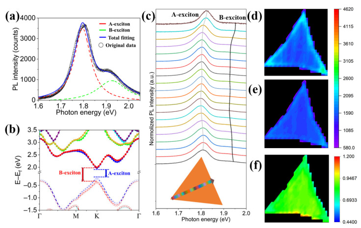
Figure 2a presents a typical PL spectrum of the monolayer MoS2 excited by 532 nm laser at room temperature. The PL spectrum can be perfectly divided into two peaks by the Lorentz formula with R2 = 0.99. The major peak at 1.83 eV and the minor peak at 2.02 eV are raised from the dipole transitions of A-exciton and B-exciton, respectively [35]. To better understand the fundamental formation of the excitons, the electronic structure of monolayer MoS2 is calculated by density functional theory (DFT) with the pseudopotential plane-wave method, as shown in Figure 2b. It is intuitively found that the valence band maximum (VBM) and conduction band minimum (CBM) of the monolayer MoS2 are located at K-point, demonstrating a direct bandgap character. Driven by the strong SOC, both the VBM and CBM split into two bands with opposite spins. The VBM splitting is ~300 meV, which is attributed to the high atomic number of Mo atoms [36,37,38]. The CBM splitting is merely ~15 meV, which is ignored for simplification. Once the monolayer MoS2 is irradiated with a 532 nm laser, the electrons in VBM are excited to CBM and the holes are left in VBM. The electrons in CBM and the holes in VBM with the same spin are attracted by each other to form two bound states, named “exciton”. Generally, the bonded electron−hole pairs with lower and higher energies are called A-exciton and B-exciton, respectively. According to the previous report, the PL properties of monolayer TMDs are dominated by exciton recombination [39]. Figure 2c shows the position-dependent PL spectra of the monolayer MoS2 along the vertice-to-edge direction at 1 μm interval, indicating a red-shift of exciton peaks orienting from center to edge. Accordingly, the center of MoS2 exhibits the maximum intensities for both A-exciton and B-exciton. To further study the excitonic population in MoS2, the PL intensity mapping profiles of A-exciton and B-exciton are shown in Figure 2d,e, respectively. The intensities of A-exciton and B-exciton are both highest at the center area and gradually decrease toward all directions, which is caused by the fringe effect. Figure 2f shows the peak intensity ratio of B-exciton to A-exciton, depicting that the proportion is almost constant throughout the triangle. These results indicate that although the density and energy of exciton state are non-constant under the same pump light, the exciton population is constant. Therefore, to conduct the comparison experiments, the PL spectra must be obtained from the same region of the monolayer MoS2. In this case, the following experiments are all excited from the center of MoS2 triangle.
Figure 2.
(a) A typical PL spectrum of the monolayer MoS2. (b) The SOC-dependent band structure of the monolayer MoS2. The solid and hollow circle represent conduction and valence band, respectively. The energy levels are marked by different colors. (c) The PL spectra with linear scanning from the vertice to edge of the MoS2 triangle. The inset shows the scanning path and the colors of PL spectra indicate the site position. (d–f) The intensity mapping profiles of (d) A-exciton, (e) B-exciton, and (f) intensity ratio of B/A.
3.2. Pump Power Dependent PL Properties
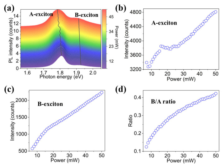
To quantify the population of exciton states in excited monolayer MoS2, the room-temperature PL spectra of the monolayer MoS2 are measured under 532 nm laser with high power evenly ranging from 5 to 50 mW, as shown in Figure 3a. All the PL spectra can be well fitted by the linear superposition of the emission peaks of A-exciton and B-exciton. It can be observed that the energies of A-exciton and B-exciton slightly red-shift with increasing power, which is ascribed to the laser-induced photothermal effect [40]. The peak intensities of A-exciton and B-exciton under different pump powers are shown in Figure 3b,c, respectively, showing a linearly positive correlation between exciton state density and pump power. Figure 3d displays the intensity ratio of B-exciton to A-exciton, which indicates that the B/A intensity ratio is near-linearly and positively related to the pump power. These results suggest that the low-energy A-exciton can spontaneously convert to high-energy B-exciton with increasing pump power in the relatively high region.
Figure 3.
(a) The PL spectra of the monolayer MoS2 pumped by laser with high power ranging from 5 to 50 mW. (b–d) The power-dependent (b) intensity of A-exciton, (c) intensity of B-exciton, and (d) intensity ratio of B/A.
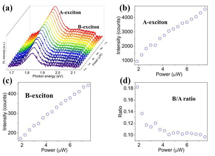
To investigate the variation tendency of exciton state population under low-power pump light, the room-temperature PL spectra of the monolayer MoS2 under 532 nm laser with pump power ranging from 1.875 to 7.85 μW are measured, as shown in Figure 4a. Although the peak intensities around 2.02 eV are much weaker than those around 1.83 eV, all the PL spectra can still be well fitted by two Lorentzian curves assigned to B-exciton and A-exciton located at constant positions. Moreover, both the two peak intensities of A-exciton and B-exciton increase with the increasing pump power (Figure 4b,c). Astonishingly, different from the PL spectra under high pump power, here the intensity ratio of B-exciton to A-exciton nonlinearly decreases while the pump power increases (Figure 4d). Therefore, it can be concluded that the pump light with low power prefers to generate A-exciton but reverses under high power, which has not yet been reported in the previous literature.
Figure 4.
(a) The PL spectra of the monolayer MoS2 under pump light with low power ranging from 1.875 to 7.85 μW. (b,c) The intensity variations of (b) A-exciton and (c) B-exciton under increasing pump power. (d) The ratio variation of B/A intensity ratio under increasing pump power.
3.3. Proposed Mechanism
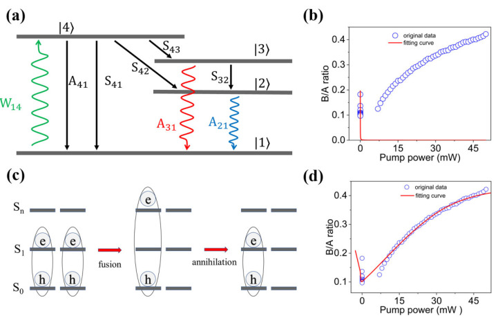
To discuss the abnormal exciton state population in monolayer MoS2 at room temperature, we have firstly developed a simple four-level model, as shown in Figure 5a.
Figure 5.
(a) Schematic diagram of the exciton state population of the monolayer MoS2 during excitation and recombination processes. (b) The theoretical calculation result without EEA-modification. (c) Schematic diagram of exciton−exciton fusion and annihilation processes. (d) The theoretical calculation result with EEA-modification.
When the monolayer MoS2 is irradiated by a 532 nm laser, the electrons in ground state are pumped to high-energy excited state . Then, the metastable A-excitons and B-excitons originated from non-radiation intra-band relaxation and electron−hole Coulomb interaction are generated in state and , respectively. Subsequently, the excitons in state and relax to state through spontaneous radiation, forming the related peaks in PL spectra. Likewise, the electrons in the state relax to the state through spontaneous radiation and non-radiation transition. For simplify, the detailed electron−hole interaction and the non-radiation transition with low possibility are neglected. According to the Purcell effect, the spontaneous emission rate from state to depends on the pump power [41,42]. The population of the four quantum states can be calculated from the phenomenological formula, as described by Equations (1)–(4) [43],
| (1) |
| (2) |
| (3) |
| (4) |
where n represents the total state density, nj represents the state density of excitons and electrons in energy level Ej, Sij, Aij, and Wij represent the non-radiation transition rate, spontaneous emission rate, and stimulated absorption rate from level to , respectively. All the computations and analyses are based on the steady-state assumption that the state densities in the four levels are constant in the whole process, as expressed by . Therefore, the exciton state population can be described by Equation (5),
| (5) |
where IB and IA represent the PL intensities corresponding to A31 and A21, respectively.
Furthermore, a semi-classical model is developed to analyze the dependence of spontaneous emission rate on the pump power by discussing the light−matter interaction. The single-mode electromagnetic wave is expressed in classical form by Equation (6) [44],
| (6) |
where E0 and ω are the amplitude and angular frequency of incident electromagnetic wave, respectively. By solving a time-dependent Schrödinger equation with perturbation method and diploe approximation, the light−matter interaction can be written as Equations (7) and (8) [44],
| (7) |
| (8) |
where V and HA correspond to the interaction Hamiltonian representing the perturbation part and the free particles Hamiltonian, respectively. Since the scale of atom is much smaller than that of photon, the interaction part can be expressed as Equation (9) through dipole approximation [45],
| (9) |
where d is the electric dipole moment, expanded with the eigenstate of HA by Equation (10).
| (10) |
Thus, the transition probability Ƥni(t) can be calculated through perturbation method and rotating approximation, as described by Equation (11),
| (11) |
where ωni is the resonant angular frequency between state and and Ƥni(t) is of positive correlation with pump power (as well as |E0|2). As the difference between ωni and ω is of non-zero value, Ƥni(t) dramatically approaches to zero with calculating the average value. By combining Equations (2) and (8), the B/A intensity ratio has a negative correlation with pump power, as fitted in Figure 5b. The fitting curve displays that the B/A ratio rapidly decreases with increasing pump power and then trends to be gentle. Obviously, the simple four-energy-level model can well describe the variation of exciton state population in low-power region, but is not applicable in high power region, where the mismatch may be attributed to the EEA under high power laser irradiation since the EEA can only be obtained under high photon density.
Subsequently, we have further developed an EEA-modified four-energy-level model to improve the accuracy. For simplifying the calculation, the energy level structure of exciton state is regarded as a three-energy-level model including ground state S0, first excited state S1, and high-order excited state Sn by neglecting other states due to the large detuning between resonance frequency and photon angular frequency, as shown in Figure 5c. In the EEA model, both the state densities of A-exciton and B-exciton existing in state S1 increase with increasing pump power. As the pump power increases to the threshold value, EEA occurs between two nearby A-excitons because the state density of A-exciton is much higher than that of B-exciton. One A-exciton is pumped to high-order excited state with double energy of A-exciton level through energy transfer in exciton fusion process, and another A-exciton is recombined to ground state through non-radiation route. The exciton density nx(r,t) containing annihilation term is proportional to the square of state density, as described by Equation (12) [46],
| (12) |
where r, t, G, D, τx, and CEEA represent the position, time, particle generation rate, exciton diffusion coefficient, single exciton lifetime, and EEA coefficient, respectively. In the case of single point excitation and steady states, there is one more term CEEAnx2 to describe the EEA process than that under low exciton density. The phonon emission induced out-band conversion results in a rapid relaxation, leaving only one exciton after EEA process. Therefore, by considering the EEA process, Equations (2) and (3) can be improved to Equations (13) and (14) [46],
| (13) |
| (14) |
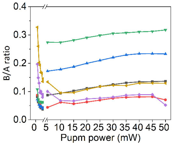
where C2 and C3 correspond to the EEA coefficient in level and , respectively. Since the EEA-modified equations of exciton state population are so complicated that could not be expressed in simplified form, Equation (5) is still used to calculate the exciton state population by ignoring EEA rate. The numerical solution is re-calculated through assigning the certain radiation rate and non-radiation rate obtained from other works, as shown in Figure 5d. Typically, the values of S43 (S42), S32, and A31 are approximated as ~60 fs, 1 ps, and 60 ps, respectively [47,48]. The radiation rate of A41 is a variate related to the total exciton number, which dominates the non-linear exciton population under varying pump power. With increasing pump power, the calculated curve no longer monotonically decreases, and a valley appears. Excitingly, the EEA-modified fitting curve exhibits a high coincidence with experimental data in both lower-power and higher-power region. These results suggest that EEA plays an important role in the spontaneous inversion of exciton states in monolayer MoS2. Excitons are quasi-particles, a kind of Boson. Under low pump power, the exciton number is relatively low, leading to the normal Bose-Einstein distribution of excitons. Since the energy level of A-exciton is lower than B-exciton, the excitons in A-state are more than B-state. Under high pump power, the exciton number is relatively high, and EEA must be considered. With the increasing pump power, the portion of B-excitons increases correspondingly, and the decay of EEA in A-excitons is faster than B-excitons [49,50]. Therefore, it can be concluded that the excitons prefer to exist in a low energy state under low pump power while reverses under high pump power. In addition, the PL spectra of the same sample are measured after keeping in air for 6 months to study the effect of defects since the defect density increases with the increasing time in air through the oxidation of oxygen [48,51,52]. Figure 6 shows the B/A intensity ratio dependent on pump power of 6 sites randomly selected from the same sample. Although the variation tendencies are generally consistent with Figure 5d, the increasing rates in the high-power region are much lower. These results suggest that the exciton population are significantly affected by defects, which should be further studied in future works.
Figure 6.
The variation of the B/A intensity ratio of 6 selected sites from the same sample after keeping in air for 6 months. The B/A ratios raised form different sites are labeled by different colors.
4. Conclusions
In summary, the spontaneous inversion of exciton state population in monolayer MoS2 at room temperature has been observed and discussed. The excitons prefer to exist in low energy state under low pump power, and reverses under high pump power. Since the non-radiation rate keeps constant in the whole excitation−recombination process, the exciton state population can be modulated by pump light through changing the transition probability of spontaneous radiation without other external factors, which is explained by the rate equation and photo-exciton interaction. By combining the relation formula from the rate equations and the final equation from semiclassical theory, the relationship between exciton state population and power of pump light is correlative to the square of transition probability of spontaneous radiation. To make up for the shortcomings of the simple four-energy-level model, EEA theory is introduced in a simplified three-energy-levels system for phenomenologically describing the spontaneous inversion of exciton state population. This work develops a novel all-optical method to modulate exciton population and discusses the EEA process in exciton transition, which provides a possible model to normalize the PL spectrum for SOC studies and contributes to further understanding the light−matter interaction in low-dimensional nanomaterials.
Author Contributions
Conceptualization, Y.F. and J.M.; methodology, Y.F. and Y.L.; software, Z.R. and P.L.; formal analysis, Z.R. and W.L.; investigation, Z.R. and Q.Z.; resources, W.L.; data curation, X.L. ang L.G.; writing—original draft preparation, Z.R., X.L., and L.G.; writing—review and editing, Y.F., J.W., and Y.L.; visualization, Z.R. and W.L.; supervision, Y.F. and J.M.; project administration, Y.F. and J.M.; funding acquisition, Y.F., J.W., and J.M. All authors have read and agreed to the published version of the manuscript.
Institutional Review Board Statement
Not applicable.
Informed Consent Statement
Not applicable.
Data Availability Statement
The data presented in this study are available on request from the corresponding authors.
Conflicts of Interest
The authors declare no conflict of interest.
Funding Statement
This work was funded by the National Key R&D Program of China (2017YFA0304203); the National Natural Science Foundation of China (62020106014, 62175140, 61901249, 92165106, 12104276); PCSIRT (IRT—17R70); 111 project (D18001); the Program for the Outstanding Innovative Teams of Higher Learning Institutions of Shanxi (OIT); the Applied Basic Research Project of Shanxi Province, China (201901D211191, 201901D211188); the Shanxi 1331 KSC; and the collaborative grant by the Russian Foundation for Basic Research and NSF of China (62011530047, 20-53-53025 in the RFBR classification).
Footnotes
Publisher’s Note: MDPI stays neutral with regard to jurisdictional claims in published maps and institutional affiliations.
References
- 1.Sie E.J., McIver J.W., Lee Y.-H., Fu L., Kong J., Gedik N. Valley-selective optical Stark effect in monolayer WS2. Nat. Mater. 2015;14:290–294. doi: 10.1038/nmat4156. [DOI] [PubMed] [Google Scholar]
- 2.Bie Y.-Q., Grosso G., Heuck M., Furchi M.M., Cao Y., Zheng J., Bunandar D., Navarro-Moratalla E., Zhou L., Efetov D.K., et al. A MoTe2-based light-emitting diode and photodetector for silicon photonic integrated circuits. Nat. Nanotechnol. 2017;12:1124–1129. doi: 10.1038/nnano.2017.209. [DOI] [PubMed] [Google Scholar]
- 3.De La Barrera S.C., Sinko M.R., Gopalan D.P., Sivadas N., Seyler K.L., Watanabe K., Taniguchi T., Tsen A.W., Xu X., Xiao D., et al. Tuning Ising superconductivity with layer and spin–orbit coupling in two-dimensional transition-metal dichalcogenides. Nat. Commun. 2018;9:1427. doi: 10.1038/s41467-018-03888-4. [DOI] [PMC free article] [PubMed] [Google Scholar]
- 4.Liang J., Ma H., Wang J., Zhou X., Yu W., Ma C., Wu M., Gao P., Liu K., Yu D. Giant pattern evolution in third-harmonic generation of strained monolayer WS2 at two-photon excitonic resonance. Nano Res. 2020;13:3235–3240. doi: 10.1007/s12274-020-2995-2. [DOI] [Google Scholar]
- 5.Hu G., Hong X., Wang K., Wu J., Xu H.-X., Zhao W., Liu W., Zhang S., Garcia-Vidal F., Wang B., et al. Coherent steering of nonlinear chiral valley photons with a synthetic Au–WS2 metasurface. Nat. Photon. 2019;13:467–472. doi: 10.1038/s41566-019-0399-1. [DOI] [Google Scholar]
- 6.Wu F., Das Sarma S. Collective Excitations of Quantum Anomalous Hall Ferromagnets in Twisted Bilayer Graphene. Phys. Rev. Lett. 2020;124:046403. doi: 10.1103/PhysRevLett.124.046403. [DOI] [PubMed] [Google Scholar]
- 7.Wu L., Cong C., Yang W., Chen Y., Shao Y., Do T.T.H., Wen W., Feng S., Zou C., Zhang H., et al. Observation of strong valley magnetic response in monolayer transition metal dichalcogenide alloys of Mo0.5W0.5Se2 and Mo0.5W0.5Se2/WS2 heterostructures. ACS Nano. 2021;15:8397–8406. doi: 10.1021/acsnano.0c10478. [DOI] [PubMed] [Google Scholar]
- 8.Du L., Hasan T., Castellanos-Gomez A., Liu G.-B., Yao Y., Lau C.N., Sun Z. Engineering symmetry breaking in 2D layered materials. Nat. Rev. Phys. 2021;3:193–206. doi: 10.1038/s42254-020-00276-0. [DOI] [Google Scholar]
- 9.Gao F., Xue H., Yang Z., Lai K., Yu Y., Lin X., Chong Y., Shvets G., Zhang B. Topologically protected refraction of robust kink states in valley photonic crystals. Nat. Phys. 2018;14:140–144. doi: 10.1038/nphys4304. [DOI] [Google Scholar]
- 10.Chen Y.C., Sun M.T. Two-dimensional WS2/MoS2 heterostructures: Properties and applications. Nanoscale. 2021;13:5594–5619. doi: 10.1039/D1NR00455G. [DOI] [PubMed] [Google Scholar]
- 11.Tan C.L., Luo Z.M., Chaturvedi A., Cai Y.Q., Du Y.H., Gong Y., Huang Y., Lai Z.C., Zhang X., Zheng L.R., et al. Preparation of high-hercentage 1T-phase transition metal dichalcogenide nanodots for electrochemical hydrogen evolution. Adv. Mater. 2018;30:1705509. doi: 10.1002/adma.201705509. [DOI] [PubMed] [Google Scholar]
- 12.Jin C.H., Kim J., Utama M.I.B., Regan E.C., Kleemann H., Cai H., Shen Y.X., Shinner M.J., Sengupta A., Watanabe K., et al. Imaging of pure spin-valley diffusion current in WS2-WSe2 heterostructures. Science. 2018;360:893–896. doi: 10.1126/science.aao3503. [DOI] [PubMed] [Google Scholar]
- 13.Samadi M., Sarikhani N., Zirak M., Zhang H., Zhang H.L., Moshfegh A.Z. Group 6 transition metal dichalcogenide nanomaterials: Synthesis, applications and future perspectives. Nanoscale Horiz. 2018;3:90–204. doi: 10.1039/C7NH00137A. [DOI] [PubMed] [Google Scholar]
- 14.Wang X., Li H., Li H., Lin S., Ding W., Zhu X.G., Sheng Z.G., Wang H., Zhu X.B., Sun Y.P. 2D/2D 1T-MoS2/Ti3C2 MXene heterostructure with excellent supercapacitor performance. Adv. Funct. Mater. 2020;30:1910302. [Google Scholar]
- 15.Bhunia H., Pal A.J. Band-edges and band-gap in few-layered transition metal dichalcogenides. J. Phys. D Appl. Phys. 2018;51:215102. doi: 10.1088/1361-6463/aabb90. [DOI] [Google Scholar]
- 16.Roldán R., López-Sancho M.P., Guinea F., Cappelluti E., Silva-Guillén J.A., Ordejón P. Momentum dependence of spin–orbit interaction effects in single-layer and multi-layer transition metal dichalcogenides. 2D Mater. 2014;1:034003. doi: 10.1088/2053-1583/1/3/034003. [DOI] [Google Scholar]
- 17.Kośmider K., Fernández-Rossier J. Electronic properties of the MoS2-WS2 heterojunction. Phys. Rev. B. 2013;87:075451. doi: 10.1103/PhysRevB.87.075451. [DOI] [Google Scholar]
- 18.Dimple N.J., Ahammed R., Rawat A., Mohanta M.K., De Sarkar A. Valley drift and valley current modulation in strained monolayer MoS2. Phys. Rev. B. 2019;100:165413. [Google Scholar]
- 19.Chittari B.L., Chen G., Zhang Y., Wang F., Jung J. Gate-Tunable Topological Flat Bands in Trilayer Graphene Boron-Nitride Moiré Superlattices. Phys. Rev. Lett. 2019;122:016401. doi: 10.1103/PhysRevLett.122.016401. [DOI] [PubMed] [Google Scholar]
- 20.Kang J., Vafek O. Strong Coupling Phases of Partially Filled Twisted Bilayer Graphene Narrow Bands. Phys. Rev. Lett. 2019;122:246401. doi: 10.1103/PhysRevLett.122.246401. [DOI] [PubMed] [Google Scholar]
- 21.Li H., Li S., Naik M.H., Xie J., Li X., Wang J., Regan E., Wang D., Zhao W., Zhao S., et al. Crommie Imaging moire flat bands in three-dimensional reconstructed WSe2/WS2 superlattices. Nat. Mater. 2021;20:945–950. doi: 10.1038/s41563-021-00923-6. [DOI] [PubMed] [Google Scholar]
- 22.Li Z., Wang T., Lu Z., Jin C., Chen Y., Meng Y., Lian Z., Taniguchi T., Watanabe K., Zhang S., et al. Revealing the biexciton and trion-exciton complexes in BN encapsulated WSe2. Nat. Commun. 2018;9:3719. doi: 10.1038/s41467-018-05863-5. [DOI] [PMC free article] [PubMed] [Google Scholar]
- 23.Liu X., Wang Z., Watanabe K., Taniguchi T., Vafek O., Li J.I.A. Tuning electron correlation in magic-angle twisted bilayer graphene using Coulomb screening. Science. 2021;371:1261–1265. doi: 10.1126/science.abb8754. [DOI] [PubMed] [Google Scholar]
- 24.Lundt N., Klembt S., Cherotchenko E., Betzold S., Iff O., Nalitov A., Klaas M., Dietrich C.P., Kavokin A., Hofling S., et al. Room-temperature Tamm-plasmon exciton-polaritons with a WSe2 monolayer. Nat. Commun. 2016;7:13328. doi: 10.1038/ncomms13328. [DOI] [PMC free article] [PubMed] [Google Scholar]
- 25.Cui Q.H., Peng Q., Luo Y., Jiang Y., Yan Y., Wei C., Shuai Z., Sun C., Yao J., Zhao Y.S. Asymmetric photon transport in organic semiconductor nanowires through electrically controlled exciton diffusion. Sci. Adv. 2018;4:eaap9861. doi: 10.1126/sciadv.aap9861. [DOI] [PMC free article] [PubMed] [Google Scholar]
- 26.Goryca M., Li J., Stier A.V., Taniguchi T., Watanabe K., Courtade E., Shree S., Robert C., Urbaszek B., Marie X., et al. Revealing exciton masses and dielectric properties of monolayer semiconductors with high magnetic fields. Nat. Commun. 2019;10:4172. doi: 10.1038/s41467-019-12180-y. [DOI] [PMC free article] [PubMed] [Google Scholar]
- 27.Lo T.W., Zhang Q., Qiu M., Guo X., Meng Y., Zhu Y., Xiao J.J., Jin W., Leung C.W., Lei D. Thermal Redistribution of Exciton Population in Monolayer Transition Metal Dichalcogenides Probed with Plasmon–Exciton Coupling Spectroscopy. ACS Photon. 2019;6:411–421. doi: 10.1021/acsphotonics.8b01349. [DOI] [Google Scholar]
- 28.Yao Q.-F., Cai J., Tong W.-Y., Gong S.-J., Wang J.-Q., Wan X., Duan C.-G., Chu J.H. Manipulation of the large Rashba spin splitting in polar two-dimensional transition-metal dichalcogenides. Phys. Rev. B. 2017;95:165401. doi: 10.1103/PhysRevB.95.165401. [DOI] [Google Scholar]
- 29.Wang L., Nilsson Z.N., Tahir M., Chen H., Sambur J.B. Influence of the Substrate on the Optical and Photo-electrochemical Properties of Monolayer MoS2. ACS Appl. Mater. Interfaces. 2020;12:15034–15042. doi: 10.1021/acsami.9b21230. [DOI] [PubMed] [Google Scholar]
- 30.Luo Y., Shepard G.D., Ardelean J.V., Rhodes D.A., Kim B., Barmak K., Hone J.C., Strauf S. Deterministic coupling of site-controlled quantum emitters in monolayer WSe2 to plasmonic nanocavities. Nat. Nanotechnol. 2018;13:1137–1142. doi: 10.1038/s41565-018-0275-z. [DOI] [PubMed] [Google Scholar]
- 31.Hien N.D., Nguyen C.V., Hieu N.N., Kubakaddi S.S., Duque C.A., Mora-Ramos M.E., Dinh L., Bich T.N., Phuc H.V. Magneto-optical transport properties of monolayer transition metal dichalcogenides. Phys. Rev. B. 2020;101:045424. doi: 10.1103/PhysRevB.101.045424. [DOI] [Google Scholar]
- 32.Shimazaki Y., Schwartz I., Watanabe K., Taniguchi T., Kroner M., Imamoğlu A. Strongly correlated electrons and hybrid excitons in a moiré heterostructure. Nature. 2020;580:472–477. doi: 10.1038/s41586-020-2191-2. [DOI] [PubMed] [Google Scholar]
- 33.Xue D.-J., Hou Y., Liu S.-C., Wei M., Chen B., Huang Z., Li Z., Sun B., Proppe A.H., Dong Y., et al. Regulating strain in perovskite thin films through charge-transport layers. Nat. Commun. 2020;11:1514. doi: 10.1038/s41467-020-15338-1. [DOI] [PMC free article] [PubMed] [Google Scholar]
- 34.Yang J.C., Kim J.-O., Oh J., Kwon S.Y., Sim J.Y., Kim D.W., Choi H.B., Park S. Microstructured Porous Pyramid-Based Ultrahigh Sensitive Pressure Sensor Insensitive to Strain and Temperature. ACS Appl. Mater. Interfaces. 2019;11:19472–19480. doi: 10.1021/acsami.9b03261. [DOI] [PubMed] [Google Scholar]
- 35.Buscema M., Steele G.A., van der Zant H.S.J., Castellanos-Gomez A. The effect of the substrate on the Raman and photoluminescence emission of single-layer MoS2. Nano Res. 2015;7:561–571. doi: 10.1007/s12274-014-0424-0. [DOI] [Google Scholar]
- 36.Kadantsev E.S., Hawrylak P. Electronic structure of a single MoS2 monolayer. Solid State Commun. 2012;152:909–913. doi: 10.1016/j.ssc.2012.02.005. [DOI] [Google Scholar]
- 37.Li T., Gui Y., Zhao W., Tang C., Dong X. Palladium modified MoS2 monolayer for adsorption and scavenging of SF6 decomposition products: A DFT study. Phys. E: Low-Dimensional Syst. Nanostructures. 2020;123:114178. doi: 10.1016/j.physe.2020.114178. [DOI] [Google Scholar]
- 38.Akhtar P., Khan M.J.I., Kanwal Z., Ramay S.M., Mahmood A., Saleem M. Ab-initio and experimental investigations on Au incorporated MoS2 for electronic and optical response. J. Alloy. Compd. 2021;877:160244. doi: 10.1016/j.jallcom.2021.160244. [DOI] [Google Scholar]
- 39.Yuan Y., Chen M., Yang S., Shen X., Liu Y., Cao D. Exciton recombination mechanisms in solution grown single crystalline CsPbBr3 perovskite. J. Lumin- 2020;226:117471. doi: 10.1016/j.jlumin.2020.117471. [DOI] [Google Scholar]
- 40.Luo H., Li X., Zhao Y., Yang R., Bao L., Hao Y., Gao Y.-N., Shi N.N., Guo Y., Liu G., et al. Zhou Simultaneous generation of direct- and indirect-gap photoluminescence in multilayer MoS2 bubbles. Phys. Rev. Mater. 2020;4:074006. doi: 10.1103/PhysRevMaterials.4.074006. [DOI] [Google Scholar]
- 41.Cai Y.Y., Liu J.G., Tauzin L.J., Huang D., Sung E., Zhang H., Joplin A., Chang W.S., Nordlander P., Link S. Photoluminescence of Gold Nanorods: Purcell Effect Enhanced Emission from Hot Carriers. ACS Nano. 2018;12:976–985. doi: 10.1021/acsnano.7b07402. [DOI] [PubMed] [Google Scholar]
- 42.An K., Feld M.S. Semiclassical four-level single-atom laser. Phys. Rev. A. 1997;56:1662–1665. doi: 10.1103/PhysRevA.56.1662. [DOI] [Google Scholar]
- 43.Al-Nashy B., Abdullah M., Al-Shatravi A.G., Al-Khursan A.H. Lasing without population inversion in a four-level Y-type configuration in double quantum dot system. Pramana. 2018;91:74. doi: 10.1007/s12043-018-1646-6. [DOI] [Google Scholar]
- 44.Willatzen M., Wang Z.L. Theory of contact electrification: Optical transitions in two-level systems. Nano Energy. 2018;52:517–523. doi: 10.1016/j.nanoen.2018.08.015. [DOI] [Google Scholar]
- 45.Rzazewski K., Boyd R.W. Equivalence of interaction Hamiltonians in the electric dipole approximation. J. Mod. Opt. 2004;51:1137–1147. doi: 10.1080/09500340408230412. [DOI] [Google Scholar]
- 46.Uddin S.Z., Rabani E., Javey A. Universal Inverse Scaling of Exciton–Exciton Annihilation Coefficient with Exciton Lifetime. Nano Lett. 2021;21:424–429. doi: 10.1021/acs.nanolett.0c03820. [DOI] [PubMed] [Google Scholar]
- 47.Dong N., Li Y., Zhang S., McEvoy N., Gatensby R., Duesberg G.S., Wang J. Saturation of Two-Photon Absorption in Layered Transition Metal Dichalcogenides: Experiment and Theory. ACS Photon. 2018;5:1558–1565. doi: 10.1021/acsphotonics.8b00010. [DOI] [Google Scholar]
- 48.McCreary K.M., Hanbicki A.T., Sivaram S.V., Jonker B.T. A- and B-exciton photoluminescence intensity ratio as a measure of sample quality for transition metal dichalcogenide monolayers. APL Mater. 2018;6:111106. doi: 10.1063/1.5053699. [DOI] [Google Scholar]
- 49.Sun D., Rao Y., Reider G.A., Chen G., You Y., Brézin L., Harutyunyan A.R., Heinz T.F. Observation of Rapid Exciton–Exciton Annihilation in Monolayer Molybdenum Disulfide. Nano Lett. 2014;14:5625–5629. doi: 10.1021/nl5021975. [DOI] [PubMed] [Google Scholar]
- 50.Lee K.J., Xin W., Guo C. Annihilation mechanism of excitons in a MoS2 monolayer through direct Forster-type energy transfer and multistep diffusion. Phys. Rev. B. 2020;101:195407. doi: 10.1103/PhysRevB.101.195407. [DOI] [Google Scholar]
- 51.He Z., Guo Z., Zhong X., Chen X., Xue J., Wang X., Chen Y. Spectroscopic investigation of defects mediated oxidization of single-layer MoS2. Sci. China Technol. Sci. 2021;64:611–619. doi: 10.1007/s11431-020-1593-4. [DOI] [Google Scholar]
- 52.Fujisawa K., Carvalho B.R., Zhang T., Perea-López N., Lin Z., Carozo V., Ramos S.L.L.M., Kahn E., Bolotsky A., Liu H., et al. Quantification and Healing of Defects in Atomically Thin Molybdenum Disulfide: Beyond the Controlled Creation of Atomic Defects. ACS Nano. 2021;15:9658–9669. doi: 10.1021/acsnano.0c10897. [DOI] [PubMed] [Google Scholar]
Associated Data
This section collects any data citations, data availability statements, or supplementary materials included in this article.
Data Availability Statement
The data presented in this study are available on request from the corresponding authors.


