

Abstract
Inverting a semiconducting channel is the basis of all field-effect transistors. In silicon-based metal-oxide-semiconductor field-effect transistors (MOSFETs), a gate dielectric mediates this inversion. Access to inversion layers may be granted by interfacing ultrathin low-dimensional semiconductors in heterojunctions to advance device down-scaling. Here we demonstrate that monolayer molybdenum disulfide (MoS2) can directly invert a single-walled semiconducting carbon nanotube (SWCNT) transistor channel without the need for a gate dielectric. We fabricate and study this atomically thin one-dimensional/two-dimensional (1D/2D) van der Waals heterojunction and employ it as the gate of a 1D heterojunction field-effect transistor (1D-HFET) channel. Gate control is based on modulating the conductance through the channel by forming a lateral p–n junction within the CNT itself. In addition, we observe a region of operation exhibiting a negative static resistance after significant gate tunneling current passes through the junction. Technology computer-aided design (TCAD) simulations confirm the role of minority carrier drift-diffusion in enabling this behavior. The resulting van der Waals transistor architecture thus has the dual characteristics of both field-effect and tunneling transistors, and it advances the downscaling of heterostructures beyond the limits of dangling bonds and epitaxial constraints faced by III–V semiconductors.
Keywords: mixed-dimensional, heterojunction, carbon nanotube, MoS2, van der Waals heterostructure, junction field-effect transistor, negative resistance
Graphical Abstract

Inverting a transistor channel with the field effect modulates its conductance and gives rise to metal-oxide-semiconductor field-effect transistors (MOSFETs), which are the most ubiquitous electronic devices manufactured today. The MOSFET incorporates an electrically insulating gate dielectric to mediate electrostatic inversion in the transistor channel. However, the scaling of gate dielectrics is limited by gate tunneling currents that must be kept below 10 A cm−2 in most circuit applications.1,2 Improvements in MOSFET electrostatics to achieve the desired channel length scaling are being explored, among others, through 1D nanowire, gate-all-around architectures.3,4 In this work, we explore field-effect transistors based on transport at the mixed-dimensional heterojunction (MDHJ) interface between a 2D gate, in the form of monolayer MoS2, and a 1D channel, in the form of a semiconducting carbon nanotube (CNT). The conduction-band discontinuity formed at this heterojunction acts as a barrier to tunneling transport in reverse bias while mediating inversion of the underlying CNT channel. In this way, such devices have features in common with gallium arsenide–aluminum gallium arsenide (GaAs–AlGaAs) high-electron-mobility transistors (HEMTs) while enabling the fabrication of a 1D channel with high-quality van der Waals interfaces that do not require lattice matching and that mitigate issues associated with trap states introduced by dangling bonds at conventional gate-oxide interfaces in bulk materials.
Since the 1970s, it has been known that highly doped abrupt p–n heterojunctions support inversion layers at their material interface.5,6 When the p–n heterojunction is reverse-biased, a minimum inversion voltage, Vi, can be defined, for which this layer always exists
| (1) |
where k is the Boltzmann constant, T is the temperature, q is the electronic charge, N1 and N2 are the respective doping levels of the two materials, and A is a material constant dependent on the exact band offset at the junction, ΔEi = (χ1 + Eg1/2) – (χ2 + Eg2/2), where χ1 and χ2 are the respective electron affinities and Eg1 and Eg2 are the respective band gaps. The condition for the formation of an inversion layer is then determined by ΔEi < 0 eV.6 Modulation doping of this kind has been utilized for decades in III–V heterojunctions to form modulation-doped HEMTs for high-frequency switching and power electronics applications.7,8 However, these material systems rely on the lattice-matched epitaxial growth of bulk semiconductors to provide the necessary interface quality in these transistor applications with lattice-matching requirements at the heterointerfaces.
MDHJs are an emerging class of nanoscale devices with many intriguing electrical and optical properties.9–13 Stacked van der Waals heterojunctions allow for the flexible fabrication of such structures free of constraints imposed by heteroepitaxy14–17 and of the dangling bonds characteristic of many heterointerfaces.18–28 Synthetic van der Waals materials are therefore ideal candidates for realizing atomically abrupt highly doped p–n heterojunctions. Modulation-doped layers were already observed in multilayer heterostructures of MoS2 and tungsten diselenide (WSe2), where the estimated inversion layer thickness was <2 nm,29 and were recently employed to create remotely doped 2D/2D field-effect transistors with improved electron mobilities due to reduced dopant-related scattering.30 Solid-state tungsten oxyselenide has also been recently shown to efficiently dope graphene through direct charge transfer.31 Individual 1D metallic single-walled carbon nanotubes (SWCNTs), in turn, have been observed to electronically couple to 2D semiconductors in vertical van der Waals heterojunctions.32–36 Meanwhile, a recent report has shown that an MDHJ consisting of a semiconducting multiwalled CNT and multilayer MoS2 exhibits gate-tunable band-to-band tunneling (BTBT) in reverse bias.37 A wrap-around gate architecture utilizing monolayer n-type MoS2 as the gate for a p-type SWCNT channel is therefore expected to be electrostatically effective in creating strong inversion, as the electronic band gap of MoS2 increases from 1.2 to >2 eV in the monolayer limit, creating large conduction and valence band discontinuities at the material interface.
Here we exploit such heterojunctions to create a 1D depletion-mode heterostructure field-effect transistor (1D-HFET) in which the formation of the inversion layer shuts the device off. Inverting the CNT with the MoS2 gate creates a voltage-controlled migrating lateral p–n junction inside of the nanotube channel itself as the device is biased deeper into inversion. The n-type layer that begins to form at the source extends toward the drain and controls the flow of drain current by forming a reverse-biased p–n homojunction at the source terminal. At high gate-to-channel reverse biases, the gate begins to leak through BTBT. This injects holes into the inverted electron channel in the nanotube, and they diffuse to the source and drain terminals, producing a partitioned current flowing out of the source and drain, even at Vds > 0 V.
RESULTS AND DISCUSSION
Atomic-Scale 1D/2D Heterojunction Fabrication and Characterization.
The 1D-HFET device is shown in Figure 1a. The constituent n-type MoS2 and p-type SWCNT of the MDHJ are separately synthesized by distinct chemical vapor deposition (CVD) processes;38,39 these steps are described in detail in the Methods and in Supporting Figure 1. We interface the two materials with a site-non-specific wet-transfer method, similar to a previously reported approach for 2D materials on SiO2,40 where we deposit the MoS2 monolayers on top of the nanotubes on their native growth substrate. Because of the dense areal coverage of the MoS2 flakes and the relatively long span of the individual nanotubes, this can yield several junctions per single nanotube. A closer look at a formed junction is presented in the electrostatic force microscopy (EFM) map in Figure 1b. Under no biasing, the as-formed MDHJ shows strong contrast from the underlying SiO2 substrate and a slight variation in the phase offset between the MoS2 flake area and the overlap area with the SWCNT, similar in magnitude to those observed in EFM for MoS2/pentacene heterojunctions,41 suggesting a localized change in the surface potential due to charge transfer at the interface. The atomic force microscopy (AFM) height maps in Supporting Figure 2 reveal that the SWCNT lifts the edge of the MoS2 flake off the substrate by several nanometers while the monolayer semiconductor wraps around the nanotube, creating a protruding ridge on the surface. Figure 1c is a representative scanning electron micrograph (SEM) showing the formed MDHJs following the transfer process, with more examples presented in Supporting Figure 3. When compared with typical 2D/2D van der Waals heterojunctions, which can be thousands of squared microns in area, for example, WSe2/MoS2,42 our 1D/2D contact areas are five orders of magnitude smaller, with an average overlap area of 0.018 μm2, as extracted across MDHJs from three different CNT growth substrates.
Figure 1.

Mixed-dimensional 1D/2D van der Waals heterojunction platform. (a) Illustration of the van der Waals 1D-HFET architecture with the three electrical terminals outlined. (b) EFM phase map of an as-made MDHJ at no applied bias across the device, showing the relative change of surface potential across the junction. (c) Large-area SEM demonstrating the typical morphology of the junction areas following the transfer procedure. In many cases, a single nanotube is contacted with multiple MoS2 flakes. (d) Raman spectra of monolayer MoS2 on the bare flake (blue) and in the MDHJ region (green). (e) Raman spectra of the SWCNT on the bare nanotube (purple) and in the MDHJ region (green). (f) Photoluminescence spectra of monolayer MoS2 from a bare flake region (red) and from the MDHJ region (green).
Figure 1d shows the change to the Raman signal of the as-grown monolayer MoS2 (blue) in the region of the MDHJ interface (green). In the heterojunction area, both the in-plane (E′) and out-of-plane () Raman modes of MoS2 experience significant intensity quenching. In addition, the 2LA(M) mode at ~450 cm−1 is also substantially quenched. The intensity decrease is expected as the dielectric screening environment of MoS2 at the MDHJ changes significantly, and similar Raman quenching has also been observed in other layered semiconductor heterojunctions.16,23,29 The positions of both characteristic peaks shift from 383.8 to 384.3 cm−1 for the E′ mode and from 403.0 to 403.3 cm−1 for the mode. The upshift in both peaks has previously been associated with electron withdrawal from MoS2.43 This is in agreement with the expected charge transfer occurring at the formed p–n heterojunction interface, which has also recently been indirectly probed with electrical measurements in multilayer MoS2/multiwall CNT junctions.37
In the same vein, Figure 1e shows the Raman spectrum of the G band of a semiconducting SWCNT.44 Relative to the as-synthesized SWCNT (purple), the peak intensity in the MDHJ region (green) decreases substantially, accompanied by noticeable broadening and an upshift of the peak position from 1593.1 to 1595.1 cm−1. This shift of the G band has previously been reported for the noncovalent functionalization of SWCNTs with donor molecules.45 The upshift in the peak position following electron acceptance in SWCNTs is theoretically expected for donor concentrations of up to ~1013 cm−2, beyond which the G peak begins to downshift.46 In our case, the unidirectional 2 cm−1 upshift is thus likely caused by direct electron transfer from the MoS2 to the CNT. This strong interlayer charge transfer in thin van der Waals materials has recently been shown to also invert n-type MoS2 to p-type when interfaced in a p–n heterojunction with WSe2.47
Figure 1f shows the photoluminescence (PL) spectrum of monolayer MoS2 taken from the same flake in the non-overlapped area (orange) and from the MDHJ area (green). A notable decrease in the PL yield is observed in the heterojunction-containing area, as significant nonradiative recombination now occurs due to charge transfer at the junction. This has also been reported for other MDHJs containing layered semiconductors or SWCNTs.9,11,26,30,48 A small downshift to the direct-recombination A exciton energy is also observed (from 1.85 to 1.83 eV), whereas the integrated contribution of the spin–orbit split B exciton is more significant in the heterojunction region. This suggests a more complex interplay between photogenerated excitons and built-in charges at the junction, which warrants a dedicated study. We present additional Raman and PL data sets from other MDHJ samples, including peak fitting and discussion, in Supporting Figure 4.
Mixed-Dimensional van der Waals p–n Diode.
We proceed with the discussion of the measured temperature-dependent I–V characteristics of the atomic-scale p–n MDHJ diode (illustrated in Figure 2a and shown in the colored SEM image in Figure 2b). Figure 2c presents the two-terminal I–V characteristics of the diode taken at various temperatures between 300 and 20 K. Positive (negative) voltages signify nominal forward (reverse)-bias functionality; that is, the CNT is at a high potential relative to the MoS2 in forward bias. The band alignment at the hybrid 1D/2D heterojunction is expected to produce a Type I heterojunction, that is, a straddling gap, which was also recently reported in a coaxial 1D CNT–MoS2 heterostructure with a boron nitride spacer49 and in multiwalled CNT/multilayer MoS2 devices.37 Note that the van der Waals gap is explicitly omitted here. The electron affinities of the two materials (χMoS2 = 4.2 eV, χCNT = 4.3 to 4.5 eV) and the electronic band gaps (Eg,MoS2 = 2.15 eV, Eg,CNT ≈ 0.6 eV) result in significant conduction and valence band discontinuities (ΔEC and ΔEV, respectively), forming inversion layers at the interface in a manner analogous to GaAs–AlGaAs p–n heterojunctions.50 Because the materials used here are extremely thin, the high electric field established by applying an external voltage will heavily bend the bands at the 1D/2D interface, strongly modulating the charge transport across the heterojunction. Supporting Figure 5 shows expected heterojunction band diagrams before layers are contacted and in equilibrium without external bias.
Figure 2.
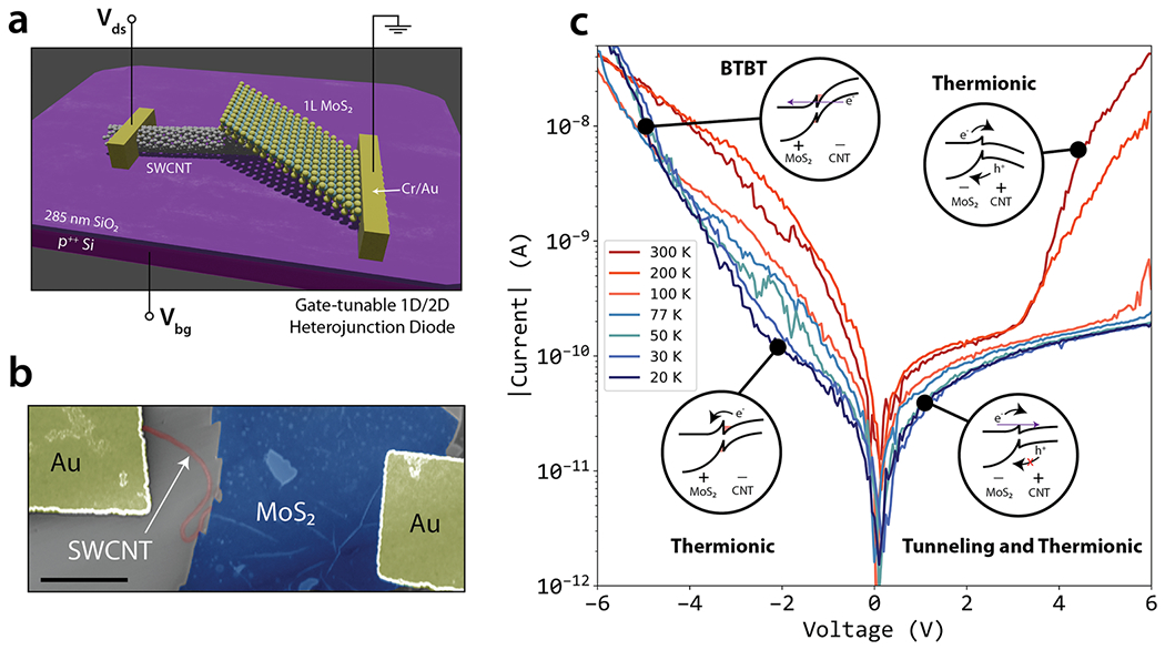
Temperature-dependent I–V characteristics of the 1D/2D p–n heterojunction diode. (a) Sketch of the two-terminal atomic-scale diode. (b) False-colored SEM of the tested device. Scale bar, 2 μm. (c) Temperature-dependent I–V characteristics of the SWCNT–MoS2 device measured at Vbg = 0 V, with the bias conventions illustrated in the insets on the plot. The band diagram insets conceptualize the transport behavior across the heterojunction in each region of the sweep.
In forward bias, the device current increases rapidly at first when V < 1 V, dominated by low-bias direct tunneling. Because of the large band gap of the MoS2 monolayer, thermionic hole transport from the CNT to the MoS2 is limited in this region. As the voltage on the CNT is increased, a weakly temperature-dependent plateau of ~3 V is traversed until significant thermionic hole conduction begins to take over at room temperature, as the CNT bands are bent down by the strong electric field. Because these are thermally generated carriers, their contribution is strongly suppressed at cryogenic temperatures, extending the voltage plateau to >6 V below 77 K. In reverse bias, the device is initially in a strong thermionic regime, where the current can be modulated by over two orders of magnitude between room temperature and 20 K. This is due to minority carrier transport across the interface barrier from the CNT to the MoS2, which is heavily dependent on thermal activation. Because the depletion region in this atomically thin p–n junction is vanishingly thin,51 any minority carriers generated within the diffusion length of the 1D/2D interface will be swept across the vertical space-charge region, resulting in substantial reverse-bias saturation currents. At high temperatures, the contributions of this generation current and that of BTBT to the total current are convoluted together. At 20 K, it is more clearly observed that BTBT begins to dominate transport in reverse bias at approximately −2 V. At this point, tunneling of electrons from the valence band of the CNT to the conduction band of the MoS2 begins to dominate carrier transport across the junction, and it is largely temperature-independent.37 This tunneling breakdown is reversible and indicates a Zener-like mechanism, as the critical voltage52 necessary for BTBT here is <4Eg/q = 5.16 V, when considering the lower band gap of the CNT at Eg ≈ 0.6 eV. We remark here that device-to-device variation during fabrication can result in these regimes existing over different voltage ranges, although the key features of BTBT and the reverse-bias generation current persist. (See the Supporting Figure 6 for I–V data of six more devices with different channel lengths.) We suspect that much of this variation is the result of recombination–generation centers introduced at the van der Waals interface during the wet-transfer procedure.
The I–V response of the MDHJ diodes changes considerably when Vbg is applied to control the carrier density in the heterostructure. As seen from the linear and semilog scale plots of another device (Figure 3a,b), increasing Vbg suppresses the junction conductance in reverse-bias, as was also found for multiwall CNT/multilayer MoS2 devices.37 Interestingly, this trend is opposite to that seen for ensemble SWCNT–MoS2 networks,53 suggesting that junction geometry is the governing factor for individual MDHJ devices. The observed suppression of reverse-bias conductance may thus be attributed to an increased doping offset between the bare CNT portion and the part of the nanotube that is covered by the MoS2 flake. As shown in the Raman results, the CNT readily accepts electrons from the MoS2 and becomes n-doped. With increasing positive Vbg, this inversion deepens in the covered CNT region, developing a more rectifying p–n homojunction within the CNT itself. This raises the diode rectification ratio from 9.5 at Vbg = 0 V to 3.4 × 10⁴ at Vbg = 10 V. Eventually, as the CNT fully inverts at very high positive back-gate voltages, an effective n–n+ heterojunction is formed,53 and the diode rectification ratio decreases. This forward-bias rectification effect is more pronounced for monolayer MoS2 flakes than multilayer flakes37 due to reduced electrostatic screening, granting the monolayer-based architecture an advantage in terms of the conductance tunability. The negative Vbg rectification trend is explained analogously; in this case, a p–p+ heterojunction forms as the MoS2 is depleted by the highly negative gate voltage, forming a backward-rectifying junction with the enhanced p-type CNT.37
Figure 3.

Gate tunability of the MDHJ diode. (a,b) Gate tunability of the diode I–V characteristics on linear and semilog scales, respectively. The colors correspond to the magnitude of the applied back-gate bias mapped to the color bars next to the panels. The inset of panel a shows the rectification ratio extracted at Vds = ±5 V as a function of Vbg. (c) Gate curve of the p–n heterojunction (Lch = 4 μm), exhibiting an antiambipolar response and two distinct off-states. Inset shows the back-gate transfer curve of a SWCNT on the same chip.
The back-gated transfer characteristics of the individual junction devices demonstrate a clear antiambipolar window behavior that was previously also observed in ensemble SWCNT–MoS2 junctions18,53 and was recently employed to make proof-of-concept 1D/2D tunneling FETs.37 The off states seen in the transfer curve correspond to transition regions on either side of the back-gate-dependent n–n+/p–p+ diode formation. The CNT-controlled majority-hole side of the gate sweep dominates the device response at negative Vbg, likely due to the easier depletion of the thinner MoS2 monolayer by the back gate. Additional evidence of electron transfer between the MoS2 and the CNT can be obtained from changes to the secondary electron yield, that is, work function contrast in the SEM. In some devices, we observed the MoS2 areas near the CNT junction turning significantly darker than the rest of the flake under the same imaging conditions. (See Supporting Figure 7.) In the following sections, we focus on utilizing the reverse-bias regime of the 1D/2D heterojunction, which causes inversion in the CNT to create HEMT-like transistor action.
1D Heterojunction Field-Effect Transistor.
As shown in Figure 4a, reverse-biasing the gate junction beyond the threshold voltage, Vi, allows for an n-type region to form in the nanotube. We note that in the case of Vgs ≈ 0 V, for a typical drain bias of Vds = 1 V, an inverted n-type region already exists at the drain due to minority carrier injection at the gate–drain junction,54 but it is not sufficient to turn the device off, resulting in depletion-mode transistor behavior. With increasing positive top-gate voltage, the gate heterojunction becomes more reverse-biased, and the n-type layer extends from the drain to the source, resulting in a reduced Ids. The band diagram in Figure 4b shows how the inversion layer at the interface of the van der Waals MDHJ forms under reverse bias. The native electron doping levels for CVD-synthesized MoS2 are on the order of 0.13 nm−2,55 whereas the induced carrier density between MoS2 and an individual CNT of diameter ~1.2 nm has been calculated at 0.39 nm−1.37 The diameters of SWCNTs used here are <2 nm, resulting in strong inversion at gate voltages exceeding Vi. Moreover, utilizing monolayer MoS2 with its larger band gap increases the band offsets at the junction interface, making single-layer 2D semiconductor gates more favorable candidates for mediating inversion than their lower band gap multilayer counterparts.
Figure 4.

Mixed-dimensional heterojunction inversion field effect. (a) Illustration of the 1D-HFET device architecture when the gate junction is reverse-biased past Vi. An inversion layer begins to form in the carbon nanotube, which renders holes minority carriers in the device channel. (b) Associated band diagram of the heterojunction in reverse bias, visualizing the formation of the inversion layer. (c) TCAD-simulated space-charge heatmaps showing the formation of the p–n homojunction in the CNT channel. (d) TCAD-simulated top-gate (Igs) and drain (Id) currents as a function of the applied gate bias. Note that Id here is explicitly current into the drain and not exclusively Ids. (e) Experimentally recorded Igs and Id traces, showing the shifted onset of channel shut-off in the real device.
Figure 4c presents the TCAD-simulated space-charge distributions in the 1D-HFET device when the gate heterojunction is in nominal reverse bias, that is, Vgs > 0 V. As seen in the plots, inversion occurs in both the CNT channel and the MoS2 gate due to the conduction and valence band discontinuities. This creates gate leakage characteristics that are the same as the I–V response of the two-terminal diode in Figures 2 and 3. (See the experimental Igs–Vgs traces in Supporting Figure 8.) Figure 4d shows the TCAD-simulated drain (Id) and top-gate (Igs) currents as a function of the voltage applied to the MoS2 gate. Simulations predict that the channel conduction in the CNT may be reduced by eight orders of magnitude before significant gate leakage currents flow through the 1D/2D gate junction. The formation of the internal p–n–p homojunction inside the CNT is also independent of current flow through the gate heterojunction. (See TCAD simulations with BTBT disabled in Supporting Figure 9.) This inversion-facilitated field-effect window is subsequently followed by a region of negative current flow into the drain when gate leakage becomes significant. The corresponding measured experimental performance is shown in Figure 4e. In contrast with the simulated results, the drain current characteristic has a much larger threshold voltage. As a result, significant tunneling current flows before the drain current can be fully turned off. In Supporting Figure 10, we show TCAD simulations that demonstrate how the electrostatics of the junction interface strongly affect the threshold voltage. As expected, a more conformal gate wrapping of the CNT leads to a much shorter screening length and threshold voltage. The tent-like structure achieved here experimentally likely introduces stray fields that require higher voltages to fully invert the CNT. (See the data from another device in Supporting Figure 11.) Coaxial wrapping in 1D van der Waals diodes49,56 may be an attractive solution to eventually quench the tunneling current through appropriate work function and band-gap engineering.
1D-HFET Behavior for Vgs ≫ Vds.
This condition, such that BTBT occurs at the gate, should be avoided in normal device operation. However, it is of interest to examine how the device behaves in this regime. Figure 5a shows linear-scale 1D-HFET Id versus Vgs curves recorded at Vds values of 0.1, 0.5, and 1.0 V. After inversion occurs and the drain current fully switches off, continuing the gate sweep to high voltages results in the drain current flowing out of the drain (or the current into the drain turning negative). This is marked by the blue negative static resistance region on the plot in Figure 5a, where more current flows out of the drain for a lower Vds (see also the semilog scale plots in Figure 5b), with the gate leakage current now flowing from the gate to the drain, even though Vds > 0 V, because in this case, Vgd > 0 V. In this bias regime, electrons from the valence band of the CNT tunnel into the conduction band of the MoS2. This constitutes the high positive current flow into the gate terminal. In MOSFETs with ultrathin gate oxides, this large gate-to-channel current partitions into source and drain currents.57–59 The notch of the gate leakage current trace in our devices is also observed to shift accordingly with the applied Vds (see Supporting Figure 7), as expected from the drain-dominated partitioning model.59 In the ultrathin body 1D-HFET, a consequence of the BTBT action localized at the gate junction is the injection of a high concentration of holes into the middle of the inverted CNT channel, which transport by both drift and diffusion to both the source and the drain.
Figure 5.

Operation of the 1D-HFET at high gate biases. (a) 1D-HFET transfer curves taken at different Vds biases. Red circles mark the crossing point of Id from positive to negative, where the device enters the negative static resistance region colored in blue. The device is shown in the image in the inset. (b) Same curves shown on a semilog scale. Note the reversed dependence of the current magnitude on the Vds magnitude at high positive gate voltages. (c) Output characteristics of the 1D-HFET at increasing MoS2 gate biases. For higher Vgs values, the device characteristics migrate deeper into the fourth quadrant of the I–V plane. (d) TCAD-simulated longitudinal electric-field distribution in the carbon nanotube after gate tunneling (Vgs = 22 V), showing the migration of charge carriers away from the center of the channel, where the CNT–MoS2 gate junction is. (e) TCAD-simulated gate, drain, and source current traces as a function of Vgs. The gate current due to electron tunneling is balanced by hole current flowing out of the source and out of the drain.
In Figure 5d, the TCAD-generated electric-field vector maps in the CNT channel at Vgs = 22 V show current flow out both the source and drain terminals. In addition, in Figure 5e, we show the TCAD-simulated gate, drain, and source characteristics as a function of the applied Vgs. As Id decreases initially before gate breakdown, the source current (which is of opposite sign to the drain current) is tracking Id. When the gate tunneling current increases, the drain and source currents begin to be dominated by Igs, with an observed increase in the source current, which also generates the observed negative resistance at the drain.
We remark here on the possible future routes of engineering this hybrid dimensional material system to utilize the modulation-doped 1D-HFET devices for circuit applications. As shown recently in remotely doped 2D/2D van der Waals heterostructures, modulation doping by direct charge transfer can improve the carrier mobility in quantum-confined transistor channels through the mitigation of charged impurity scattering.30 Thus 1D/2D heterostructures may be well-positioned to enable the fabrication of high-mobility 1D transistors in the atomic limit. Ultimately, the fabrication of enhancement-mode devices is necessary, which might be achieved through the specialized contact engineering of CNTs60,61 or the utilization of chemically doped 2D gates,30 such that the CNT channel is normally off at Vgs = 0 V. In addition, further transport studies need to be performed to determine the nature of the formed 1D electron gas and to investigate the role of charged impurity scattering from the MoS2 monolayer on carriers in the CNT channel.
CONCLUSIONS
In summary, we have reported an atomically thin van der Waals MDHJ diode whose electronic properties allow for the creation of a prototype dielectric-less transistor on the nanoscale. In many respects, the 1D-HFET is a 1D version of the standard HEMT device structure, taking full advantage of 1D/2D heterojunctions in the atomic limit. However, full control and understanding of the mechanisms of gate tunneling and junction quantum capacitance in these devices must still be explored. Moreover, future spectroscopic studies should focus on elucidating the nature of the charge transfer between 2D semiconductors and CNTs to allow for more controlled engineering of device physics at these MDHJs.
METHODS
Carbon Nanotube Synthesis.
SWCNTs were grown by alcohol catalytic chemical vapor deposition (ACCVD) in a quartz tube furnace with a 28 mm inner tube diameter. Cobalt thin films (~4 nm) were deposited on thermally oxidized (285 nm SiO2) p++ silicon substrates in an Angstrom Ultra High Vacuum EvoVac electron beam evaporator at a chamber pressure of ~2 × 10− mbar. The substrates were partially masked with Kapton tape to define multiple Co areas on the chip. Prior to CNT growth, the tape was taken off, and the substrates were annealed for 10 min at 750 °C in air and for another 10 min under flowing Ar gas (120 sccm). CNT growth occurred at a temperature of 890 °C with a H2/Ar gas flow (8.7 and 40 sccm, respectively) through an ethanol gas bubbler submerged in an ice bath. The total growth time was 60 min, after which the ethanol bubbler was diverted from the gas flow and the furnace was cooled to room temperature in ~15 min by fan.
Single-Layer MoS2 Synthesis.
Solutions of sodium cholate growth promoter (10 mg mL−1) and ammonium heptamolybdate (11 mg mL−) were spun onto precleaned 300 nm SiO2/Si substrates. The samples were then inserted into the center of a 1 in. tube furnace (Thermo Scientific Lindberg/Blue M) and were flushed with N2 gas (1000 sccm) at room temperature for 10 min. After flushing, the samples were heated under N2 gas flow (400 sccm) at a rate of 70 °C min−1 and then held at 750 °C for 15 min. Approximately 150 mg of sulfur powder was placed 22 cm away from the target substrates and heated to 180 °C during the growth process. The substrates were rapidly cooled to room temperature by opening the furnace to finish the synthesis.
Sample Transfer and Device Fabrication.
The transfer process is visualized in Figure S1. In brief, the SiO2/Si chip containing the MoS2 monolayers (approximately 1 cm × 1 cm) was spin-coated in a poly(methyl methacrylate) layer (PMMA A6, rpm = 4000). The resist was not baked so as not to adhere it too strongly to the SiO2. The PMMA film was scratched off on the edges of the chip with a razor blade, and the chip was then floated on top of concentrated (~4 M) potassium hydroxide (KOH) solution overnight. The exposed SiO2 edges were lightly dipped into the solution using tweezers, allowing for the chemical dissolution of the oxide layer, leaving the PMMA film containing the MoS2 floating on the surface. Filter paper was held with tweezers and used to scoop the PMMA film out of the solution and into another beaker containing deionized (DI) water to clean off the KOH residue. This was done multiple times into successive clean DI water beakers. Finally, the target substrate containing the CNTs and predeposited electron-beam lithography (EBL) markers was held with tweezers and used to scoop the PMMA film out of the water. The sample was then dried off with a nitrogen gun and baked on a hot plate at 80 °C for 15 min to flatten the PMMA film and to promote MoS2 adhesion to the target substrate. The PMMA film was then dissolved in acetone and washed in acetone/isopropyl alcohol (IPA)/water. Following SEM identification of the heterojunctions, electron beam lithography was performed using a bilayer resist process (bottom layer P(MMA-MAA 8.5%) copolymer and top layer PMMA A6), both spun at 4000 rpm and baked at 180 °C for 5 and 2 min, respectively. The exposure was performed at 80 keV using the Nanobeam nB4 system at a beam current of 40 nA and chamber pressure of ~10− mbar. Development was done in a cold (4 °C) mixture of isopropanol/H2O (3:1) for 60 s. Metallization was performed in the Angstrom Ultra High Vacuum EvoVac electron beam evaporator at a base pressure of <10−7 mbar, depositing 10 nm of Cr followed by 100 nm of Au. Liftoff was done overnight in room-temperature acetone, with no ultrasonication, followed by a wash in isopropanol and drying with a nitrogen gun.
Raman and Photoluminescence Spectroscopy.
Both Raman and PL measurements were taken on the same system (Renishaw inVia) using a 532 nm laser (spot size ~1 μm, grating = 1800 lines mm−1, edge filter, 50× objective) with the power kept below 1 mW to avoid excessive heating of the samples. For the MDHJ area, an extended range Raman spectrum was acquired, confirming the existence of both MoS2 and SWCNT peaks in the overlap region, before recording any PL spectra.
Atomic Force and Scanning Electron Microscopy.
AFM was performed on the Bruker Dimension FastScan system in tapping mode in air using cantilevers tuned to 256 kHz, with 512 lines per scan at a scan rate of 1 Hz. The EFM measurements were performed on the same system using a Si tip at the same frequency, with the tip biased to 4 V and the sample stage grounded. The lift-mode electrostatic force scan was carried out at 30 nm away from the sample surface following an initial standard tapping mode topography scan. The AFM/EFM results were analyzed using Gwyddion software. SEM imaging was performed on the Zeiss Sigma VP microscope at low beam energies (<4 keV) using the in-lens detector at a working distance of ~4 mm and a 30 μm aperture. The SEM images were analyzed using ImageJ software.
Electrical Measurements and TCAD Simulations.
Room-temperature electrical characterization was carried out in air with a semiconductor device parameter analyzer (Agilent B1500A) on a custom-built probe station with triaxial connectors. For any back-gating measurements, the chip containing the devices was placed on conductive carbon tape on a glass slide, and one of the probes was used to contact the tape. All sweeps were unidirectional, starting from negative voltages. The nominal source electrode was always grounded relative to the gate and drain. Following wire bonding, transport measurements at variable temperatures were performed in a CTI-Cryogenics model 22 refrigerator using a Keithley 2400 source meter. All of the collected data were analyzed using Python. TCAD simulations were performed using the Sentaurus Device package. For a detailed description of the material parameters used for the modeling, refer to the Supporting Information.
Supplementary Material
ACKNOWLEDGMENTS
We thank Jing Guo, Filipe Cardoso, and Jakob Buchheim for insightful discussions, Peijie Ong for assistance with AFM/EFM measurements, Alice Castan for assistance with MoS2 growth, and the Nuckolls lab at Columbia for access to the CVD furnace. We acknowledge the ongoing support of staff at the Columbia Nano Initiative research facilities.
Funding
R.K. and M.D. acknowledge support from grants NSF DMR 1905045 and NIH R21 HG010536.
Footnotes
Supporting Information
The Supporting Information is available free of charge at https://pubs.acs.org/doi/10.1021/acsnano.1c10524.
TCAD simulations, growth and assembly of mixed-dimensional 1D/2D van der Waals heterojunctions, additional AFM characterization data, SEMs of 1D/2D MDHJs, additional Raman and PL characterization data, band diagrams of the MDHJ interface, I–V characteristics of additional MDHJ devices, SE yield change in the MDHJ areas, experimental gate current characteristics of the 1D-HFET device from the main text, simulated device characteristics with BTBT disabled, simulated effects of wrapping tightness on inversion electrostatics, and experimental data from another 1D-HFET device with unfavorable electrostatics (PDF)
Complete contact information is available at: https://pubs.acs.org/10.1021/acsnano.1c10524
The authors declare no competing financial interest.
Raw data are available from the authors upon reasonable request.
Contributor Information
Jakub Jadwiszczak, Department of Electrical Engineering, Columbia University, New York, New York 10027, United States.
Jeffrey Sherman, Department of Electrical Engineering, Columbia University, New York, New York 10027, United States.
David Lynall, Department of Electrical Engineering, Columbia University, New York, New York 10027, United States.
Yang Liu, Department of Mechanical Engineering, Columbia University, New York, New York 10027, United States.
Boyan Penkov, Department of Electrical Engineering, Columbia University, New York, New York 10027, United States.
Erik Young, Department of Electrical Engineering, Columbia University, New York, New York 10027, United States.
Rachael Keneipp, Department of Physics and Astronomy, University of Pennsylvania, Philadelphia, Pennsylvania 19104, United States.
Drndić Marija, Department of Physics and Astronomy, University of Pennsylvania, Philadelphia, Pennsylvania 19104, United States.
James C. Hone, Department of Mechanical Engineering, Columbia University, New York, New York 10027, United States
Kenneth L. Shepard, Department of Electrical Engineering, Columbia University, New York, New York 10027, United States; Department of Biomedical Engineering, Columbia University, New York, New York 10027, United States.
REFERENCES
- (1).Yeo Y-C; King T-J; Hu C MOSFET Gate Leakage Modeling and Selection Guide for Alternative Gate Dielectrics Based on Leakage Considerations. IEEE Trans. Electron Devices 2003, 50, 1027–1035. [Google Scholar]
- (2).Chan T; Chen J; Ko P; Hu C The Impact of Gate-Induced Drain Leakage Current on MOSFET Scaling. Proceedings of the International Electron Devices Meeting (IEDM) 1987, 718–721. [Google Scholar]
- (3).Ritzenthaler R Vertically Stacked Gate-All-Around Si Nanowire CMOS Transistors with Reduced Vertical Nanowires Separation, New Work Function Metal Gate Solutions, and DC/AC Performance Optimization. Proceedings of the International Electron Devices Meeting (IEDM) 2018, 21.5.1–21.5.4. [Google Scholar]
- (4).Barraud S Performance and Design Considerations for Gate-All-Around Stacked-NanoWires FETs. Proceedings of the International Electron Devices Meeting (IEDM) 2017, 29.2.1–29.2.4. [Google Scholar]
- (5).Van de Wiele F; Demoulin E Inversion Layers in Abrupt p–n Junctions. Solid-State Electron. 1970, 13, 717–726. [Google Scholar]
- (6).Demoulin E; Van Wiele FD Inversion Layers in Abrupt Heterojunctions. physica status solidi (a) 1971, 6, 487–497. [Google Scholar]
- (7).Wu Y-F; Keller B; Fini P; Keller S; Jenkins T; Kehias L; Denbaars S; Mishra U High Al-Content AlGaN/GaN MODFETs for Ultrahigh Performance. IEEE Electron Device Lett. 1998, 19, 50–53. [Google Scholar]
- (8).Sheppard S; Doverspike K; Pribble W; Allen S; Palmour J; Kehias L; Jenkins T High-Power Microwave GaN/AlGaN HEMTs on Semi-Insulating Silicon Carbide Substrates. IEEE Electron Device Lett. 1999, 20, 161–163. [Google Scholar]
- (9).Ma C; Clark S; Liu Z; Liang L; Firdaus Y; Tao R; Han A; Liu X; Li L-J; Anthopoulos TD; et al. Solution-Processed Mixed-Dimensional Hybrid Perovskite/Carbon Nanotube Electronics. ACS Nano 2020, 14, 3969–3979. [DOI] [PubMed] [Google Scholar]
- (10).Padgaonkar S; Olding JN; Lauhon LJ; Hersam MC; Weiss EA Emergent Optoelectronic Properties of Mixed-Dimensional Heterojunctions. Acc. Chem. Res 2020, 53, 763–772. [DOI] [PubMed] [Google Scholar]
- (11).Shastry TA; Balla I; Bergeron H; Amsterdam SH; Marks TJ; Hersam MC Mutual Photoluminescence Quenching and Photovoltaic Effect in Large-Area Single-Layer MoS2–Polymer Heterojunctions. ACS Nano 2016, 10, 10573–10579. [DOI] [PubMed] [Google Scholar]
- (12).Amsterdam SH; Stanev TK; Zhou Q; Lou AJ-T; Bergeron H; Darancet P; Hersam MC; Stern NP; Marks TJ Electronic Coupling in Metallophthalocyanine–Transition Metal Dichalcogenide Mixed-Dimensional Heterojunctions. ACS Nano 2019, 13, 4183–4190. [DOI] [PubMed] [Google Scholar]
- (13).Sulas-Kern DB; Zhang H; Li Z; Blackburn JL Microsecond Charge Separation at Heterojunctions Between Transition Metal Dichalcogenide Monolayers and Single-Walled Carbon Nanotubes. Materials Horizons 2019, 6, 2103–2111. [Google Scholar]
- (14).Jariwala D; Marks TJ; Hersam MC Mixed-Dimensional van der Waals Heterostructures. Nat. Mater 2017, 16, 170–181. [DOI] [PubMed] [Google Scholar]
- (15).Sangwan VK; Beck ME; Henning A; Luo J; Bergeron H; Kang J; Balla I; Inbar H; Lauhon LJ; Hersam MC Self-Aligned van der Waals Heterojunction Diodes and Transistors. Nano Lett. 2018, 18, 1421–1427. [DOI] [PubMed] [Google Scholar]
- (16).Sun G; et al. Direct van der Waals Epitaxial Growth of 1D/2D Sb2Se3/WS2 Mixed-Dimensional p–n Heterojunctions. Nano Research 2019, 12, 1139–1145. [Google Scholar]
- (17).Liu Y; Weiss NO; Duan X; Cheng H-C; Huang Y; Duan X Van der Waals Heterostructures and Devices. Nature Reviews Materials 2016, 1, 1–17. [Google Scholar]
- (18).Beck ME; Shylendra A; Sangwan VK; Guo S; Gaviria Rojas WA; Yoo H; Bergeron H; Su K; Trivedi AR; Hersam MC Spiking Neurons from Tunable Gaussian Heterojunction Transistors. Nat. Commun 2020, 11, 1–8. [DOI] [PMC free article] [PubMed] [Google Scholar]
- (19).Beck ME; Hersam MC Emerging Opportunities for Electrostatic Control in Atomically Thin Devices. ACS Nano 2020, 14, 6498–6518. [DOI] [PubMed] [Google Scholar]
- (20).Amsterdam SH; Marks TJ; Hersam MC Leveraging Molecular Properties to Tailor Mixed-Dimensional Heterostructures Beyond Energy Level Alignment. J. Phys. Chem. Lett 2021, 12, 4543–4557. [DOI] [PubMed] [Google Scholar]
- (21).Guo J; Wang L; Yu Y; Wang P; Huang Y; Duan X SnSe/MoS2 van der Waals Heterostructure Junction Field-Effect Transistors with Nearly Ideal Subthreshold Slope. Adv. Mater 2019, 31, 1902962. [DOI] [PubMed] [Google Scholar]
- (22).Lim JY; Kim M; Jeong Y; Ko KR; Yu S; Shin HG; Moon JY; Choi YJ; Yi Y; Kim T; Im S Van der Waals Junction Field Effect Transistors with Both n- and p-Channel Transition Metal Dichalcogenides. npj 2D Materials and Applications 2018, 2, 1–7. [Google Scholar]
- (23).Cheng R; Wang F; Yin L; Wang Z; Wen Y; Shifa TA; He J High-Performance, Multifunctional Devices Based on Asymmetric van der Waals Heterostructures. Nature Electronics 2018, 1, 356–361. [Google Scholar]
- (24).Miao J; Liu X; Jo K; He K; Saxena R; Song B; Zhang H; He J; Han M-G; Hu W; Jariwala D Gate-Tunable Semiconductor Heterojunctions from 2D/3D van der Waals Interfaces. Nano Lett. 2020, 20, 2907–2915. [DOI] [PubMed] [Google Scholar]
- (25).Jeon PJ; Lee YT; Lim JY; Kim JS; Hwang DK; Im S Black Phosphorus–Zinc Oxide Nanomaterial Heterojunction for p–n Diode and Junction Field-Effect Transistor. Nano Lett. 2016, 16, 1293–1298. [DOI] [PubMed] [Google Scholar]
- (26).Fang Q; Shang Q; Zhao L; Wang R; Zhang Z; Yang P; Sui X; Qiu X; Liu X; Zhang Q; Zhang Y Ultrafast Charge Transfer in Perovskite Nanowire/2D Transition Metal Dichalcogenide Heterostructures. J. Phys. Chem. Lett 2018, 9, 1655–1662. [DOI] [PubMed] [Google Scholar]
- (27).Henning A; Sangwan VK; Bergeron H; Balla I; Sun Z; Hersam MC; Lauhon LJ Charge Separation at Mixed-Simensional Single and Multilayer MoS2/Silicon Nanowire Heterojunctions. ACS Appl. Mater. Interfaces 2018, 10, 16760–16767. [DOI] [PubMed] [Google Scholar]
- (28).Li Y; Huang L; Li B; Wang X; Zhou Z; Li J; Wei Z Co-Nucleus 1D/2D Heterostructures with Bi2S3 Nanowire and MoS2 Monolayer: One-Step Growth and Defect-Induced Formation Mechanism. ACS Nano 2016, 10, 8938–8946. [DOI] [PubMed] [Google Scholar]
- (29).Doan M-H; Jin Y; Adhikari S; Lee S; Zhao J; Lim SC; Lee YH Charge Transport in MoS2/WSe2 van der Waals Heterostructure with Tunable Inversion Layer. ACS Nano 2017, 11, 3832–3840. [DOI] [PubMed] [Google Scholar]
- (30).Lee D; Lee JJ; Kim YS; Kim YH; Kim JC; Huh W; Lee J; Park S; Jeong HY; Kim YD; Lee C-H Remote Modulation Doping in van der Waals Heterostructure Transistors. Nature Electronics 2021, 4, 664–670. [Google Scholar]
- (31).Choi MS; et al. High Carrier Mobility in Graphene Doped Using a Monolayer of Tungsten Oxyselenide. Nature Electronics 2021, 4, 731–739. [Google Scholar]
- (32).Desai SB; Madhvapathy SR; Sachid AB; Llinas JP; Wang Q; Ahn GH; Pitner G; Kim MJ; Bokor J; Hu C; Wong H-SP; Javey A MoS2 Transistors with 1-Nanometer Gate Lengths. Science 2016, 354, 99–102. [DOI] [PubMed] [Google Scholar]
- (33).Zhang J; Zhang K; Xia B; Wei Y; Li D; Zhang K; Zhang Z; Wu Y; Liu P; Duan X; Xu Y; Duan W; Fan S; Jiang K Carbon-Nanotube-Confined Vertical Heterostructures with Asymmetric Contacts. Adv. Mater 2017, 29, 1702942. [DOI] [PubMed] [Google Scholar]
- (34).Zhang J; et al. SWCNT-MoS2-SWCNT Vertical Point Heterostructures. Adv. Mater 2017, 29, 1604469. [DOI] [PubMed] [Google Scholar]
- (35).Zhang J; Cong L; Zhang K; Jin X; Li X; Wei Y; Li Q; Jiang K; Luo Y; Fan S Mixed-Dimensional Vertical Point p–n Junctions. ACS Nano 2020, 14, 3181–3189. [DOI] [PubMed] [Google Scholar]
- (36).Kamaei S; Saeidi A; Jazaeri F; Rassekh A; Oliva N; Cavalieri M; Lambert B; Ionescu AM An Experimental Study on Mixed-Dimensional 1D-2D van der Waals Single-Walled Carbon Nanotube-WSe2 Hetero-Junction. IEEE Electron Device Lett. 2020, 41, 645–648. [Google Scholar]
- (37).Lu G; Wei Y; Li X; Zhang G; Wang G; Liang L; Li Q; Fan S; Zhang Y Reconfigurable Tunneling Transistors Hetero-structured by an Individual Carbon Nanotube and MoS2. Nano Lett. 2021, 21, 6843. [DOI] [PubMed] [Google Scholar]
- (38).Thiruraman JP; Masih Das P; Drndić M Irradiation of Transition Metal Dichalcogenides Using a Focused Ion Beam: Controlled Single-Atom Defect Creation. Adv. Funct. Mater 2019, 29, 1904668. [Google Scholar]
- (39).Huang L; White B; Sfeir MY; Huang M; Huang HX; Wind S; Hone J; O’Brien S Cobalt Ultrathin Film Catalyzed Ethanol Chemical Vapor Deposition of Single-Walled Carbon Nanotubes. J. Phys. Chem. B 2006, 110, 11103–11109. [DOI] [PubMed] [Google Scholar]
- (40).Bie Y-Q; Zhou Y-B; Liao Z-M; Yan K; Liu S; Zhao Q; Kumar S; Wu H-C; Duesberg GS; Cross GL; et al. Site-Specific Transfer-Printing of Individual Graphene Microscale Patterns to Arbitrary Surfaces. Adv. Mater 2011, 23, 3938–3943. [DOI] [PubMed] [Google Scholar]
- (41).Jariwala D; Howell SL; Chen K-S; Kang J; Sangwan VK; Filippone SA; Turrisi R; Marks TJ; Lauhon LJ; Hersam MC Hybrid, Gate-Tunable, van der Waals p–n Heterojunctions from Pentacene and MoS2. Nano Lett. 2016, 16, 497–503. [DOI] [PubMed] [Google Scholar]
- (42).Shin GH; Park C; Lee KJ; Jin HJ; Choi S-Y Ultrasensitive Phototransistor Based on WSe2–MoS2 van der Waals Heterojunction. Nano Lett. 2020, 20, 5741–5748. [DOI] [PubMed] [Google Scholar]
- (43).Maguire P; Jadwiszczak J; O’Brien M; Keane D; Duesberg GS; McEvoy N; Zhang H Defect-Moderated Oxidative Etching of MoS2. J. Appl. Phys 2019, 126, 164301. [Google Scholar]
- (44).Jorio A; Pimenta MA; Filho AGS; Saito R; Dresselhaus G; Dresselhaus MS Characterizing Carbon Nanotube Samples with Resonance Raman Scattering. New J. Phys 2003, 5, 139. [Google Scholar]
- (45).Rao C; Voggu R Charge-Transfer with Graphene and Nanotubes. Mater. Today 2010, 13, 34–40. [Google Scholar]
- (46).Ruch PW; Hardwick LJ; Hahn M; Foelske A; Kötz R; Wokaun A Electrochemical Doping of Single-Walled Carbon Nanotubes in Double Layer Capacitors Studied by in Situ Raman Spectroscopy. Carbon 2009, 47, 38–52. [Google Scholar]
- (47).Sun X; Chen Y; Li Z; Han Y; Zhou Q; Wang B; Taniguchi T; Watanabe K; Zhao A; Wang J; Liu Y; Xue J Visualizing Band Profiles of Gate-Tunable Junctions in MoS2/WSe2 Heterostructure Transistors. ACS Nano 2021, 15, 16314. [DOI] [PubMed] [Google Scholar]
- (48).Zhang K; Chen W; Zhang L; Zhou W; Fan Q Atomically Thin WSe2/CdSe Mixed-Dimensional van der Waals Heterostructures with Enhanced Optoelectrical Properties. ACS Photonics 2019, 6, 2067–2072. [Google Scholar]
- (49).Feng Y; Li H; Inoue T; Chiashi S; Rotkin SV; Xiang R; Maruyama S One-Dimensional van der Waals Heterojunction Diode. ACS Nano 2021, 15, 5600–5609. [DOI] [PubMed] [Google Scholar]
- (50).Delagebeaudeuf D; Linh NT Metal-(n) AlGaAs-GaAs Two-Dimensional Electron Gas FET. IEEE Trans. Electron Devices 1982, 29, 955–960. [Google Scholar]
- (51).Lee C-H; Lee G-H; Van Der Zande AM; Chen W; Li Y; Han M; Cui X; Arefe G; Nuckolls C; Heinz TF; Guo J; Hone J; Kim P Atomically Thin p–n Junctions with van der Waals Heterointerfaces. Nat. Nanotechnol 2014, 9, 676–681. [DOI] [PubMed] [Google Scholar]
- (52).Liu X; Qu D; Li H-M; Moon I; Ahmed F; Kim C; Lee M; Choi Y; Cho JH; Hone JC; Yoo WJ Modulation of Quantum Tunneling via a Vertical Two-Dimensional Black Phosphorus and Molybdenum Disulfide p–n Junction. ACS Nano 2017, 11, 9143–9150. [DOI] [PubMed] [Google Scholar]
- (53).Jariwala D; Sangwan VK; Wu C-C; Prabhumirashi PL; Geier ML; Marks TJ; Lauhon LJ; Hersam MC Gate-Tunable Carbon Nanotube–MoS2 Heterojunction p–n Diode. Proc. Natl. Acad. Sci U. S. A 2013, 110, 18076–18080. [DOI] [PMC free article] [PubMed] [Google Scholar]
- (54).Radosavljević M; Heinze S; Tersoff J; Avouris P Drain Voltage Scaling in Carbon Nanotube Transistors. Appl. Phys. Lett 2003, 83, 2435–2437. [Google Scholar]
- (55).Parkin WM; Balan A; Liang L; Das PM; Lamparski M; Naylor CH; Rodriguez-Manzo JA; Johnson AC; Meunier V; Drndić M Raman Shifts in Electron-Irradiated Monolayer MoS2. ACS Nano 2016, 10, 4134–4142. [DOI] [PMC free article] [PubMed] [Google Scholar]
- (56).Zheng Y; Kumamoto A; Hisama K; Otsuka K; Wickerson G; Sato Y; Liu M; Inoue T; Chiashi S; Tang D-M; Zhang Q; Anisimov A; Kauppinen EI; Li Y; Suenaga K; Ikuhara Y; Maruyama S; Xiang R One-Dimensional van der Waals Heterostructures: Growth Mechanism and Handedness Correlation Revealed by Nondestructive TEM. Proceedings of the National Academy of Sciences 2021, 118, e2107295118. [DOI] [PMC free article] [PubMed] [Google Scholar]
- (57).Shih W-K; Rios R; Packan P; Mistry K; Abbott T A General Partition Scheme for Gate Leakage Current Suitable for MOSFET Compact Models. Proceedings of the International Electron Devices Meeting (IEDM) 2001, 13.3.1–13.3.4. [Google Scholar]
- (58).Gu X; Chen T-L; Gildenblat G; Workman GO; Veeraraghavan S; Shapira S; Stiles K A Surface Potential-Based Compact Model of n-MOSFET Gate-Tunneling Current. IEEE Trans. Electron Devices 2004, 51, 127–135. [Google Scholar]
- (59).Tsividis Y; McAndrew C Operation and Modeling of the MOS Transistor, 3rd ed.; Oxford University Press: New York, 2011; Chapter 5. [Google Scholar]
- (60).Shahrjerdi D; Franklin AD; Oida S; Ott JA; Tulevski GS; Haensch W High-Performance Air-Stable n–Type Carbon Nanotube Transistors with Erbium Contacts. ACS Nano 2013, 7, 8303–8308. [DOI] [PubMed] [Google Scholar]
- (61).Javey A; Tu R; Farmer DB; Guo J; Gordon RG; Dai H High Performance n–Type Carbon Nanotube Field-Effect Transistors with Chemically Doped Contacts. Nano Lett. 2005, 5, 345–348. [DOI] [PubMed] [Google Scholar]
Associated Data
This section collects any data citations, data availability statements, or supplementary materials included in this article.