

Summary
Two dimensional (2D) semiconductors have been established as promising candidates to break through the short channel effect that existed in Si metal-oxide-semiconductor field-effect-transistor (MOSFET), owing to their unique atomically layered structure and dangling-bond-free surface. The last decade has witnessed the significant progress in the size scaling of 2D transistors by various approaches, in which the physical gate length of the transistors has shrank from micrometer to sub-one nanometer with superior performance, illustrating their potential as a replacement technology for Si MOSFETs. Here, we review state-of-the-art techniques to achieve ultra-scaled 2D transistors with novel configurations through the scaling of channel, gate, and contact length. We provide comprehensive views of the merits and drawbacks of the ultra-scaled 2D transistors by summarizing the relevant fabrication processes with the corresponding critical parameters achieved. Finally, we identify the key opportunities and challenges for integrating ultra-scaled 2D transistors in the next-generation heterogeneous circuitry.
Subject areas: Electrical engineering, Nanomaterials, Devices
Graphical abstract
Electrical engineering; Nanomaterials; Devices
Introduction
To meet the stringent requirements raising from the 21st century abundant-data processing, such as big-data analytics, artificial intelligence, and Internet of Things, the continuous miniaturization of Si-based microelectronics has driven the exponential growth of integrated circuits over the past decades (Figure 1). By reducing the size of a single transistor, the total number of transistors per chip has been significantly increased, which greatly enhances the functions of chips at a much lower price. Nevertheless, the miniaturization of Si complementary metal-oxide-semiconductor field-effect-transistors (CMOSFETs) has reached sub-7 nm technology nodes following the Moore’s Law, where further down-scaling to achieve higher transistor density, higher speed, and lower power consumption becomes increasingly challenging owing to various parasitic effects arising from the physical limit of bulk materials (Claeys and Simoen, 2017; Iwai, 2004; Kuhn et al., 2010; Wei et al., 2009). Specifically, when the width of the depletion region on the drain side in a FET is comparable to the length of the conducting channel, the dynamics of mobile charge carriers are not merely modulated by the gate electric field, but the drain bias also contributes to the charge injection by lowering the potential barrier (drain-induced barrier lowering, DIBL), leading to the reduction of threshold voltage as well as the increase of off-state current (Al-Mistarihi et al., 2013; Hiblot, 2018). Such situation, termed short channel effects (SCEs), causes drastic degradation in the carrier mobility and subthreshold characteristics of the Si-based transistors, together with larger leakage floor and higher static power dissipation that hinder their potential in realizing next-generation electronics (Sharma et al., 2014).
Figure 1.

The evolution trend of the technology nodes for Si transistors
The Cu BEOL image is reproduced with permission from (Miller, 1999) Copyright© 1999, American Association for the Advancement of Science. The stacked 2D device-based inverter is reproduced with permission from (Schram et al., 2022) Copyright© 2022 WILEY-VCH Verlag GmbH & Co. KGaA, Weinheim.
In the CMOS industry, the concept of “natural length” provides a characterization of the ultimate transistor scale that strongly depends on the gate and channel thicknesses (Figure 2A) (Chiang, 2014; Dubey et al., 2013; Suddapalli and Nistala, 2019). Typically, in a single-gate three-terminal FET with planar geometry, the switching behavior is governed by a one-dimensional Poison’s equation written as follows (Colinge, 2004):
where φ (x) describes the potential distribution in the conducting channel from source to drain, is the “natural length.” tch, εch, tox, and εox represent the thickness and dielectric constant of channel material and gate oxide, respectively. Based on the electrostatic description, the “natural length” λ corresponds to the length of the penetration distance of the drain-generated electric field into the channel, giving rise to a direct quantification of the DIBL effect in the channel depletion region. Thus, a smaller λ indicates weakened SCEs on the switching behavior of a transistor, leading to more efficient control of charge injection through the gate electrode (Figure 2B). Tremendous efforts have been devoted to achieving minimized λ by exploring different types of novel device configurations with reduced tox and tch, as well as high-quality insulating materials possessing larger εox (Fischetti et al., 2007; Huang et al., 2017; Kumari et al., 2013; Yadav et al., 2017). However, as the Si-based semiconductor technology enters the sub-10 nm technology node, further decrease of the channel and gate dielectric thicknesses would yield limited success owing to the physical limit of the bulk structures. Ideally, when the ratio between the effective gate length and λis in the range of 5-10, it is generally enough to avoid the SCEs and produce a reasonable subthreshold behavior (Auth and Plummer, 1997; Colinge, 2004; Ferain et al., 2011; Suzuki et al., 1993; Yan et al., 1992). Unfortunately, this is evidently inaccessible in bulk Si when approaching the extreme scale. For the normal dielectric environment in which tox and εox are around 2 nm and 10 respectively, a planar three-terminal Si FET with a channel/gate length of 10 nm would require a channel thickness less than 2 nm under the natural length description. The ultrathin body leads to the significant loss of electrostatic integrity arising from material failure such as defects, surface roughness, and dangling bonds in the channel (Figure 2C) (del Alamo, 2011; Guo et al., 2018; Radamson et al., 2017).
Figure 2.

Short channel effects for Si and 2D transistors
(A) Schematic illustration of the Si transistor at the extreme scale.
(B) Energy band diagram of typical transistor in long and short channel configurations. The DIBL and nature length λ are indicated for reference.
(C) The crystalline structure of typical 3D bulk materials with obvious dangling bonds on the rough surface.
(D) The crystalline structure of typical 2D TMD and graphene which are dangling bond free with uniform thickness even scaling down to the atomic layer.
(E) Carrier mobility as a function of channel thickness for both 3D Si (Schmidt et al., 2009; Uchida et al., 2002), Ge (Yu et al., 2015), and typical 2D semiconductors including MoS2 (Cui et al., 2015; Lembke et al., 2015; Li et al., 2019; Liu et al., 2016a; Shen et al., 2021; Xie et al., 2017; Yu et al., 2016), WS2 (Alharbi et al., 2017; Ovchinnikov et al., 2014), WSe2 (Allain and Kis, 2014; Fang et al., 2012; Liu et al., 2013), MoTe2 (Zhang et al., 2019a). The carrier mobility degrades rapidly in the empirical relationship of μ∼t−6 for 3D bulk transistors, while the mobility can still maintain above 100 cm V−1·s−1 for 2D transistors.
The emergence of 2D materials, particularly the semiconducting transition metal dichalcogenides (TMDs), have attracted intense interests from both scientific and technological perspectives (Chhowalla et al., 2015; Huo et al., 2017; Li et al., 2018; Schaibley et al., 2016). The van der Waals (vdW) layered structure enables the ultimate channel thickness when scaling down to their monolayer limit (tch < 1 nm) while still maintain excellent material integrity with dangling bond-free surface (Figure 2D) (Chhowalla et al., 2016), enabling high carrier mobility even at this extreme scale (Figure 2E) (Podzorov et al., 2004; Tang et al., 2018). The carriers are confined in single or few-atom thick channels in TMD FETs, resulting in the extremely thin channel depletion region and allowing further reduction of the channel/gate length in comparison to the bulk materials, illustrating extraordinary potential in the application of post-Moore electronics (Chou et al., 2021; Das et al., 2021; Guo et al., 2018; Nan et al., 2018). For the case of the 2D FETs in planar configuration, the SCEs-limited natural length λ can be empirically expressed as (Dennard et al., 1974). Considering the similar dielectric environment for both Si and TMDs-based transistor technology, the λ2D would approach 1 nm by employing monolayer TMDs as the channel material, corresponding to an ultra-short gate length less than 10 nm free from SCEs, which is much more favorable to break through the sub-10 nm technological bottleneck than Si (Chhowalla et al., 2016). The electrical transport characteristics of MoS2 transistors with channel length ranging from 2 μm to 50 nm have been investigated, revealing its outstanding immunity against SCEs compared to that of Si MOSFETS in a similar length scale (Zhang and Appenzeller, 2015). Additionally, the environmental dependence of the SCEs and scaling properties of MoS2 FETs has also been studied (Liu et al., 2012). Water molecules were found to induce higher p-doping levels in transistors together with a reduction in the effective body thickness, where the latter is owing to the stronger confinement of the electronic wave function within the MoS2 layers. This work illustrates the opportunity to modulate the electrostatics in ultra-scaled 2D FETs by means of intercalated species. Moreover, the rich band structure of the 2D materials also enables flexible design of diverse novel logic and memory electronics through band engineering (Liu et al., 2020; Manzeli et al., 2017; Zeng et al., 2018). Therefore, the introduction of 2D semiconductors to short-channel devices can ease the challenges in ultra-scaled Si MOSFETs, which contribute to the evolution of post-Moore integrated circuits (ICs) in high speed and high energy efficiency (Das et al., 2021; Manzeli et al., 2017; Zhu et al., 2021).
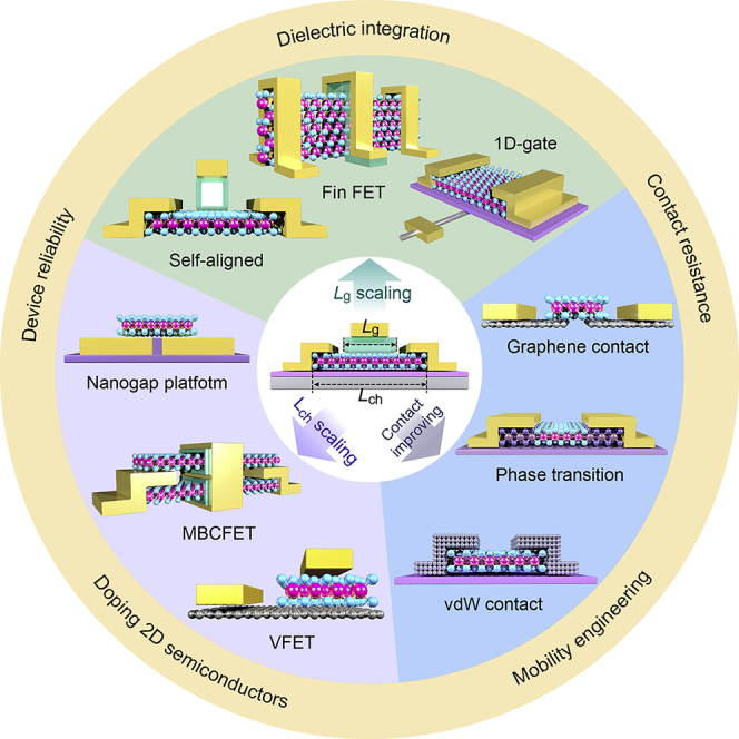
In this review, we will first discuss the fundamental intrinsic properties of 2D semiconductors such as the band gap, effective mass, carrier and heat transport, illustrating their suitability for short-channel devices. After that, we introduce state-of-the-art strategies for achieving ultra-scaled 2D transistors in the aspects of the channel, gate, and contact length, as shown in Figure 3. For the scaling of the channel length, we mainly focus on the techniques of electron beam lithography and controlled phase transition, and the device configurations based on 2D nanogap, multi-bridge channel, and vertical channel. For the scaling of the gate length, we include transistors with one-dimensional gates, self-aligned engineering, and fin-type structured field-effect-transistor (FinFET) configuration. For the scaling of contact lengths, we focus on edge-contact techniques in the aspects of both top-down and bottom-up strategies, including edge metallization, phase engineering, and heterostructure engineering. Among them, we not only present the innovative techniques and processes but also summarize the achieved parameters for performance evaluation accordingly, which could provide a comprehensive view of ultra-scaled 2D transistors. Finally, we identify key opportunities and challenges for integrating ultra-scaled 2D transistors in the post-Moore era.
Figure 3.

A summary of ultra-scaled 2D transistors achieved through shrinking the channel and gate length, respectively
Intrinsic properties of 2D semiconductors for transistors
Although the majority of the scientific community remains optimistic about the prospective of 2D materials in next-generation electronics, it is argued that not all 2D materials are equally suitable for constructing FET channels (Khan et al., 2020). A set of intrinsic properties of 2D semiconductors should be taken into account to evaluate their suitability for high-performance transistors. The most intuitive example is the pristine graphene possessing gapless nature, which has been validated to be fundamentally inconsistent with the requirement for proper operation of semiconducting FETs (Schwierz, 2013). Indeed, a variety of material properties such as bandgap, carrier effective mass, heat transport, and contact resistance, should be considered in a collective and complementary mode to realistically evaluate the suitability of this material family for transistors. In this section, we discuss the applicability of 2D materials in post-Moore FETs, on the basis of their relevant parameters and properties.
Bandgap (EG) has been identified as a crucial factor influencing the performance of 2D materials-based devices, owing to its decisive effect on the off-state current and on/off ratio of transistors, where m is a factor of 2 or larger depending on the transistor configuration, kB is the Boltzmann constant, and T is the temperature (Kim et al., 2011). For example, to ensure the functionality of a logic FET, the bandgap of channel material is required to be at least 400 meV for a sufficiently high on/off ratio and effective switch-off (Kim et al., 2011; Reddy et al., 2011; Schwierz, 2010). As we stated above, the natural graphene sheet behaves as a Dirac semimetal with inherently zero bandgap, which is thus unsuitable to be used as the FET channel materials. Semiconducting TMDs such as MoS2 and WSe2, exhibit intrinsic bandgap ranging from 0.5 to 2.0 eV which is comparable to that of Si (Chaves et al., 2020; Choi et al., 2017; Duan et al., 2015). Moreover, the bandgap of TMDs generally undergoes an indirect-to-direct transition as being thinned down from thicker crystal to monolayer form, offering more flexibility in the demand-driving device design and architecture (Kang et al., 2017b; Lezama et al., 2015; Zhang et al., 2014). Therefore, we could conclude that the semiconducting TMDs possess advantages in satisfying the fundamental criteria for FET channels from the bandgap aspect.
Another significant factor is the charge transport property of the channel materials, where fast response of the charge carriers to the change in external electric field is highly demanded. Device parameters, mainly including the mobility, peak velocity, and saturation velocity, provide direct measurements of the efficiency of such field response (Cheng et al., 2014; Seo et al., 2016). Among them, high mobility is the most straightforward indicator for a fast-response FET. In the linear regime, the mobility is inversely proportional to the carrier effective mass, suggesting that the lower effective mass is beneficial for achieving higher mobility (Chhowalla et al., 2016). However, as continuously down-scaling the channel length, unfavorable source-to-drain tunneling current starts to emerge in the transistors with extraordinarily high mobility, leading to the performance degradation owing to the weakened electrostatic control on the channel (Cheng et al., 2019; Luo et al., 2021). Moreover, the small effective mass results in a low density of states (DOS), which requires a much larger gate voltage to achieve high on-current, thus causing the degradation of the switching characteristic in the device (Klinkert et al., 2020; Schenk et al., 2020). To resolve this issue, the channel material is expected to possess optimal carrier effective mass to avoid the tunneling current arising from the sizing effect, while maintaining sufficiently high DOS. Previous reports have investigated the tunneling behavior of TMD FETs with 5 nm source-drain distance, where Mo-based TMDs were identified to be more appealing than the W-based counterparts, owing to their optimal effective masses together with sufficiently high mobility (Bernardi et al., 2017; Nichols et al., 2016; Pang et al., 2020).
In addition, the Joule heating in a FET channel originating from the current flow is also a determining factor of the device performance, in which the heat must be effectively released to avoid over-heating-induced degradation. In a standard FET with three-terminal planar structure, efficient heat dissipation requires high thermal conductivity of both the channel and substrate, as well as low thermal boundary resistance at each interface. The thermal conductivity of TMDs is not obviously advanced comparing with Si-based bulk materials as stated in previous reports, thus exploring high-quality dielectric materials with high thermal conductivity and atomically clean interface might be the mainstream for developing TMD-based high-performance FETs (Bae et al., 2019; Liu et al., 2019a; Wang et al., 2014). Won Jong Yoo’s group reports that self-heating is impeded along the black phosphorus (BP) and dielectric interface, which leads to a thermal plateau inside the channel and eventual Joule breakdown (Ali et al., 2019). Additionally, the authors extracted the thermal conductance to be 1-10 mW m−2·K−1 at the BP-dielectric interface by using a size-dependent electro-thermal transport model. Two different dielectric materials including hexagonal boron nitride (h-BN) and SiO2 are used in the BP devices, in which much higher breakdown power density and electric field endurance together with efficient and homogeneous thermal spreading are observed in the h-BN supported device, owing to its more superior structural and thermal compatibility with BP. This work illustrates that h-BN is more advantageous for efficient cooling in BP devices than that of SiO2 substrate. To further mitigate the early breakdown and uneven thermal spreading in BP devices, the same group fabricated the devices in the vertical vdW structure. The vertical device possesses 230 times higher field strength and one order enhancement in power sustainability compared with those lateral devices, owing to the integration of thermally favorable constituent materials and the formation of the optimal path for self-heat removal in the vertical configuration (Ahmed et al., 2017). Saptarshi Das’s group investigated the current distribution among the individual layers in multilayer 2D systems (Das and Appenzeller, 2013). They found that the “Hot-Spot”, which is the centroid of the current distribution, migrates dynamically within the interlayers, resulting in an unusual trend in the effective contact resistance which is mainly determined by the effective interlayer resistance. This work reveals the fundamental information about the charge transport in 2D systems, which may play a crucial role in the implementation of future electronics.
Apart from the above-mentioned intrinsic properties, a semi-extrinsic parameter, the contact resistance, is revealed to be of equal importance for 2D transistors. The ion implantation technique has been widely used to highly dope the contact areas in Si transistors, which is beneficial to realize ultra-low contact resistance below 50 Ω μm (Taylor et al., 2013; Wong et al., 2017). In contrast, direct deposition of bulk metal contacts onto the 2D plane generally introduces gap states that lead to the Fermi level pining (FLP) effect, usually leading to a large contact resistance in the magnitude of several kΩ·μm using TMDs as channel materials (Durán Retamal et al., 2018; Liu et al., 2022). For this reason, various approaches have been developed to eliminate the FLP effect for low Schottky barrier height and contact resistance, such as the transfer of vdW bonded bulk metal, metallic or semi-metallic 2D materials-based electrodes, as well as the phase engineered seamless contacts (Huang et al., 2020a; Schulman et al., 2018). All these strategies address the contact issue to some certain extent, making semiconducting TMDs viable candidates for FETs with proper functionalities. During the submission of this article, we become aware of a review about the structural properties, doping, contact engineering of 2D semiconductors (mainly TMDs), which also provided detailed discussions on the advanced devices beyond CMOS technology (Shen et al., 2022). These contents are equally important for the ultimate device scaling and performance optimization, and we refer to interested readers to this review.
Channel length scaling of transistors
The atomically thin feature of 2D semiconductors gives rise to the promise of ultra-scaled transistors beyond the physical limit of Si-based electronics, which inspires intensive research in the design and fabrication of 2D short-channel devices (Chhowalla et al., 2016; Liu et al., 2021c). In this section, we will demonstrate some representative 2D short-channel devices categorized by device configurations and fabrication techniques. The discussion follows a progressive manner in the consideration of the channel length, as well as the innovativeness of the corresponding device fabrication scheme, aiming to provide a comprehensive overview of ultra-scaled 2D transistors achieved by channel length scaling.
Ultrafine electron beam lithography
Electron beam lithography (EBL), a widely incorporated technique in nano-device processing, shows great potential in the direct patterning of short-channel 2D transistors for practical applications (Gao et al., 2018; Jiang et al., 2022; Li et al., 2020b), in which huge progress has been achieved. For instance, Jing Kong’s groups (Shen et al., 2021) report monolayer MoS2 FETs with a channel length of 35 nm utilizing semimetal (Bi) as contacts (Figure 4A), in which a considerably low contact resistance (Rc) of 123 Ω μm with negligible Schottky barrier height is achieved, owing to the saturation of the metal-induced gap sates (Figure 4B). The ultra-low contact resistance promises a record high on-state current density (Ion) of 1135 μA μm−1 and high carrier saturation velocity (vsat) of 2.5 × 106 cm s−1 at low Vds = 1.5 V (Figure 4C), delivering comparable performance to modern silicon transistors with similar dimensions (Figure 4D). It is envisioned that the Ion could be further improved to 1800 μA μm−1 in a 10-nm-channel monolayer TMD FET at a n2D of 4.5×1013 cm−2 in a foreseeable future, which meets the industrial goal of next-generation transistor technologies. This work suggests the feasibility of fabricating 2D short-channel devices by employing the simple lithography processes while ensuring robust device performance via semimetal contacts. Xinran Wang’s group fabricated MoS2 transistors with an even shorter channel length of 20 nm using the same EBL technique (Li et al., 2019). Through employing the monolayer molecular crystal of 3,4,9,10-perylene-tetracarboxylic dianhydride (PTCDA) as a buffer layer, the HfO2 dielectric with an equivalent oxide thickness (EOT) of 1 nm was successfully integrated with the MoS2 device (Figure 4E). The breakdown field (Ebd) reaches up to 16.5 mV cm−1, and the leakage current can be as low as ∼10−2 A·cm−2 at the 1 nm EOT, satisfying the International Technology Roadmap for Semiconductors (ITRS) low-power requirements for CMOS. Thanks to the outstanding characteristics of the PTCDA/HfO2 gate dielectric, the short-channel MoS2 transistors exhibit a high carrier mobility of 34 cm2 V−1·s−1, current on/off ratio over 107, and subthreshold swing (SS) down to 73 mV· dec−1 (Figure 4F).
Figure 4.

Channel length scaling of 2D transistors based on EBL technology
(A) Schematic of monolayer MoS2 transistor using semimetal Bicontacts.
(B) Band alignment between semimetal and semiconductor. The metal-induced gap sates (MIGS) in semiconductor are saturated when contacting with semimetal, leading to the negligible Schottky barrier height as well as low contact resistance.
(C) Output curves of short channel MoS2 transistor measuring at different gates from −10 V to 30 V. The maximum Ion can be as high as 1135 μA μm−1; Inset shows the SEM image of the as-fabricated device.
(D) Projected ION as a function channel length for monolayer TMDs transistors using different contact technologies. Figures A, B, C, and D are reproduced with permission from (Shen et al., 2021) Copyright© 2021, Springer Nature.
(E) Schematic illustration of the hybrid ML PTCDA/HfO2 gate stack on 2D materials. Inset: a 10 nm × 10 nm high-resolution STM scan of ML PTCDA on graphene.
(F) Transfer characteristics of the short channel ML MoS2 transistor using ultrathin PTCDA/HfO2 gate dielectric. Inset shows the corresponding SEM image of the transistor. Figures E and F are reproduced with permission from (Li et al., 2019) Copyright© 2019, Springer Nature.
(G) Schematic of the two-step EBL fabrication process for achieving the 2D short channel transistors in sub-20 nm.
(H) Transfer characteristics of the ML MoS2 transistor fabricated by the two-step EBL process; Inset shows the SEM image of the transistor with a channel length of 14 nm.
(I) Current on/off ratio as a function of VDS with a channel length of 14 and 50 nm, respectively. Figures G, H, and I are reproduced with permission from (Zhu et al., 2018) Copyright© 2018, American Chemical Society.
It is important to note that the real resolution e.g. feature size and half-pitch of EBL is quantified by the point spread function, which determines the nanoscale energy deposition into the resist (Manfrinato et al., 2014). The overlap of such spread energy profile gives rise to the limitations in the practical pattern density obtained by the single-step EBL approach, making it difficult to further downscale the channel length approaching 10 nm (Manfrinato et al., 2013). On the other hand, decreasing pitch size generally introduces additional challenges in the electrodes lift-off process, which might deteriorate the device performance owing to the rougher edges of the metal contacts (Peng et al., 2014; Tinoco et al., 2017).
By adopting a two-step EBL process, James C. Hone’s group (Zhu et al., 2018) successfully fabricated monolayer MoS2 FETs with a channel length of 14 nm on thin layer HfO2 dielectric. The source electrodes with a pitch size of 400 nm were firstly patterned and metallized, followed by the deposition of drain electrodes (width >350 nm) between each pair of source contacts via a second EBL cycle (Figure 4G). The as-fabricated transistors exhibit a high current on/off ratio of 3.3 × 10⁶ and a low SS of 86.5 mV·dec−1 at Vds = 0.1 V (Figure 4H). Although the on/off ratio progressively decreases with increasing the bias voltage, it remains over 105 when Vds is below 2 V, suggesting the effective immunity to the short-channel effects of the devices (Figure 4I).
While the two-step EBL approach is promising to achieve ultra-scaled 2D transistors, it suffers from the difficulties of precisely positioning the drain electrodes in the middle of the source pairs, leading to the low success rate in device fabrication and the significant variations in the channel length, especially when attempting to further reduce the channel size. Nevertheless, ultrafine EBL is still one of the most powerful tools in processing the ultra-scaled 2D transistors, where intensive engineering in the exposure system might be a potential route toward the realization of sub-10 nm channel length (Manfrinato et al., 2013).
Nanogap
As discussed in the previous section, it is extremely difficult to realize ultra-short channel length without compromising the device yield and performance uniformity in the sub-10 nm regime by solely relying on state-of-the-art EBL-related techniques (Jing et al., 2020). In this context, more innovative methods are to be developed to further reduce the channel dimension with improved precision and controllability. In recent years, 1D structures such as single-walled carbon nanotubes (SWCNTs) and nanowires with ultra-small diameter have been utilized as masks for contact deposition instead of using EBL-patterned resist layers (Bao et al., 2018). In this case, the channel length of transistors is determined by the diameter of these 1D structures, making it possible to access the sub-10 nm regime. For example, Qunqing Li’s group reported that horizontally aligned SWCNTs could be suspended above substrates via being clamped by a resist double layer, which serves as masks in the metal deposition process (Xiao et al., 2019). Briefly, the first layer of ZEP-520A resist (mixture of 11% methyl styrene and chloromethyl acrylate copolymer and 89% anisole) was spin-coated onto the substrate, upon which the SWCNTs supported by polymethyl methacrylate (PMMA) was transferred to form a sandwich structure. EBL-defined window was then developed to obtain the suspended SWCNT masks, yielding a series of nanogaps with ∼7.5 nm in size that defines the channel of transistors after electrode metallization (Figure 5A). This technique enables the fabrication of parallel 2D short-channel transistors with high successful rate and moderate electrical transport performance, e.g. mobility of 17.4 cm2 V−1·s−1, SS of 120 mV·dec−1, and on/off ratio of ∼107. Such CNT mask strategy could be further improved by developing guided/self-aligned CNT growth methods to achieve ultra-clean SWCNT arrays with more controllable bundle density and very high degree of alignment (angle SD of ∼0.03°), which are essential to achieve large-scale fabrication of short-channel devices with superior performance and excellent uniformity (Guo et al., 2022; Hong et al., 2010).
Figure 5.

Channel length scaling of 2D transistors with nanogap
(A) Upper: schematic diagram of nanogaps achieved by suspended SWCNT masks; Below: SEM image of the corresponding nanogaps in 7.5 nm. Reproduced with permission from (Xiao et al., 2019) Copyright© 2019, American Chemical Society.
(B) Upper: Schematic diagram of nanogaps on Bi2O3 substrate via HNO3 etching. Below: the as-fabricated short channel MoS2 transistor in top-gate configuration.
(C) Transfer characteristics of the MoS2 transistor with channel length of 8.2 nm.
(D) Output characteristics of the inverter based on 2D short-channel transistors. Figures B, C, and D are reproduced with permission from (Xu et al., 2017) Copyright© 2017, American Chemical Society.
(E) Schematic image of the short-channel device fabricated by transferring 2D flakes on top of utraflat template-stripped metal electrodes with nanoscale gap.
(F) AFM image of MoS2 flake on Au surface with a nanogap. Figures E and F are reproduced with permission from (Namgung et al., 2021) Copyright© 2021, American Chemical Society.
(G) Schematic illustration of graphene-contacted ultra-short channel MoS2 transistors in top-gated geometry.
(H) Transfer characteristics of the 4 nm top-gated MoS2 transistors at different bias voltages from 20 to 100 mV. Inset shows the corresponding AFM image.
(I) Channel length-dependent current on/off ratio, mobilities, SS, and DIBL of back-gated MoS2 transistors. Figure G, H, I are reproduced with permission from (Xie et al., 2017) Copyright© 2017 WILEY-VCH Verlag GmbH & Co. KGaA, Weinheim.
In comparison to the CNT mask technique, building the dielectric nanogap platform onto which the 2D materials are transferred could be a more holistic and scalable alternative to achieve short-channel devices (Chen et al., 2021). Jun He’s group reported a novel and universal method to fabricate large-scale nanogaps deriving from a corrosion crack along the cleavage plane of β-Bi2O3 (Xu et al., 2017). As shown in Figure 5B, the nanogap was formed by consecutive deposition of the HfO2 dielectric and Au electrodes onto the HNO3 etched β-Bi2O3 layer. Subsequently, monolayer MoS2 was transferred on top of the electrodes, where an additional layer of HfO2 was deposited by ALD, serving as the gate dielectric. The resultant MoS2 transistor possesses a channel length of 8.2 nm defined by the width of the nanogap, exhibiting promising electrical transport performance including low SS of 140-170 mV·dec−1, high current density of ∼2.5 μA μm−1, and high current on/off ratio of 106-107, as shown in Figure 5C. The logic inverter based on the short-channel transistors is also demonstrated in this work. The high and low Vout corresponding to logic 1 and 0 can be clearly observed in the output curves when gradually increasing the Vin, suggesting the potential of scaling 2D logic devices to the sub-10 nm regime (Figure 5D).
Sang-Hyun Oh’s group (Namgung et al., 2021) also created the ultra-narrow nanogap through partial etching and re-coating of Al2O3 layers at pre-defined thicknesses, together with the deposition of metal electrodes. The whole structure was then mechanically peeled off and flipped to reveal the ultra-flat surfaces consisting of lateral Au-Al2O3-Au structure. 2D flakes could be simply transferred on top of the platform, where the Al2O3 nanogap effectively defines the conducting channel with ultra-short length of ∼10 nm (Figure 5E). The AFM image shown in Figure 5F illustrates the clean and smooth surface of the MoS2 flake and the metal electrodes. It is worth noting that the root-mean-square roughness of the vertically aligned source/drain electrodes can be as low as 0.315 nm by carefully controlling the ALD deposition and chemical etching of the Al2O3 dielectric layer, which is essential to enhance the device performance owing to the minimized charge scattering and reduced contact resistance correspondingly (Zheng et al., 2021).
It is noted that the main processing techniques of fabricating the above nanogap-based transistors are wafer-scale compatible, making it possible to achieve the ultra-scaled 2D transistors in arrays for more advanced applications (Jeong et al., 2022). Additionally, the nanogap approach could effectively avoid the surface damage of 2D channels caused by the direct electrode deposition that is commonly observed in the EBL-related procedures even for the CNT mask method, which might degrade the device performance (Radisavljevic et al., 2011). On the other hand, it is worth noting that the minimum size of the nanogap and the corresponding device performance are strongly correlated with the thickness and quality of the ALD-coated dielectric layers. Therefore, it is essential to optimize the growth condition of the dielectric layers, which may achieve the narrower gap, and promote significant advances in nanogap-based high-performance short-channel transistors (Illarionov et al., 2019; Li et al., 2019).
Besides the above-mentioned nano-processing techniques, the intrinsic feature of 2D materials could offer additional opportunities for the realization of ultra-short channels. Guangyu Zhang’ group (Xie et al., 2017) reported a graphene-based grain boundary widening technique to fabricate the 2D short-channel FETs. In this work, the 1D grain boundary in monolayer graphene is selectively etched by using hydrogen plasma, resulting in a nanogap with well-defined width. The channel material is then transferred onto the nanogap, where the remaining graphene sheets serve as the source-drain electrodes (Figure 5G). As shown in Figures 5H and 5I, the monolayer graphene-contacted MoS2 FETs with channel length scaling down to ∼4 nm exhibit promising electrical transport performance including a current on/off ratio of ∼2.6 × 10⁶, off current density of ∼5 pA μm−1, SS of ∼208 mV·dec−1, and DIBL of ∼1.03 V V−1. This work provides a facile route toward the fabrication of various 2D materials-based devices with nearly Ohmic contacts for ultra-scaled electronics. Recently, Wei Lu et al. reported the fabrication of nanogaps using tilted-angle disposition method. In this work, a two-step deposition approach was utilized to achieve BP-based short-channel devices. In the first step, 4 μm channel was defined using UV lithography, followed by the electrode metallization. Secondly, another lithography process was performed, after which the electrode deposition was conducted along a tilted angle θ instead of the perpendicular direction. The resultant channel lengths ranging from 100 nm to 20 nm can be effectively controlled by adjusting the tilted angle from 65° to 40°. This approach is favourable for improving the sensitivity and response speed of terahertz photodetectors by exploring the photo-thermoelectric effect in an ultra-short 2D channel (Guo et al., 2020).
Vertical channel
In contrast to the general 2D transistors where the planar electrical transport is still preserved, ultra-short vertical conducting channels can be realized by taking advantage of the atomically thin nature of 2D materials. Ideally, the channel length of such vertical transistors is determined by the thickness of 2D flakes, which can be easily down-scaled to the sub-nanometer regime by adopting their monolayer form. Moreover, devices in vertical configuration could offer more flexible integration schemes compared to the strict planar structure (Su et al., 2021; Wang et al., 2021; Zhang et al., 2021).
Recently, Young Hee Lee’s group reported 2D vertical FETs by transferring MoS2 onto the prefabricated source-insulating spacer-drain patterns, in which either the Al2O3 film or h-BN was utilized as the spacer and top-gate dielectric (Jiang et al., 2020). Figure 6A schematically illustrates the vertical FET structure, in which the effective channel length is defined by the thickness of the Al2O3/h-BN spacer (∼10 nm, inset of Figure 6B). The device exhibits excellent electrical transport performance including large on-current density of 70 μA μm−1 and high on/off ratio ranging from 107 to 109 by using the chemical vapor deposition (CVD) grown monolayer MoS2 sample. Figure 6B compares the transport performance of the MoS2 transistors in both vertical and lateral configurations, where the Ion is greatly improved by two orders of magnitude for the vertical device with maintained on/off ratio, suggesting its advantages over the conventional planar structure (Liu et al., 2018b; Wang et al., 2019). Such vertical configuration is also applicable to other 2D semiconductors with similar performance enhancement, which is verified by the MoTe2 transistor in ambipolar transport characteristic.
Figure 6.

Channel length scaling based on vertical device configuration
(A) Schematic illustration of the 2D vertical FET with mainly six layers which are the bottom electrode, insulating spacer, top electrode, 2D vertical channel, top-side gate insulator, and gate electrode.
(B) Transfer characteristics of the 2D vertical FET and conventional 2D planar FET. Inset: schematic illustration of the local enhancement of electric field in 2D vertical FET. Figures A and B are reproduced with permission from (Jiang et al., 2020) Copyright© 2020 WILEY-VCH Verlag GmbH & Co. KGaA, Weinheim.
(C) Cross-sectional schematic of 2D vertical FET fabricated by using vdW electrodes. The items from bottom to top are graphene, MoS2, and vdW electrode, respectively.
(D) 2D plot of Ids versus temperature (y axis) and gate voltage (x axis) for the device with vdW electrode. The bias voltage is fixed at 0.5 mV. Figures C and D are reproduced with permission from (Liu et al., 2021b) Copyright© 2021, Springer Nature.
(E) Schematic diagram of the 2D vertical FET based on SWCNT network and MoS2 heterostructure.
(F) Electrostatic screening effect simulation of the gate electric field in the SWCNT network/MoS2 heterostructure. The red arrows indicate the electric field from the Si gate through the SWCNT electrode, MoS2 channel, to the Au metal electrode. Figures E and F are reproduced with permission from (Phan et al., 2019) Copyright© 2019, American Chemical Society.
Apart from defining the conductive channel using insulating 2D spacers, sandwiching the semiconducting TMDs between bulk metal and graphene electrodes also enables the realization of a vertical transistor, in which the thickness of the semiconductors directly determines the channel length. By incorporating the method of transferring vdW metal electrodes, Yuan Liu’s group (Liu et al., 2021b) reported that the vertical transistor with channel length down to the monolayer scale can be readily achieved (Figure 6C). Arising from the minimized direct tunneling current and FLP effect, the vertical FETs exhibit on-off ratios of 26 and 103 for channel lengths of 0.65 and 3.60 nm, respectively. The temperature-dependent measurements illustrate that the on/off ratio of the 3.0 nm channel length device is around 758 at room temperature, which is greatly improved to ∼105 at 77 K (Figure 6D). This behavior indicates that the thermionic emission mechanism governs carrier transport in the vertical device with the optimized metal contacts using vdW integration, in great contrast to the tunneling leakage current dominated traditional devices under direct metal deposition (Zhang et al., 2021). Jonghwa Eom’s group demonstrated a vertical FET in a similar structure, in which multilayer MoS2 was used as the channel material. The corresponding device exhibits a large current density of 105 A·cm−2 and a high current on/off ratio of ∼106 (Farooq Khan et al., 2017).
It is noted that the semi-metallic nature of graphene could significantly weaken the back-gate electrostatic control on the TMD channel owing to the screening effect, leading to the degradations in both the on-state current density and on/off ratio. Woo Jong Yu and coworkers (Phan et al., 2019) reported that the SWCNT network can be used as the bottom electrode instead of graphene (Figure 6E), which enables effective transport of the gate field through the empty space of the network, thus providing direct modulations on the band alignment at the channel/CNT interface (Figure 6F). As a result, more than 10-fold increase in the on/off ratio can be achieved in the CNT-based vertical FET compared to the devices with graphene contact.
Multi-bridge channel
In the trend of continuous development of the technological node, conventional three-terminal transistors in planar configuration encounter severe problems in further improving the device performance owing to the restricted gate controlling capability, which arises from the quantum confinement effect. Multi-bridge channel field-effect-transistor (MBCFET), formed by vertically stacking the conductive channels in a gate-all-around (Pizzocchero et al., 2016) configuration, has been identified as a very promising candidate to achieve ultimate transistor scaling owing to its outstanding electrostatic controllability and power/area efficiency (Tang et al., 2020).
MBC structures based on 2D semiconductors have been experimentally realized, demonstrating robust device performance. Peng Zhou’s group reported for the first time a 2-level-stacked MoS2 ultrathin MBCFET with a channel thickness of 1.2nm/0.6nm, in which h-BN and graphene were utilized as the dielectric layer and electrodes to construct the GAA geometry (Huang et al., 2020b). The high-resolution TEM image and the corresponding EDS mapping illustrate the clean interface of the heterostructures without any contamination, which is important to ensure the high-efficient carrier transport and good gate controllability of the device. This ultrathin MBCFET exhibits a high drive current of 13.2 μA μm·μm−1 at Vds = 1V, and a minimum SS of 60 mV·dec−1 at room temperature. Notably, the leakage current of the device is as low as 0.92 pA μm·μm−1, which is only 6.5% of that in the Si MBCFET, illustrating its superiority in the aspect of low-power-consumption electronics compared to the Si-based devices (Barraud et al., 2020). The same group further investigated the MoS2 MBCFET fabricated through vdW assembly (Figures 7A and 7B), where excellent current-controlling ability and high on/off ratio of 4×10⁸ are observed (Huang et al., 2021a). More intriguingly, the normalized drive current in each level channel of the device is 23.11 μA μm·μm−1, exceeding that of the latest seven-level-stacked Si MBCFET, while the leakage current is only 0.4% of this value (Barraud et al., 2020), further suggesting its great potential in the applications of high-performance and low-power-consumption electronics (Figure 7C).
Figure 7.

2D MBCFETs
(A) Schematic structure of MBCFET with two-level-stacked channels.
(B) High-resolution TEM and EDS mapping of the MBC FET.
(C) On-state and off-state current of 2D ultrathin MBCFET dependent on the VD voltage bias. Figures A, B, and C are reproduced with permission from (Huang et al., 2021a) Copyright© 2021 WILEY-VCH Verlag GmbH & Co. KGaA, Weinheim.
(D) Structure schematic of the 2-stacked MoS2 nanosheets device. The ALD-grown HfO2 is used as the dielectric layer in the device.
(E) Transfer characteristics of the short channel MoS2 MBC FET with Lch of 160 nm. Inset shows the corresponding SEM image displaying the Lg and Lch. Figures D and E are reproduced with permission from (Xiong et al., 2021) Copyright© 2021, IEEE.
(F) One-step 2D-channel formation on suspended bridges. Reproduced with permission from (Liu et al., 2021a) Copyright© 2021 WILEY-VCH Verlag GmbH & Co. KGaA, Weinheim.
To improve the scalability of 2D MBCFET and facilitate its functionalities in heterogeneous circuitry, large-scale TMD monolayers synthesized by the CVD technique have been utilized in the GAA structure instead of the mechanically exfoliated flakes. Yanqing Wu’s group (Xiong et al., 2021) demonstrated a short-channel MoS2 MBCFET consisting of two CVD grown monolayers as conductive channels, which are stacked by sequentially layer-by-layer fabrication process (Figure 7D). The ultimate scales of the channel and gate lengths in the resultant devices are approximately 160 and 100 nm, respectively. The device exhibits robust electrical transport performance including low SS of 126 mV·dec−1, high on/off ratio of ∼107, and large on-state current density of 420 μA μm−1 at Vds = 1 V (Figure 7E). Moreover, it is worth mentioning that this work provides the first demonstration of vertically stacked 2D complementary FETs which exhibits excellent logic inverter function with a moderate gain around 10 V/V at Vin = 1.5 V. It is noted that the MBCFET configuration could promise 50% footprint reduction compared to the planar transistor structure for logic devices. In addition to the complementary logic devices, the advantages of implementing 2D MBCFETs in static random-access memory (SRAM) have also been investigated (Liu et al., 2021a). The simulation results show that the read access time and write time of 2D SRAM in MBCFET configuration can be largely reduced by 41 and 38%, respectively, in comparison to the corresponding Si nanosheet FETs (NSFETs).
These conceptually demonstrated 2D MBCFETs, albeit promising candidates with superior electrostatic controllability for applications in low-power-consumption electronics are still a fair way off from being integrated in large-scale functional circuits, owing to the complicated device structure and the difficulties in process integration. Although Zhou et al. experimentally displayed the 2D MBCFET as a proof-of-concept, the mechanical exfoliation of 2D flakes followed by the layer-by-layer stacking process is time-consuming and cost-ineffective. Additionally, CVD-grown 2D semiconductors on large scale have been utilized by Wu et al. to fabricate the MBCFETs in arrays, the tradeoff between the synthetic temperature of the 2D materials at upper tiers and the critical temperature of defect formation at lower tiers should be taken in consideration. On the other hand, Intel proposed a one-step 2D channel formation method, which exhibits great potential for large-scale and low-cost manufacturing (Chau, 2019). The method begins with the construction of multiple suspended bridges, followed by the ALD deposition of transition metal and post-chalcogenization process, enabling the production of 2D channels on all of the insulating bridges at once (Figure 7F). Similarly, the thermal budget of synthesizing the 2D materials should be carefully examined. Moreover, transition metal deposition combined with post-chalcogenization generally produces 2D films with small grain size and poor quality, which should be further optimized for high-performance device applications.
Gate length scaling of transistors
With reference to the fundamental structure of a 2D transistor, scaling the effective gate length is identified as another feasible approach to achieve ultra-scaled devices in addition to engineering the channel length (Liu et al., 2012; Liu et al., 2018a). In the following, we discuss recent advances in gate length scaling techniques, which are organized as three parallel sections based on the ultimate device structures. The relevant key parameters achieved by the resultant devices are summarized accordingly.
Transistors with one-dimensional gate
As Si-based bulk structures rapidly approaching their physical limits for the effective modulation of the conductive channel, the global-gated device configurations encounter difficulties in the aspect of continuous down-scale of 2D transistors (Chhowalla et al., 2016). Recently, highly conductive 1D structures such as metallic CNTs have attracted tremendous attention owing to their typical geometrical properties, which could be implemented as local gate electrodes with nanoscale effective length to realize ultra-scaled 2D transistors (Liu et al., 2016b).
For instance, Ali Javey’s group (Nourbakhsh et al., 2016) reported the fabrication of SWCNT gated MoS2 transistors using ZrO2 as dielectric, which successfully realizes an extremely short physical gate length of 1 nm (Figure 8A). Figure 8B shows the electrical transport properties of the device under different bias voltages with ultra-low leakage floor, indicating the ability of the ∼1 nm SWCNT gate to completely deplete the MoS2 channel and thus turn off the device. The authors observed excellent room temperature switching characteristics including near-ideal SS of 65 mV·dec−1 and high on/off ratio of ∼106 (Figure 8B). The SS of the device can be further improved by simultaneously applying the CNT local gate and Si global gate, which leads to the complementary reduction in the series/contact resistance. The detailed simulation based on Sentaurus TCAD was also performed to further understand the electrostatics of the nanotube-gated 2D transistor (Figure 8C). The contour plots in the Off and On states clearly illustrate the low and high electric field in the MoS2 near the SWCNT, indicating the depleted and strong inversion channel. The effective channel length (LEFF) is defined to reveal the region of channel controlled by the SWCNT gate, which is nearly 3.9 and 1.0 nm for the Off and On states, respectively.
Figure 8.

Gate length scaling through integrating one-dimensional CNT/nanowire
(A) Cross-sectional TEM image of the bilayer MoS2 transistor with 1-nm gate length, where SWCNT and ZrO2 are used as the gate electrode and dielectric layer, respectively.
(B) Transfer characteristics and the corresponding leakage current of the SWCNT gated MoS2 transistor at VDS = 50 mV and 1 V.
(C) Electric field contour plots for a simulated bilayer MoS2 device in the Off and On states. Figures A, B, and C are reproduced with permission from (Desai et al., 2016) Copyright© 2016, American Association for the Advancement of Science.
(D) Cross-sectional TEM image of monolayer MoS2 FET gated by 1D metallic Co2Si nanowire.
(E) The relationship between channel length Lch and Co2Si nanowire radius r for MoS2 transistors in ultra-scaled gate length. Inset shows a simplified circular-shaped Co2Si nanowire. Figures D and E are reproduced with permission from (Cao et al., 2016) Copyright© 2016, IEEE.
(F) Schematic of monolayer MoS2 in side-wall gate configuration by using monolayer graphene edge gate with a thickness of 0.34 nm.
(G) Optical image of the 0.34 nm Lg side-wall transistor arrays on a 2-inch wafer.
(H) The timescale evolution of gate length in ultra-scaled 2D transistors. Figures F, G, and H are reproduced with permission from (Ren et al., 2020) Copyright© 2020, Springer Nature.
It is worth mentioning that the realization of the short-gate transistors relies on the natural geometry of CNTs, which could circumvent any high-precision patterning process and therefore significantly lower the requirements on the lithography techniques (Chen et al., 2006). More importantly, the gate length defined by the diameter of CNTs is in general smaller than 5 nm, which readily crosses the theoretically inaccessible regime for traditional Si transistors, paving the way to realize electronic devices approaching the extreme scales (Quhe et al., 2021).
In addition to the CNTs, nanowires are also identified as potential building blocks for ultra-scaled local gates in 2D transistors (Colinge et al., 2010). For example, Kaustav Banerjee’s group (Cao et al., 2016) reported that the ultrathin metallic Co2Si nanowire can be integrated into the fabrication process of MoS2 FETs, which simultaneously serves as the source-drain deposition mask and the gate electrode (Figure 8D). In this case, the physical gate length of the transistor is defined by the diameter of the nanowire, which gives rise to an effective channel length in a range of 10-30 nm depending on the morphology of the contacting point between the MoS2 and Co2Si nanowire. Significant current on/off ratio over 106 is achieved in the transistor with a considerably low off-state current of ∼10 pA μm−1. It is worth noting that the channel length is highly possible to be scaled down to 6 nm using nanowire-shaped gate with a radius of 8 nm (Figure 8E), further validating the promising scalability of thin nanowire-based 2D transistors.
Besides the 1D/2D hybridized device structures discussed above, the atomically thin nature of 2D materials offers another opportunity for the reduction of gate length through reconfiguring the device geometry into an edge-to-face alignment. Tian-ling Ren’s group (Ren et al., 2020) proposed a side-wall monolayer MoS2 transistor employing the edge of monolayer graphene as the gate electrode (Figure 8F). The 0.34 nm physical gate length of the device is defined by the single-atom thickness of monolayer graphene, which represents the ultimately accessible gate scale in a 2D transistor under state-of-the-art nanoscale technologies (Figure 8H). Moreover, this work provides a wafer-scale fabrication strategy to achieve side-wall transistor arrays with a minimum in-batch variation of device parameters e.g. on/off ratio and SS (Figure 8G), which facilitates the development of ultra-scaled transistors toward multi-functional electronic circuits and reveals their enormous potential to further extent the Moore’s Law (Jia et al., 2022).
Fin-type structured field-effect-transistor
The gate coupling efficiency plays a vital role in determining the electrical switching properties in a transistor, particularly in the extreme scale. However, when the scale approaches sub-10 nm, the gate-channel contacting area in the conventional planar device is severely restricted, which causes degradations in the gate controlling efficiency with a large leakage floor, leading to a dramatic increase in heat dissipation. To enhance the gating efficiency while maintaining a small footprint of transistors, efforts have been devoted to developing new device architectures extending in the out-of-plane direction, following which a novel FinFET has been introduced (Jurczak et al., 2009).
Initially, Chenming Hu’s group (Chen et al., 2015) fabricated a 6-layer MoS2 FinFET (fin width Wfin = 4 nm) based on a back gate Si fin structure with 2 nm-thick gate oxide, followed by the deposition of a 30 nm long front gate (Figure 9A). The hydrogen plasma treatment was further employed to achieve a molybdenum-rich surface to lower the sheet resistance of the MoS2 channel. As shown in Figure 9B, the transfer characteristics of the MoS2 FinFET demonstrate a current on/off ratio over 105 and Ion of ∼200 μA μm−1 at 1 V operation bias, illustrating the great potential of the fin-structure-based TMD transistors in ultra-scaled technological node (Figure 9C). Similarly, Huaxiang Yin’s group (Pan et al., 2019) reported a Si fin structure gated monolayer MoS2 transistor on the scale of 10 nm. The device exhibits excellent switching behavior with average drain current on/off ratio exceeding ∼106, indicating high-efficient modulation of the MoS2 channel through the Si fin back gate.
Figure 9.

2D FinFETs
(A) Cross sectional TEM image of MoS2 FinFET using Si back gate.
(B) Transfer characteristics of the MoS2 FinFET with 4 nm thin body sweeping by the front gate voltage. Inset shows the SEM image of the device for measurement.
(C) The development trends of the FinFET channel thickness and gate length. Figures A, B, and C are reproduced with permission from (Chen et al., 2015) Copyright© 2015, IEEE.
(D) Left: The simulated field effect curves of 4 nm gate length FinFET. Right: Statistics of on/off ratio and mobility of MoS2 ML-FinFET.
(E) Schematic illustration of the 2D FinFET with Wfin of 0.6 nm. The monolayer MoS2 crystal is grown over a 300 nm height Si step with the side wall coated by HfO2 dielectric.
(F) A timescale evolution of Wfin for the transistors in FinFET configuration. Figures D, E, and F are reproduced with permission from (Chen et al., 2020) Copyright© 2020, Springer Nature.
More recently, by adopting a bottom-up fabrication route, Zheng Han’s group (Chen et al., 2020) demonstrated a vertically aligned monolayer MoS2 FinFET (ML-FinFET) with Wfin of ∼0.6 nm, which is realized by adapting a template-growth method (Figure 9D). Firstly, a 300 nm step edge is etched from a planar Si on the insulator wafer, followed by the coating of 10 nm HfO2 achieved via ALD and anisotropic dry etching. After that, monolayer MoS2 crystal is conformably grown on the step edge with the deposition of source-drain electrodes. The planar portion of the as-grown MoS2 is then etched via the plane-removing process. Finally, wet etching is performed to remove the silicon step followed by the metallization of the gate electrode, achieving the MoS2 FinFET with sub-1 nm Wfin. The current on/off ratio of the monolayer FinFET approaches ∼107, suggesting the robustness of the device (Figure 9E). This work pushes the Wfin of the FETs to an atomic physical limit, an order of magnitude thinner than that of state-of-the-art FinFETs, breaking the limitation of lithography precision on the Wfin, which is beneficial for lower power consumption and higher integration of next-generation nanoelectronics (Figure 9F).
Apparently, the fin-shaped structure effectively enlarges the area of gate-channel interface without compromising the miniaturization of the device footprint, which significantly strengthens the gate controllability, thereby alleviating the short channel effect occurring in the planar device with comparable scales. Moreover, the manufacturing process of 2D FinFETs is compatible with the mainstream silicon technology, paving a way to further extend the gate scaling in the post-Moore era (Trombini et al., 2019; Vashishtha and Clark, 2021).
Self-aligned engineering of transistors
Self-alignment technology has been proposed as an effective way to precisely position the gate electrode at extreme scales, while eliminating various unfavorable factors introduced from the lithography-related procedures, including residue absorption, interfacial traps, and parasitic capacitance/resistance.
As shown in the high-resolution TEM image in Figure 10A, Eric Pop et al. reported for the first time a monolayer MoS2-based self-aligned top-gate FETs (SATFETs), in which the Al2O3 gate dielectric scaling down to 10 nm is formed by self-passivated surface oxidation of the thermally deposited Al nano-block (English et al., 2016). The technique achieves a core-shell structure, which serves both as an anchor for the gate electrode and a hardmask for the deposition of source-drain contacts. The device exhibits high saturation current IDsat exceeding 400 μA μm−1, and low SS down to 80 mV·dec−1 with a gate length of 30 nm and EOT of 2.5 nm, suggesting the potential of 2D SATFETs in achieving high-performance ultra-scaled electronics. It is noted that the ballistic transport in 2D transistors might emerge at a scale below 100 nm, which is firstly investigated in this work. The ballistic transmission efficiency (Tr) of the MoS2 SATFETs is around 0.15 at T = 300-400 K in the saturation regime (Figure 10B), which gradually increases to 0.25 with an effective electron velocity (vEFF) of 9 × 105 cm s−1 at T = 80 K, arising from the suppression of the phonon scattering at low temperatures (Figure 10C). Nevertheless, the Tr and vEFF in the saturation regime are still far smaller than state-of-the-art silicon transistors in the similar scales. To further improve the Tr and vEFF in the ultra-scaled 2D transistors, it is essential to reduce the effective channel length (LEFF) and enhance the carrier mobility. The LEFF is determined by the profile of the top of barrier (ToB), which becomes sharper and thus results in lower LEFF by contact doping and improved EOT. On the other hand, the mobility in 2D transistors is strongly related to the carrier scattering, which can be boosted by reducing the densities of disorders, impurity charges, and phonons in the channel, as well as improving the dielectric interface.
Figure 10.

2D transistors achieved via self-aligned engineering technique
(A) Cross-sectional TEM image of the 2D MoS2 SATFET with Lg of 10 nm in false color.
(B) Transmission (Tr) vs VDS for the 2D SATFET under gate length of 10 nm at a temperature of 225 K. Inset shows conduction band diagram for the carrier transport cross the barrier.
(C) Tr and effective velocity (vEFF) as a function of temperature. Figures A, B, and C are reproduced with permission from (English et al., 2016) Copyright© 2016, IEEE.
(D) Optical images of the Bicontacted MoS2 SATFETs in arrays over 6 mm2. The corresponding false-colored SEM image of a single top-gated SATFET is also demonstrated at the bottom right.
(E) Benchmark of RC versus ION of the top-gated monolayer CVD MoS2 FETs.
(F) Benchmark of on/off ratio versus ION. Figures D, E, and F are reproduced with permission from (Li et al., 2021) Copyright© 2021, IEEE. (G) Schematic of the self-aligned GaN nanowire top-gated MoS2 FETs.
(H) Output characteristics of the self-aligned MoS2 transistor under different strains without applying gate voltage. Inset shows the schematics of the effects of strain on the transistor. Gradient ramp indicates the piezo-potential in GaN NW; red and blue indicate positive and negative piezo-potential, respectively. Figures G, H are reproduced with permission from (Liu et al., 2016a) Copyright© 2016, American Chemical Society.
On the basis of the above-mentioned fabrication strategy, Xinran Wang et al. (Li et al., 2021) reported a significant improvement in the performance of SATFETs with a gate length of 60 nm by using semimetal Bicontacts (Figure 10D). Arising from the immunity against the FLP effect, the device exhibits zero Schottky barrier height and ultra-low RC of 280 Ω‧μm which is nearly one order of magnitude smaller than that of the MoS2 transistors using traditional metal contacts such as Ag, Cr, and Au (Figure 10E). The optimized metal contacts contribute to the outstanding electrical transport performance of the SATFETs with a high ION of 680 μA μm−1, high current on/off ratio over 106, and a good SS of 120 mV·dec−1, which are much more superior than those of the CVD MoS2 transistors in top-gate configuration (Figure 10F). The SATFET arrays also exhibit excellent SCEs immunity and negligible DIBL effect, which are of great importance in the application of high-density integrated circuits. The combination of high-performance top-gate 2D FETs with large-area CVD MoS2 will significantly promote the development of 2D integrated circuits and heterogeneous systems.
In addition to the oxide-based SATFETs, semiconducting nanowires could offer an additional degree of freedom in designing new functional devices through band gap alignment to the TMD channel materials (Lin et al., 2001). Zhonglin Wang et al. (Liu et al., 2016a) reported high-performance self-aligned MoS2 FETs using p-type semiconducting GaN nanowires as local gates (Figure 10G). The fabrication process ensures the preservation of the intrinsic properties of MoS2 while suppressing the interfacial scattering rate, leading to excellent electrical transport characteristics such as high on/off ratio of ∼107 and small SS of 64 mV/dec. The photodetection properties of the device are also investigated, in which high photoresponsivity of 443.3 A·W−1 and fast response time of 5 ms are observed. The performance can be further improved with much higher photoresponsivity of 734.5 A·W−1 by applying strain on the device owing to the unique piezoelectric property of the GaN nanowire (Figure 10H).
Contact scaling of transistors
Besides the scaling of channel and gate lengths, contact scaling is another important aspect of device miniaturization. However, as the contact length (LC) is scaled closing to the carrier transfer length (LT) in a conduction channel, the area available for carrier injection is reduced, which dramatically increases the contact resistance owing to the current crowding (Allain et al., 2015; Cheng et al., 2019). In particular, the current crowding is more pronounced with the LC ≤ LT in the range of tens or hundreds nanometers, leading to the limitations on the contact scaling process (Cheng et al., 2019). Notably, edge contact geometries have been identified as a viable route toward the ultimate scale of electrical contacts, as the edge is independent of the physical contact length, especially for 2D channels with edges at the atomic scale (Figure 11A) (Lee et al., 2022; Wang et al., 2013). Additionally, the carrier transport at the metal-2D materials interface is dominated by the covalent bonding in edge-contact, which is distinct from the vdW gap existed in the top-contacted devices. This is essential to eliminate the metal-induced gap states that are responsible for the uncontrollable Schottky barrier and Fermi-level pinning effect in 2D transistors, which could substantially improve the field-effect mobility (Kim et al., 2017; Liu et al., 2022). Recently, Won Jong Yoo’s group comprehensively reviewed the 1D edge contacts for 2D material-based devices, in which state-of-the-art techniques for achieving the edge contacts, together with the charge transport and device applications of edge contacts are elaborately discussed (Choi et al., 2022). Here, we focus on the contact scaling in 2D transistors by using the edge-contact techniques.
Figure 11.

Contact scaling based on edge contact technique
(A) Schematic of 2D FET with traditional top contacts and edge contacts.
(B) Relationship between Id and Lc for in-situ edge contacts after aligning Vth, showing potential for sustaining performance while scaling contact length. Reproduced with permission from (Cheng et al., 2019) Copyright© 2019, American Chemical Society.
(C) The transfer curve of the monolayer MoS2 transistor with edge contacts. Inset shows the corresponding schematic of the device for measurement. Reproduced with permission from (Jain et al., 2019) Copyright© 2019, American Chemical Society.
(D) SEM image of the hetero-phase MoS2 transistor with Lch = 7.5 nm.
(E) MIT Virtual Source Compact modeling (MVS) of the transfer curve of the hetero-phase MoS2 short channel transistor. Inset shows circuit configuration consisting of a chain of six MoS2 FETs used in the MVS model. Figures D and E are reproduced with permission from (Nourbakhsh et al., 2016) Copyright© 2016, American Chemical Society.
(F) Transfer curve of CNT-gated p-type MoTe2 FET in 1T′-2H hetero-phase configuration. Inset shows the corresponding schematic of the device for measurement. Reproduced with permission from (Zhang et al., 2019a) Copyright© 2019, Springer Nature.
Aaron D. Franklin’s group reports the edge contact scaling in both mono- and multilayer MoS2 by using various metal-channel interfaces. The clean edge contacts of metal-MoS2 can provide immunity to the contact-scaling limitation, in which the electrical transport performance is independent of the contact length down to the 20 nm regime (Figure 11B) (Cheng et al., 2019). The in-situ Ar+ sputtering has been identified as a crucial step for producing an optimum metal-MoS2 contact, enabling the efficient charge transfer for realizing low Rc with a high density of current injection at the atomic site (Shen et al., 2021). This leads to an order of magnitude enhancement of electrical transport performance compared to the ex situ metal edge contacts. Similarly, Lukas Novotny’s group reports viable edge contact formation to h-BN encapsulated monolayer MoS2 in a polymer-free manner, by combining the techniques of reactive ion etching, in-situ Ar+ sputtering at a slightly tilted angle, and annealing (Jain et al., 2019). The transistor exhibits comparable electrical transport performance to the top-contact counterparts, in which a relatively high mobility up to ∼30 cm2 V−1 s−1, high on-current density >50 μA μm−1, and low SS of ∼116 mV·dec−1 are achieved (Figure 11C). The top-down approach via plasma etching and metallization is very promising to achieve the edge contact, whereas it yields limited success in 2D transistors owing to its stringent demands on the facilities such as an in-situ ion sputtering and metal deposition system. Alternatively, Lee Ji Ung’s group employed the 1D edge-contacted graphene as electrodes instead of metals in the h-BN-encapsulated WSe2 transistor via dry transfer technique, in which a tunable Schottky barrier with controllable ideality factor is realized (LaGasse et al., 2019).
On the other hand, 2D materials generally possess polymorphic lattice structures including the semiconducting 2H phase and the metallic 1T/1T′ phase, where the local phase transition can be realized through phase engineering techniques including catalytic synthesis, chemical treatment, and laser irradiation (Chen et al., 2020; Voiry et al., 2015). Taking advantage of this unique characteristic, 2D transistors with covalently bonded edge-contacts have been achieved through the construction of in-plane 2H-1T/1T′ hetero-phase junctions (Kappera et al., 2014). For example, Amirhasan Nourbakhsh and coworkers demonstrate a chain of alternatively connected 2H-1T′ MoS2 structures, where the deterministic phase transition is achieved by using the mask of self-assembled block copolymers followed by the n-butyllithium solution treatment (Nourbakhsh et al., 2016). The exposed MoS2 is transformed to the metallic 1T′ phase which automatically forms the seamless contacts to the semiconducting 2H phase, giving rise to a series of short-channel transistors with 7.5 nm half-pitch (Figure 11D). As shown in Figure 11E, the transistor chain exhibits an excellent on/off ratio over ∼107 with a low off-state current of 10 pA μm−1 and SS of ∼120 mV·dec−1. Moreover, the access resistance at the seamless 2H-1T′ interface is determined to be 75 Ω μm, indicating nearly ideal Ohmic contacts in the transistor chain, which demonstrates great potential to achieve efficient charge injection and ultra-low power dissipation. It is noted that the chemical treatment in the liquid phase could introduce hydrogen absorption on the MoS2 surface, which is favorable for the structural stabilization of the 1T′ phase as well as the high-quality 2H-1T′ interfaces.
In addition to the top-down strategy discussed above, the lateral heterophase junctions can be formed through bottom-up techniques by tuning the synthetic temperatures and pre-patterning precursors. Jiao liying’s group demonstrates a large-scale phase-contact strategy to obtain 1T′-2H MoTe2 homo-junction by tellurizing MoO3 and MoO2.0-2.5 (Zhang et al., 2019a). Additionally, the heterophase MoTe2 transistors in 4 nm gate length are achieved through integrating the CNT gate electrode and HfO2 dielectric layer. The ultra-scaled transistor exhibits robust performance including a high current on/off ratio of ∼105 and a low SS down to ∼73 mV·dec−1 (Figure 11F). The Schottky barrier height of such 1D edge contact is also dramatically reduced to be ∼20 meV, together with a robust mobility of ∼50 cm2 V−1·s−1. The heterophase edge contact strategy can also be extended to other 2D materials, such as the NbSe2/WxNb1-xSe2, MoS2/Mo2C, and PtSe2/PtTe2 heterostructures synthesized by the in-situ selenization in large area arrays (Choi et al., 2019; Kim et al., 2022; Vu et al., 2021). Overall, the bottom-up growth of the lateral heterophase structure demonstrates great potential to achieve edge-contacted 2D transistors on the wafer scale.
Conclusion and outlook
In conclusion, TMDs have been of central importance in the next-generation electronics with full functionality, owing to the primary merit of their atomically thin nature that allows ultra-scaled transistor architectures to approach the sub 10 nm regime. So far, researchers have made exciting progress in performance enhancement and size scaling of the 2D TMDs-based ultra-scaled transistors. The evolution of the channel and gate lengths with respect to the fabrication techniques and device geometries are summarized, together with the corresponding satisfactory performance parameters (Table 1). In the perspective of the device size, currently the physical gate length of sub-1 nm can even be realized by using graphene edge electrodes, indicating the ultimate scale of 2D transistors, which is far more advantageous than that of the conventional Si transistors (Wu et al., 2022). Moreover, the device performance has also been largely optimized owing to the extraordinary intrinsic properties of the 2D semiconductors. For example, 2D semiconductor-based MBCFETs achieve far lower leakage currents than that of the Si MBCFETs originating from their suitable band gap and carrier effective mass, illustrating their great potential in low-power electronics. Additionally, the high carrier mobility at extreme physical gate length arising from the dangling-bond-free surface in 2D materials could enable high carrier velocity and saturation current, which is essential for high-speed digital devices. Atomically thin 2D semiconductors also enable lower interlayer signal delays and more efficient heat dissipation, increasing integration density by more than 150% compared to conventional monolithic 3D integration (Jiang et al., 2019). Basically, it can be concluded that these 2D ultra-scaled transistors provide the possibility for their 3D integration compatible with the Si very large-scale integration (VLSI) technology (Akinwande et al., 2019).
Table 1.
Performance summary of the 2D short-channel transistors
| Lch/Lg (nm) | tc (nm) | μ (cm2·V−1·s−1) | RC (kΩ·μm) | VDS (V) |
Ion μA/μm |
Ioff pA/μm |
Vth V |
DIBL (V/V) | SS (mV/dec) | Ion/off | |
|---|---|---|---|---|---|---|---|---|---|---|---|
| Bi Contact (Shen et al., 2021) | 35 | ML | 55 | 0.123 | 1 | ∼900 | ∼5 | ∼ −50 | / | / | 108 |
| PTCDA/HfO2 Gate (Li et al., 2019) | 20 | ML | 34 | / | 0 | ∼50 | ∼6 | ∼ −1.8 | / | 60 | 107 |
| Two-step EBL (Zhu et al., 2018) | 14 | ML | 21,4 | 2.3 | 1.6 | 240 | ∼1 | ∼0.5 | / | 64 | 107 |
| SWCNT Masks (Xiao et al., 2019) | 7.5 | ML | 17.4 | 10.4 | 1 | 45 | ∼8 | ∼0.7 | 0.14 | 120 | 107 |
| β-Bi2O3 Nanogaps (Xu et al., 2017) | 8.2 | ML | 1.1 | / | 1 | 2.5 | 3 | ∼ −1.2 | / | 140 | 106 |
| Graphene Contact (Xie et al., 2017) | 4 | ML | 30 | 3.8 | 0.1 | ∼9 | 0.3 | ∼ −1.0 | 0.425 | 93 | 107 |
| MBCFET (Xiong et al., 2021) | 100 | ML | / | 0.77 | 1 | 420 | ∼40 | ∼ −1.5 | 0.25 | 126 | 107 |
| VFET with Al2O3/h-BN spacer (Jiang et al., 2020) | 12.6 | ML | / | 1.2–1.5 | 0.5 | 70 | ∼0.1 | ∼ −0.26 | / | / | 109 |
| Graphene/MoS2 VFET (Farooq Khan et al., 2017) | 38 | 38nm | / | −0.5 | ∼-500 | ∼-500 | ∼-25 | / | / | 106 | |
| SWCNT/MoS2 VFET (Phan et al., 2019) | 0.65 | ML | 21 | / | −2 | ∼30 | ∼104 | / | / | / | 103 |
| vdW Contact (Liu et al., 2021b) | 0.65 | 30nm | 3,81 | / | ∼0 | ∼40 | ∼104 | ∼-40 | / | / | 103 |
| Phase transition (Nourbakhsh et al., 2016) | 7.5 | 3ML | 25 | 0.075 | 1.0 | 230 | ∼10 | ∼ −0.7 | 0.1 | 120 | 107 |
| SWCNT/ZrO2 gate (Desai et al., 2016) | ∼1 | 2ML | / | / | 1 | ∼7 | ∼10 | ∼ −2 | 0.2 | 65 | 106 |
| CNT gate (Zhang et al., 2019a) | ∼4 | / | / | / | / | / | / | / | / | 73 | 105 |
| Co2Si/Al2O3 gate (Cao et al., 2016) | 6 | ML | / | / | 1 | ∼20 | 10 | ∼ −0.6 | / | 180 | 106 |
| Graphene/Al2O3 side-wall gate (Ren et al., 2020) | 0.34 | ML | / | / | −2 | ∼0.2 | ∼1 | ∼ −2 | 1 | 210 | 105 |
| 6ML MoS2 Si-FinFET (Chen et al., 2015) | 4 | 6ML | / | / | 1 | ∼200 | ∼103 | ∼ −0.6 | / | 143 | 105 |
| 1ML MoS2 Si-FinFET (Pan et al., 2019) | 10 | ML | / | / | 0.9 | ∼1.2 | ∼1 | −7 | 1 | 360 | 106 |
| Vertically Aligned FinFET (Chen et al., 2020) | ∼0.6 | ML | 10 | / | 1.0 | ∼5 | ∼0.5 | ∼ −0.7 | 0.005 | 300 | 107 |
| Al/Al2O3 -SATFET (English et al., 2016) | 10 | ML | 34 | 1.7 | 1 | ∼10 | / | / | 0.07 | 80 | / |
| Bi Contact Al2O3 -SATFET (Li et al., 2021) | 60 | ML | 35 | 0.28 | 0.1 | ∼250 | ∼30 | ∼ −4.0 | / | 114 | 107 |
| GaN -SATFET (Liu et al., 2016a) | 200 | ML | 20.7 | / | 1 | ∼10 | ∼1 | ∼ −1 | / | 64 | 107 |
The ultra-scaled 2D transistors, albeit very promising for the applications of heterogeneous integrated circuitry with extended Moore’s Law, still encounter challenges in the aspects of uniformity, stability, and reliability for the ultimate transition from concept genesis to industrial maturity. First, the uniform synthesis of high-quality single-crystalline 2D films at the wafer scale is essential for their integration in very-large-scale applications, where the uniformity in film thickness and transport performance are important factors to be considered. 2D thin films grown by conventional CVD methods are generally polycrystalline with high nucleation temperature in the range of 600-900°C, hindering their compatibility with the back-end-of-line temperature in CMOS technology (Choi et al., 2017; Huang et al., 2014; Kang et al., 2015). The exploration of low-temperature synthesis strategies (<400-500°C) for TMDs becomes increasingly crucial. Under this trend, low-temperature growth of single crystalline MoS2 and WS2 have been investigated and partially succeeded at 450°C and 300-450°C, respectively, illustrating the potential of 2D materials in future integrated circuits (Akinwande et al., 2019; Delabie et al., 2015; Jurca et al., 2017).
On the other hand, the topological or topographical defects, such as the grain boundaries, atomic vacancies, and strain fields, introduced during the 2D material preparation processes could ultimately affect the uniformity of the devices (Novoselov et al., 2004; Stoller et al., 2008). Under such circumstances, a physical transfer-process-based vdW integration approach has been demonstrated to alleviate these challenges (Jung et al., 2019; Liu et al., 2019b). The weak vdW force and relatively low processing temperatures ensure slight damage to the 2D crystals during the transfer process. It is noted that a highly controlled vacuum environment could be favorable for achieving ultra-clean interfaces with high uniformity in the large-scale transfer process (Kang et al., 2017a). Besides the uniformity, the stability of environment-sensitive 2D semiconductors (such as BP) must also be taken into consideration (Liu et al., 2021c). An effective method to alleviate material degradation in air is to encapsulate the conductive channels using in-situ grown protective layer or diffusion barrier, such as Al2O3 and HfO2, with compact lattice structures and robust air stability (Wood et al., 2014). On the other hand, surface modification is also identified as a viable route to improve material stability through the formation of covalent bonds at the surfaces, which has been confirmed in adatoms doped BP and other 2D materials (Feng et al., 2016).
In addition, the reliability of 2D materials at the device level is also an important aspect of their further industrial application, which is largely determined by the properties of channel-dielectric and channel-electrode interfaces, as well as the qualities of the insulator dielectric and metal electrodes. In particular, the introduction of defects and residues at the channel-dielectric interface can generate a series of reliability issues, such as 1/f noise, random telegraph noise, hysteresis, bias temperature instability, time-dependent dielectric breakdown, and hot carrier degradation (Das et al., 2021). The integration of defect-free crystalline insulator with a 2D channel to form a vdW interface could be an option to improve the reliability (Illarionov et al., 2020), where the dielectric materials including h-BN, Bi2SeO5, and CaF2 are proposed as the most promising candidates. However, new problems such as thermal budget and gating efficiency might emerge by using these novel dielectrics (Li et al., 2020b). Alternatively, introducing a buffer layer could also be an effective way to improve material adhesion for obtaining a high-quality channel-dielectric interface, which has been demonstrated in the preparation of uniform and ultrathin HfO2 dielectrics on 2D materials using molecular crystals of PTCDA as buffer layers (Li et al., 2019). Besides the dielectric layer, another concern is the channel-electrode interface which significantly influences the device performance. The deposition of energetic metal atoms could induce damage in the ultrathin 2D materials underneath, causing Fermi level pining effect and inefficient charge injection that are manifested as large contact resistances (Liu et al., 2018b). To solve this issue, the fabrication of vdW contacts has been reported, which provide atomically clean and electronically sharp interfaces with minimized interfacial states and tunable Schottky barrier height (Liu et al., 2021b). This approach is applicable to various device configurations including 2D/3D hybrid stacks; however, its feasibility at the wafer scale still requires further explorations (Jung et al., 2019; Li et al., 2020a; Liu et al., 2018b; Liu et al., 2019b; Zhang et al., 2019b). Additionally, edge-contact or semimetal contact are also promising approaches for realizing low contact resistance and contact scaling in 2D transistors (Yang et al., 2019; Zhang et al., 2019a).
Although challenges remain, 2D materials demonstrate great potential in the realization of lab-to-fab transition. As such, multi-pronged efforts, including wafer-scale synthesis of high-quality and uniform 2D thin films, improving device scalability and reliability, and implementation with silicon technology, need to be devoted to their ultimate applications with a fully standardized 2D industrial chain. We envision that, with the continuous progress of 2D research in both scientific and technological aspects, 2D semiconductor technology would become a global industry business with far-reaching influence.
Limitations of the study
The investigation of 2D transistors and integrated circuits has been lasted for nearly ten years, for the purpose of extending Moore’s Law. There have been numerous works in the aspects of 2D materials growth, device fabrication, doping techniques, contact engineering, and circuit integration. It is impossible to cover and cite all the related publications. Our review focuses on the recent advances in achieving ultra-scaled 2D transistors in the aspects of techniques and mechanisms. We introduce state-of-the-art strategies for realizing ultra-scaled 2D transistors in terms of channel length and gate length scaling, providing comprehensive evaluations of the corresponding device performance together with the possible optimization routes through the technological aspect. Our article illustrates a general direction on the realization of ultimate 2D transistors with extreme scales, which should be of interest in both the scientific and industrial communities.
Acknowledgments
This work is financially supported by the National Natural Science Foundation (NSF) of China (Grant No. 62104041), Shanghai Sailing Program (Grant No. 21YF1402600), Shanghai Rising-Star Program (Grant No. 22QA1401000), the Natural Science Foundation of Shanghai (Grant No. 22ZR1405700), and the young scientist project of MOE innovation platform.
Author contributions
Conceptualization: T.L. and D.X.; Investigation: T.W., Z.H, T.L, and D.X.; Writing–Original Draft: T.W., Z.H, D.X., and T.L; Writing–Review & Editing: T.W., Z.H, Q.X, X.Z., D.X., and T.L; Supervision: T.L. and D.X.; Funding Acquisition: T.L. and D.X.
Declaration of interests
The authors declare no competing interests.
Contributor Information
Tao Liu, Email: liu_tao@fudan.edu.cn.
Du Xiang, Email: xiang_du@fudan.edu.cn.
References
- Ahmed F., Kim Y.D., Choi M.S., Liu X., Qu D., Yang Z., Hu J., Herman I.P., Hone J., Yoo W.J. High electric field carrier transport and power dissipation in multilayer black phosphorus field effect transistor with dielectric engineering. Adv. Funct. Mater. 2017;27:1604025. doi: 10.1002/adfm.201604025. [DOI] [Google Scholar]
- Akinwande D., Huyghebaert C., Wang C.-H., Serna M.I., Goossens S., Li L.-J., Wong H.S.P., Koppens F.H.L. Graphene and two-dimensional materials for silicon technology. Nature. 2019;573:507–518. doi: 10.1038/s41586-019-1573-9. [DOI] [PubMed] [Google Scholar]
- Al-Mistarihi M.F., Rjoub A., Al-Taradeh N.R. 2013 25th ICM. IEEE; 2013. Drain induced barrier lowering (DIBL) accurate model for nanoscale Si-MOSFET transistor. [Google Scholar]
- Alharbi A., Zahl P., Shahrjerdi D. Material and device properties of superacid-treated monolayer molybdenum disulfide. Appl. Phys. Lett. 2017;110:033503. doi: 10.1063/1.4974046. [DOI] [Google Scholar]
- Ali F., Ahmed F., Yang Z., Moon I., Lee M., Hassan Y., Lee C., Yoo W.J. Energy dissipation in black phosphorus heterostructured devices. Adv. Mater. Interfaces. 2019;6:1801528. doi: 10.1002/admi.201801528. [DOI] [Google Scholar]
- Allain A., Kang J., Banerjee K., Kis A. Electrical contacts to two-dimensional semiconductors. Nat. Mater. 2015;14:1195–1205. doi: 10.1038/nmat4452. [DOI] [PubMed] [Google Scholar]
- Allain A., Kis A. Electron and hole mobilities in single-layer WSe2. ACS Nano. 2014;8:7180–7185. doi: 10.1021/nn5021538. [DOI] [PubMed] [Google Scholar]
- Auth C.P., Plummer J.D. Scaling theory for cylindrical, fully-depleted, surrounding-gate MOSFET's. IEEE Electron. Device Lett. 1997;18:74–76. doi: 10.1109/55.553049. [DOI] [Google Scholar]
- Bae S.-H., Kum H., Kong W., Kim Y., Choi C., Lee B., Lin P., Park Y., Kim J. Integration of bulk materials with two-dimensional materials for physical coupling and applications. Nat. Mater. 2019;18:550–560. doi: 10.1038/s41563-019-0335-2. [DOI] [PubMed] [Google Scholar]
- Bao X., Ou Q., Xu Z., Zhang Y., Bao Q., Zhang H. Band structure engineering in 2D materials for optoelectronic applications. Adv. Mater. Technol. 2018;3:1800072. doi: 10.1002/admt.201800072. [DOI] [Google Scholar]
- Barraud S., Previtali B., Vizioz C., Hartmann J.M., Sturm J., Lassarre J., Perrot C., Rodriguez P., Loup V., Magalhaes-Lucas A., et al. 2020 IEEE Symposium on VLSI Technology. IEEE; 2020. 7-Levels-stacked nanosheet GAA transistors for high performance computing; pp. 1–2. [Google Scholar]
- Bernardi M., Ataca C., Palummo M., Grossman J.C. Optical and electronic properties of two-dimensional layered materials. Nanophotonics. 2017;6:479–493. doi: 10.1515/nanoph-2015-0030. [DOI] [Google Scholar]
- Cao W., Liu W., Kang J., Banerjee K. An ultra-short channel monolayer MoS2 FET defined by the curvature of a thin nanowire. IEEE Electron. Device Lett. 2016;37:1497–1500. doi: 10.1109/LED.2016.2614663. [DOI] [Google Scholar]
- Chau R. 2019 IEEE IEDM. IEEE; 2019. Process and packaging innovations for Moore’s law continuation and beyond. [Google Scholar]
- Chaves A., Azadani J.G., Alsalman H., da Costa D.R., Frisenda R., Chaves A.J., Song S.H., Kim Y.D., He D., Zhou J., et al. Bandgap engineering of two-dimensional semiconductor materials. NPJ 2D Mater. Appl. 2020;4:29. doi: 10.1038/s41699-020-00162-4. [DOI] [Google Scholar]
- Chen B.-H., Wei J.-H., Lo P.-Y., Wang H.-H., Lai M.-J., Tsai M.-J., Chao T.S., Lin H.-C., Huang T.-Y. A carbon nanotube field effect transistor with tunable conduction-type by electrostatic effects. Solid State Electron. 2006;50:1341–1348. doi: 10.1016/j.sse.2006.05.026. [DOI] [Google Scholar]
- Chen M.C., Li K.S., Li L.J., Lu A.Y., Li M.Y., Chang Y.H., Lin C.H., Chen Y.J., Hou Y.F., Chen C.C., et al. 2015 IEEE IEDM. IEEE; 2015. TMD FinFET with 4 nm thin body and back gate control for future low power technology; pp. 32.32.31–32.32.34. [Google Scholar]
- Chen M.-L., Sun X., Liu H., Wang H., Zhu Q., Wang S., Du H., Dong B., Zhang J., Sun Y., et al. A FinFET with one atomic layer channel. Nat. Commun. 2020;11:1205. doi: 10.1038/s41467-020-15096-0. [DOI] [PMC free article] [PubMed] [Google Scholar]
- Chen Y., Shu Z., Zhang S., Zeng P., Liang H., Zheng M., Duan H. Sub-10 nm fabrication: methods and applications. Int. J. Extrem. Manuf. 2021;3:032002. doi: 10.1088/2631-7990/ac087c. [DOI] [Google Scholar]
- Cheng R., Jiang S., Chen Y., Liu Y., Weiss N., Cheng H.-C., Wu H., Huang Y., Duan X. Few-layer molybdenum disulfide transistors and circuits for high-speed flexible electronics. Nat. Commun. 2014;5:5143. doi: 10.1038/ncomms6143. [DOI] [PMC free article] [PubMed] [Google Scholar]
- Cheng Z., Yu Y., Singh S., Price K., Noyce S.G., Lin Y.-C., Cao L., Franklin A.D. Immunity to contact scaling in MoS2 transistors using in situ edge contacts. Nano Lett. 2019;19:5077–5085. doi: 10.1021/acs.nanolett.9b01355. [DOI] [PubMed] [Google Scholar]
- Chhowalla M., Jena D., Zhang H. Two-dimensional semiconductors for transistors. Nat. Rev. Mater. 2016;1:16052. doi: 10.1038/natrevmats.2016.52. [DOI] [Google Scholar]
- Chhowalla M., Liu Z., Zhang H. Two-dimensional transition metal dichalcogenide (TMD) nanosheets. Chem. Soc. Rev. 2015;44:2584–2586. doi: 10.1039/C5CS90037A. [DOI] [PubMed] [Google Scholar]
- Chiang T.K. A novel scaling theory for fully depleted, multiple-gate MOSFET, including effective number of gates (ENGs) IEEE Trans. Electron Devices. 2014;61:631–633. doi: 10.1109/TED.2013.2294192. [DOI] [Google Scholar]
- Choi W., Choudhary N., Han G.H., Park J., Akinwande D., Lee Y.H. Recent development of two-dimensional transition metal dichalcogenides and their applications. Mater. Today. 2017;20:116–130. doi: 10.1016/j.mattod.2016.10.002. [DOI] [Google Scholar]
- Choi S., Kim Y.J., Jeon J., Lee B.H., Cho J.H., Lee S. Scalable two-dimensional lateral metal/semiconductor junction fabricated with selective synthetic integration of transition-metal-carbide (Mo2C)/-dichalcogenide (MoS2) ACS Appl. Mater. Interfaces. 2019;11:47190–47196. doi: 10.1021/acsami.9b13660. [DOI] [PubMed] [Google Scholar]
- Choi M.S., Ali N., Ngo T.D., Choi H., Oh B., Yang H., Yoo W.J. Recent progress in 1D contacts for 2D material-based devices. Adv. Mater. 2022 doi: 10.1002/adma.202202408. 2202408. [DOI] [PubMed] [Google Scholar]
- Chou A.S., Wu T., Cheng C.C., Zhan S.S., Ni I.C., Wang S.Y., Chang Y.C., Liew S.L., Chen E., Chang W.H., et al. 2021 IEEE IEDM. IEEE; 2021. Antimony semimetal contact with enhanced thermal stability for high performance 2D electronics; pp. 7.2.1–7.2.4. [Google Scholar]
- Claeys C., Simoen E. 2017 32nd SBMicro. 2017. Challenges for advanced end of the roadmap, beyond Si and beyond CMOS technologies; pp. 1–6. [Google Scholar]
- Colinge J.-P. Multiple-gate SOI MOSFETs. Solid State Electron. 2004;48:897–905. doi: 10.1016/j.sse.2003.12.020. [DOI] [Google Scholar]
- Colinge J.-P., Lee C.-W., Afzalian A., Akhavan N.D., Yan R., Ferain I., Razavi P., O'Neill B., Blake A., White M., et al. Nanowire transistors without junctions. Nat. Nanotechnol. 2010;5:225–229. doi: 10.1038/nnano.2010.15. [DOI] [PubMed] [Google Scholar]
- Cui X., Lee G.-H., Kim Y.D., Arefe G., Huang P.Y., Lee C.-H., Chenet D.A., Zhang X., Wang L., Ye F., et al. Multi-terminal transport measurements of MoS2 using a van der Waals heterostructure device platform. Nat. Nanotechnol. 2015;10:534–540. doi: 10.1038/nnano.2015.70. [DOI] [PubMed] [Google Scholar]
- Das S., Appenzeller J. Where does the current flow in two-dimensional layered systems? Nano Lett. 2013;13:3396–3402. doi: 10.1021/nl401831u. [DOI] [PubMed] [Google Scholar]
- Das S., Sebastian A., Pop E., McClellan C.J., Franklin A.D., Grasser T., Knobloch T., Illarionov Y., Penumatcha A.V., Appenzeller J., et al. Transistors based on two-dimensional materials for future integrated circuits. Nat. Electron. 2021;4:786–799. doi: 10.1038/s41928-021-00670-1. [DOI] [Google Scholar]
- del Alamo J.A. Nanometre-scale electronics with III–V compound semiconductors. Nature. 2011;479:317–323. doi: 10.1038/nature10677. [DOI] [PubMed] [Google Scholar]
- Delabie A., Caymax M., Groven B., Heyne M., Haesevoets K., Meersschaut J., Nuytten T., Bender H., Conard T., Verdonck P., et al. Low temperature deposition of 2D WS2 layers from WF6 and H2S precursors: impact of reducing agents. Chem. Commun. 2015;51:15692–15695. doi: 10.1039/C5CC05272F. [DOI] [PubMed] [Google Scholar]
- Dennard R.H., Gaensslen F.H., Yu H.N., Rideout V.L., Bassous E., LeBlanc A.R. Design of ion-implanted MOSFET's with very small physical dimensions. IEEE J. Solid-State Circuits. 1974;9:256–268. doi: 10.1109/JSSC.1974.1050511. [DOI] [Google Scholar]
- Desai S.B., Madhvapathy S.R., Sachid A.B., Llinas J.P., Wang Q., Ahn G.H., Pitner G., Kim M.J., Bokor J., Hu C., et al. MoS2 transistors with 1-nanometer gate lengths. Science. 2016;354:99–102. doi: 10.1126/science.aah4698. [DOI] [PubMed] [Google Scholar]
- Duan X., Wang C., Pan A., Yu R., Duan X. Two-dimensional transition metal dichalcogenides as atomically thin semiconductors: opportunities and challenges. Chem. Soc. Rev. 2015;44:8859–8876. doi: 10.1039/C5CS00507H. [DOI] [PubMed] [Google Scholar]
- Dubey S., Santra A., Saramekala G., Kumar M., Tiwari P.K. An analytical threshold voltage model for triple-material cylindrical gate-all-around (TM-CGAA) MOSFETs. IEEE Trans. Nanotechnol. 2013;12:766–774. doi: 10.1109/TNANO.2013.2273805. [DOI] [Google Scholar]
- Durán Retamal J.R., Periyanagounder D., Ke J.-J., Tsai M.-L., He J.-H. Charge carrier injection and transport engineering in two-dimensional transition metal dichalcogenides. Chem. Sci. 2018;9:7727–7745. doi: 10.1039/C8SC02609B. [DOI] [PMC free article] [PubMed] [Google Scholar]
- English C.D., Smithe K.K.H., Xu R.L., Pop E. 2016 IEEE IEDM. IEEE; 2016. Approaching ballistic transport in monolayer MoS2 transistors with self-aligned 10 nm top gates; pp. 5.6.1–5.6.4. [Google Scholar]
- Fang H., Chuang S., Chang T.C., Takei K., Takahashi T., Javey A. High-performance single layered WSe2 p-FETs with chemically doped contacts. Nano Lett. 2012;12:3788–3792. doi: 10.1021/nl301702r. [DOI] [PubMed] [Google Scholar]
- Farooq Khan M., Arslan Shehzad M., Zahir Iqbal M., Waqas Iqbal M., Nazir G., Seo Y., Eom J. A facile route to a high-quality graphene/MoS2 vertical field-effect transistor with gate-modulated photocurrent response. J. Mater. Chem. C. 2017;5:2337–2343. doi: 10.1039/C6TC04716E. [DOI] [Google Scholar]
- Feng X., Kulish V.V., Wu P., Liu X., Ang K.-W. Anomalously enhanced thermal stability of phosphorene via metal adatom doping: an experimental and first-principles study. Nano Res. 2016;9:2687–2695. doi: 10.1007/s12274-016-1156-0. [DOI] [Google Scholar]
- Ferain I., Colinge C.A., Colinge J.-P. Multigate transistors as the future of classical metal-oxide-semiconductor field-effect transistors. Nature. 2011;479:310–316. doi: 10.1038/nature10676. [DOI] [PubMed] [Google Scholar]
- Fischetti M.V., O'Regan T., Narayanan S., Sachs C., Jin S., Kim J., Zhang Y. Theoretical study of some physical aspects of electronic transport in nMOSFETs at the 10-nm gate-length. IEEE Trans. Electron Devices. 2007;54:2116–2136. doi: 10.1109/TED.2007.902722. [DOI] [Google Scholar]
- Gao Q., Zhang Z., Xu X., Song J., Li X., Wu Y. Scalable high performance radio frequency electronics based on large domain bilayer MoS2. Nat. Commun. 2018;9:4778. doi: 10.1038/s41467-018-07135-8. [DOI] [PMC free article] [PubMed] [Google Scholar]
- Guo Q., Di Z., Lagally M.G., Mei Y. Strain engineering and mechanical assembly of silicon/germanium nanomembranes. Mater. Sci. Eng. R Rep. 2018;128:1–31. doi: 10.1016/j.mser.2018.02.002. [DOI] [Google Scholar]
- Guo W., Dong Z., Xu Y., Liu C., Wei D., Zhang L., Shi X., Guo C., Xu H., Chen G., et al. Sensitive terahertz detection and imaging driven by the photothermoelectric effect in ultrashort-channel black phosphorus devices. Adv. Sci. 2020;7:1902699. doi: 10.1002/advs.201902699. [DOI] [PMC free article] [PubMed] [Google Scholar]
- Guo Y., Shi E., Zhu J., Shen P.-C., Wang J., Lin Y., Mao Y., Deng S., Li B., Park J.-H., et al. Soft-lock drawing of super-aligned carbon nanotube bundles for nanometre electrical contacts. Nat. Nanotechnol. 2022;17:278–284. doi: 10.1038/s41565-021-01034-8. [DOI] [PubMed] [Google Scholar]
- Hiblot G. DIBL–compensated extraction of the channel length modulation coefficient in MOSFETs. IEEE Trans. Electron Devices. 2018;65:4015–4018. doi: 10.1109/TED.2018.2853699. [DOI] [Google Scholar]
- Hong S.W., Banks T., Rogers J.A. Improved density in aligned arrays of single-walled carbon nanotubes by sequential chemical vapor deposition on quartz. Adv. Mater. 2010;22:1826–1830. doi: 10.1002/adma.200903238. [DOI] [PubMed] [Google Scholar]
- Huang J.-K., Pu J., Hsu C.-L., Chiu M.-H., Juang Z.-Y., Chang Y.-H., Chang W.-H., Iwasa Y., Takenobu T., Li L.-J. Large-area synthesis of highly crystalline WSe2 monolayers and device applications. ACS Nano. 2014;8:923–930. doi: 10.1021/nn405719x. [DOI] [PubMed] [Google Scholar]
- Huang J.Z., Long P., Povolotskyi M., Klimeck G., Rodwell M.J.W. Scalable GaSb/InAs tunnel FETs with nonuniform body thickness. IEEE Trans. Electron Devices. 2017;64:96–101. doi: 10.1109/TED.2016.2624744. [DOI] [Google Scholar]
- Huang H.H., Fan X., Singh D.J., Zheng W.T. Recent progress of TMD nanomaterials: phase transitions and applications. Nanoscale. 2020;12:1247–1268. doi: 10.1039/C9NR08313H. [DOI] [PubMed] [Google Scholar]
- Huang X., Liu C., Tang Z., Zeng S., Liu L., Hou X., Chen H., Li J., Jiang Y.G., Zhang D.W., et al. 2020 IEEE IEDM. 2020. High drive and low Leakage current MBC FET with channel thickness 1.2nm/0.6nm. [Google Scholar]
- Huang X., Liu C., Zeng S., Tang Z., Wang S., Chen X., Zhang D.W., Zhou P. Ultrathin multibridge channel transistor enabled by van der Waals assembly. Adv. Mater. 2021;33:2102201. doi: 10.1002/adma.202102201. [DOI] [PubMed] [Google Scholar]
- Huo N., Yang Y., Li J. Optoelectronics based on 2D TMDs and heterostructures. J. Semicond. 2017;38:031002. doi: 10.1088/1674-4926/38/3/031002. [DOI] [Google Scholar]
- Illarionov Y.Y., Banshchikov A.G., Polyushkin D.K., Wachter S., Knobloch T., Thesberg M., Mennel L., Paur M., Stöger-Pollach M., Steiger-Thirsfeld A., et al. Ultrathin calcium fluoride insulators for two-dimensional field-effect transistors. Nat. Electron. 2019;2:230–235. doi: 10.1038/s41928-019-0256-8. [DOI] [Google Scholar]
- Illarionov Y.Y., Knobloch T., Jech M., Lanza M., Akinwande D., Vexler M.I., Mueller T., Lemme M.C., Fiori G., Schwierz F., Grasser T. Insulators for 2D nanoelectronics: the gap to bridge. Nat. Commun. 2020;11:3385. doi: 10.1038/s41467-020-16640-8. [DOI] [PMC free article] [PubMed] [Google Scholar]
- Iwai H. 17th International Conference on VLSI Design. 2004. CMOS scaling for sub-90 nm to sub-10 nm; pp. 30–35. [Google Scholar]
- Jain A., Szabó Á., Parzefall M., Bonvin E., Taniguchi T., Watanabe K., Bharadwaj P., Luisier M., Novotny L. One-dimensional edge contacts to a monolayer semiconductor. Nano Lett. 2019;19:6914–6923. doi: 10.1021/acs.nanolett.9b02166. [DOI] [PubMed] [Google Scholar]
- Jeong J., Kim H.W., Kim D.-S. Gaptronics: multilevel photonics applications spanning zero-nanometer limits. Nanophotonics. 2022;11:1231–1260. doi: 10.1515/nanoph-2021-0798. [DOI] [Google Scholar]
- Jia L., Wu J., Zhang Y., Qu Y., Jia B., Chen Z., Moss D.J. Fabrication technologies for the on-chip integration of 2D materials. Small Methods. 2022;6:2101435. doi: 10.1002/smtd.202101435. [DOI] [PubMed] [Google Scholar]
- Jiang J., Parto K., Cao W., Banerjee K. Ultimate monolithic-3D integration with 2D materials: rationale, prospects, and challenges. IEEE J. Electron Devices Soc. 2019;7:878–887. doi: 10.1109/JEDS.2019.2925150. [DOI] [Google Scholar]
- Jiang J., Doan M.-H., Sun L., Kim H., Yu H., Joo M.-K., Park S.H., Yang H., Duong D.L., Lee Y.H. Ultrashort vertical-channel van der Waals semiconductor transistors. Adv. Sci. 2020;7:1902964. doi: 10.1002/advs.201902964. [DOI] [PMC free article] [PubMed] [Google Scholar]
- Jiang H.-L., Pan J., Zhou W., Li H.-M., Liu S. Fabrication and application of arrays related to two-dimensional materials. Rare Met. 2022;41:262–286. doi: 10.1007/s12598-021-01842-w. [DOI] [Google Scholar]
- Jing X., Illarionov Y., Yalon E., Zhou P., Grasser T., Shi Y., Lanza M. Engineering field effect transistors with 2D semiconducting channels: status and prospects. Adv. Funct. Mater. 2020;30:1901971. doi: 10.1002/adfm.201901971. [DOI] [Google Scholar]
- Jung Y., Choi M.S., Nipane A., Borah A., Kim B., Zangiabadi A., Taniguchi T., Watanabe K., Yoo W.J., Hone J., Teherani J.T. Transferred via contacts as a platform for ideal two-dimensional transistors. Nat. Electron. 2019;2:187–194. doi: 10.1038/s41928-019-0245-y. [DOI] [Google Scholar]
- Jurca T., Moody M.J., Henning A., Emery J.D., Wang B., Tan J.M., Lohr T.L., Lauhon L.J., Marks T.J. Low-temperature atomic layer deposition of MoS2 films. Angew. Chem. Int. Ed. Engl. 2017;56:4991–4995. doi: 10.1002/anie.201611838. [DOI] [PubMed] [Google Scholar]
- Jurczak M., Collaert N., Veloso A., Hoffmann T., Biesemans S. 2009 IEEE International SOI Conference. 2009. Review of FINFET technology. [Google Scholar]
- Kang K., Xie S., Huang L., Han Y., Huang P.Y., Mak K.F., Kim C.-J., Muller D., Park J. High-mobility three-atom-thick semiconducting films with wafer-scale homogeneity. Nature. 2015;520:656–660. doi: 10.1038/nature14417. [DOI] [PubMed] [Google Scholar]
- Kang K., Lee K.H., Han Y., Gao H., Xie S., Muller D.A., Park J. Layer-by-layer assembly of two-dimensional materials into wafer-scale heterostructures. Nature. 2017;550:229–233. doi: 10.1038/nature23905. [DOI] [PubMed] [Google Scholar]
- Kang M., Kim B., Ryu S.H., Jung S.W., Kim J., Moreschini L., Jozwiak C., Rotenberg E., Bostwick A., Kim K.S. Universal mechanism of band-gap engineering in transition-metal dichalcogenides. Nano Lett. 2017;17:1610–1615. doi: 10.1021/acs.nanolett.6b04775. [DOI] [PubMed] [Google Scholar]
- Kappera R., Voiry D., Yalcin S.E., Branch B., Gupta G., Mohite A.D., Chhowalla M. Phase-engineered low-resistance contacts for ultrathin MoS2 transistors. Nat. Mater. 2014;13:1128–1134. doi: 10.1038/nmat4080. [DOI] [PubMed] [Google Scholar]
- Khan K., Tareen A.K., Aslam M., Wang R., Zhang Y., Mahmood A., Ouyang Z., Zhang H., Guo Z. Recent developments in emerging two-dimensional materials and their applications. J. Mater. Chem. C. 2020;8:387–440. doi: 10.1039/C9TC04187G. [DOI] [Google Scholar]
- Kim K., Choi J.-Y., Kim T., Cho S.-H., Chung H.-J. A role for graphene in silicon-based semiconductor devices. Nature. 2011;479:338–344. doi: 10.1038/nature10680. [DOI] [PubMed] [Google Scholar]
- Kim C., Moon I., Lee D., Choi M.S., Ahmed F., Nam S., Cho Y., Shin H.-J., Park S., Yoo W.J. Fermi Level pinning at electrical metal contacts of monolayer molybdenum dichalcogenides. ACS Nano. 2017;11:1588–1596. doi: 10.1021/acsnano.6b07159. [DOI] [PubMed] [Google Scholar]
- Kim H.-S., Jeong J., Kwon G.-H., Kwon H., Baik M., Cho M.-H. Improvement of electrical performance using PtSe2/PtTe2 edge contact synthesized by molecular beam epitaxy. Appl. Surf. Sci. 2022;585:152507. doi: 10.1016/j.apsusc.2022.152507. [DOI] [Google Scholar]
- Klinkert C., Szabó Á., Stieger C., Campi D., Marzari N., Luisier M. 2-D materials for ultrascaled field-effect transistors: one hundred candidates under the Ab initio microscope. ACS Nano. 2020;14:8605–8615. doi: 10.1021/acsnano.0c02983. [DOI] [PubMed] [Google Scholar]
- Kuhn K.J., Murthy A., Kotlyar R., Kuhn M. (Invited) past, present and future: SiGe and CMOS transistor scaling. ECS Trans. 2010;33:3–17. doi: 10.1088/1361-6528/aaebc5. [DOI] [Google Scholar]
- Kumari V., Saxena M., Gupta R.S., Gupta M. Comparative study of silicon-on-nothing and III–V-on-nothing architecture for high speed and low power analog and RF/digital applications. IEEE Trans. Nanotechnol. 2013;12:978–984. doi: 10.1109/TNANO.2013.2276423. [DOI] [Google Scholar]
- LaGasse S.W., Dhakras P., Watanabe K., Taniguchi T., Lee J.U. Gate-tunable graphene-WSe2 heterojunctions at the Schottky-mott limit. Adv. Mater. 2019;31:1901392. doi: 10.1002/adma.201901392. [DOI] [PubMed] [Google Scholar]
- Lee S., Choi H., Moon I., Shin H., Watanabe K., Taniguchi T., Yoo W.J. Contact resistivity in edge-contacted graphene field effect transistors. Adv. Electron. Mater. 2022;8:2101169. doi: 10.1002/aelm.202101169. [DOI] [Google Scholar]
- Lembke D., Allain A., Kis A. Thickness-dependent mobility in two-dimensional MoS2 transistors. Nanoscale. 2015;7:6255–6260. doi: 10.1039/C4NR06331G. [DOI] [PubMed] [Google Scholar]
- Lezama I.G., Arora A., Ubaldini A., Barreteau C., Giannini E., Potemski M., Morpurgo A.F. Indirect-to-direct band gap crossover in few-layer MoTe2. Nano Lett. 2015;15:2336–2342. doi: 10.1021/nl5045007. [DOI] [PubMed] [Google Scholar]
- Li R., Cheng Y., Huang W. Recent progress of Janus 2D transition metal chalcogenides: from theory to experiments. Small. 2018;14:1802091. doi: 10.1002/smll.201802091. [DOI] [PubMed] [Google Scholar]
- Li W., Zhou J., Cai S., Yu Z., Zhang J., Fang N., Li T., Wu Y., Chen T., Xie X., et al. Uniform and ultrathin high-κ gate dielectrics for two-dimensional electronic devices. Nat. Electron. 2019;2:563–571. doi: 10.1038/s41928-019-0334-y. [DOI] [Google Scholar]
- Li J., Yang X., Liu Y., Huang B., Wu R., Zhang Z., Zhao B., Ma H., Dang W., Wei Z., et al. General synthesis of two-dimensional van der Waals heterostructure arrays. Nature. 2020;579:368–374. doi: 10.1038/s41586-020-2098-y. [DOI] [PubMed] [Google Scholar]
- Li T., Tu T., Sun Y., Fu H., Yu J., Xing L., Wang Z., Wang H., Jia R., Wu J., et al. A native oxide high-κ gate dielectric for two-dimensional electronics. Nat. Electron. 2020;3:473–478. doi: 10.1038/s41928-020-0444-6. [DOI] [Google Scholar]
- Li W., Fan D., Shao L., Huang F., Liang L., Li T., Xu Y., Tu X., Wang P., Yu Z., et al. 2021 IEEE IEDM. 2021. High-performance CVD MoS2 transistors with self-aligned top-gate and Bi contact; pp. 37.3.1–37.3.4. [Google Scholar]
- Lin C.-S., Hong J.W., Yeh R.H., Liao C.H. Improving characteristics of Si-based trench-electrode metal-semiconductor-metal photodetectors using self-aligned process. IEE Proc. - Optoelectron. 2001;148:195–198. doi: 10.1049/ip-opt_20010636. [DOI] [Google Scholar]
- Liu H., Neal A.T., Ye P.D. Channel length scaling of MoS2 MOSFETs. ACS Nano. 2012;6:8563–8569. doi: 10.1021/nn303513c. [DOI] [PubMed] [Google Scholar]
- Liu W., Kang J., Sarkar D., Khatami Y., Jena D., Banerjee K. Role of metal contacts in designing high-performance monolayer n-type WSe2 field effect transistors. Nano Lett. 2013;13:1983–1990. doi: 10.1021/nl304777e. [DOI] [PubMed] [Google Scholar]
- Liu X., Yang X., Gao G., Yang Z., Liu H., Li Q., Lou Z., Shen G., Liao L., Pan C., Lin Wang Z. Enhancing photoresponsivity of self-aligned MoS2 field-effect transistors by piezo-phototronic effect from GaN nanowires. ACS Nano. 2016;10:7451–7457. doi: 10.1021/acsnano.6b01839. [DOI] [PubMed] [Google Scholar]
- Liu Y., Guo J., Wu Y., Zhu E., Weiss N.O., He Q., Wu H., Cheng H.-C., Xu Y., Shakir I., et al. Pushing the performance limit of sub-100 nm molybdenum disulfide transistors. Nano Lett. 2016;16:6337–6342. doi: 10.1021/acs.nanolett.6b02713. [DOI] [PubMed] [Google Scholar]
- Liu Y., Duan X., Huang Y., Duan X. Two-dimensional transistors beyond graphene and TMDCs. Chem. Soc. Rev. 2018;47:6388–6409. doi: 10.1039/C8CS00318A. [DOI] [PubMed] [Google Scholar]
- Liu Y., Guo J., Zhu E., Liao L., Lee S.-J., Ding M., Shakir I., Gambin V., Huang Y., Duan X. Approaching the Schottky-mott limit in van der Waals metal-semiconductor junctions. Nature. 2018;557:696–700. doi: 10.1038/s41586-018-0129-8. [DOI] [PubMed] [Google Scholar]
- Liu D., Chen X., Yan Y., Zhang Z., Jin Z., Yi K., Zhang C., Zheng Y., Wang Y., Yang J., et al. Conformal hexagonal-boron nitride dielectric interface for tungsten diselenide devices with improved mobility and thermal dissipation. Nat. Commun. 2019;10:1188. doi: 10.1038/s41467-019-09016-0. [DOI] [PMC free article] [PubMed] [Google Scholar]
- Liu Y., Huang Y., Duan X. Van der Waals integration before and beyond two-dimensional materials. Nature. 2019;567:323–333. doi: 10.1038/s41586-019-1013-x. [DOI] [PubMed] [Google Scholar]
- Liu C., Chen H., Wang S., Liu Q., Jiang Y.-G., Zhang D.W., Liu M., Zhou P. Two-dimensional materials for next-generation computing technologies. Nat. Nanotechnol. 2020;15:545–557. doi: 10.1038/s41565-020-0724-3. [DOI] [PubMed] [Google Scholar]
- Liu C.-J., Wan Y., Li L.-J., Lin C.-P., Hou T.-H., Huang Z.-Y., Hu V.P.-H. 2D materials-based static random-access memory. Adv. Mater. 2021:2107894. doi: 10.1002/adma.202107894. [DOI] [PubMed] [Google Scholar]
- Liu L., Kong L., Li Q., He C., Ren L., Tao Q., Yang X., Lin J., Zhao B., Li Z., et al. Transferred van der Waals metal electrodes for sub-1-nm MoS2 vertical transistors. Nat. Electron. 2021;4:342–347. doi: 10.1038/s41928-021-00566-0. [DOI] [Google Scholar]
- Liu Y., Duan X., Shin H.-J., Park S., Huang Y., Duan X. Promises and prospects of two-dimensional transistors. Nature. 2021;591:43–53. doi: 10.1038/s41586-021-03339-z. [DOI] [PubMed] [Google Scholar]
- Liu X., Choi M.S., Hwang E., Yoo W.J., Sun J. Fermi level pinning dependent 2D semiconductor devices: challenges and prospects. Adv. Mater. 2022;34:2108425. doi: 10.1002/adma.202108425. [DOI] [PubMed] [Google Scholar]
- Luo Z.-D., Yang M.-M., Liu Y., Alexe M. Emerging opportunities for 2D semiconductor/ferroelectric transistor-structure devices. Adv. Mater. 2021;33:2005620. doi: 10.1002/adma.202005620. [DOI] [PubMed] [Google Scholar]
- Manfrinato V.R., Wen J., Zhang L., Yang Y., Hobbs R.G., Baker B., Su D., Zakharov D., Zaluzec N.J., Miller D.J., et al. Determining the resolution limits of electron-neam lithography: direct measurement of the point-spread function. Nano Lett. 2014;14:4406–4412. doi: 10.1021/nl5013773. [DOI] [PubMed] [Google Scholar]
- Manfrinato V.R., Zhang L., Su D., Duan H., Hobbs R.G., Stach E.A., Berggren K.K. Resolution limits of electron-beam lithography toward the atomic scale. Nano Lett. 2013;13:1555–1558. doi: 10.1021/nl304715p. [DOI] [PubMed] [Google Scholar]
- Manzeli S., Ovchinnikov D., Pasquier D., Yazyev O.V., Kis A. 2D transition metal dichalcogenides. Nat. Rev. Mater. 2017;2:17033. doi: 10.1038/natrevmats.2017.33. [DOI] [Google Scholar]
- Miller R.D. In search of low-k dielectrics. Science. 1999;286:421–423. doi: 10.1126/science.286.5439.421. [DOI] [Google Scholar]
- Namgung S., Koester S.J., Oh S.-H. Ultraflat sub-10 nanometer gap electrodes for Two-dimensional optoelectronic devices. ACS Nano. 2021;15:5276–5283. doi: 10.1021/acsnano.0c10759. [DOI] [PubMed] [Google Scholar]
- Nan H., Jiang J., Xiao S., Chen Z., Luo Z., Zhang L., Zhang X., Qi H., Gu X., Wang X., Ni Z. Soft hydrogen plasma induced phase transition in monolayer and few layer MoTe2. Nanotechnology. 2018;30:034004. doi: 10.1088/1361-6528/aaebc5. [DOI] [PubMed] [Google Scholar]
- Nichols B.M., Mazzoni A.L., Chin M.L., Shah P.B., Najmaei S., Burke R.A., Dubey M. In: Semicond. Semimet. Iacopi F., Boeckl J.J., Jagadish C., editors. Elsevier; 2016. Chapter six - advances in 2D materials for electronic devices; pp. 221–277. [DOI] [Google Scholar]
- Nourbakhsh A., Zubair A., Sajjad R.N., Tavakkoli K G A., Chen W., Fang S., Ling X., Kong J., Dresselhaus M.S., Kaxiras E., et al. MoS2 field-effect transistor with sub-10 nm channel length. Nano Lett. 2016;16:7798–7806. doi: 10.1021/acs.nanolett.6b03999. [DOI] [PubMed] [Google Scholar]
- Novoselov K.S., Geim A.K., Morozov S.V., Jiang D., Zhang Y., Dubonos S.V., Grigorieva I.V., Firsov A.A. Electric field effect in atomically thin carbon films. Science. 2004;306:666–669. doi: 10.1126/science.1102896. [DOI] [PubMed] [Google Scholar]
- Ovchinnikov D., Allain A., Huang Y.-S., Dumcenco D., Kis A. Electrical transport properties of single-layer WS2. ACS Nano. 2014;8:8174–8181. doi: 10.1021/nn502362b. [DOI] [PubMed] [Google Scholar]
- Pan Y., Li J., Wang W., Ye T., Yin H., Huang K., Zhang Z., Zhang Q., Jia K., Wu Z., et al. Novel 10-nm gate length MoS2 transistor fabricated on Si Fin substrate. IEEE J. Electron Devices Soc. 2019;7:483–488. doi: 10.1109/JEDS.2019.2910271. [DOI] [Google Scholar]
- Pang C.S., Wu P., Appenzeller J., Chen Z. 2020 IEEE IEDM. 2020. Sub-1nm EOT WS2-FET with IDS > 600μA/μm at VDS=1V and SS < 70mV/dec at LG=40nm; pp. 3.4.1–3.4.4. [Google Scholar]
- Peng X., Copple A., Wei Q. Edge effects on the electronic properties of phosphorene nanoribbons. J. Appl. Phys. 2014;116:144301. doi: 10.1063/1.4897461. [DOI] [Google Scholar]
- Phan T.L., Vu Q.A., Kim Y.R., Shin Y.S., Lee I.M., Tran M.D., Jiang J., Luong D.H., Liao L., Lee Y.H., Yu W.J. Efficient gate modulation in a screening-engineered MoS2/single-walled carbon nanotube network heterojunction vertical field-effect transistor. ACS Appl. Mater. Interfaces. 2019;11:25516–25523. doi: 10.1021/acsami.9b05335. [DOI] [PubMed] [Google Scholar]
- Pizzocchero F., Gammelgaard L., Jessen B.S., Caridad J.M., Wang L., Hone J., Bøggild P., Booth T.J. The hot pick-up technique for batch assembly of van der Waals heterostructures. Nat. Commun. 2016;7:11894. doi: 10.1038/ncomms11894. [DOI] [PMC free article] [PubMed] [Google Scholar]
- Podzorov V., Gershenson M.E., Kloc C., Zeis R., Bucher E. High-mobility field-effect transistors based on transition metal dichalcogenides. Appl. Phys. Lett. 2004;84:3301–3303. doi: 10.1063/1.1723695. [DOI] [Google Scholar]
- Quhe R., Xu L., Liu S., Yang C., Wang Y., Li H., Yang J., Li Q., Shi B., Li Y., et al. Sub-10 nm two-dimensional transistors: theory and experiment. Phys. Rep. 2021;938:1–72. doi: 10.1016/j.physrep.2021.07.006. [DOI] [PubMed] [Google Scholar]
- Radamson H., Zhang Y., He X., Cui H., Li J., Xiang J., Liu J., Gu S., Wang G. The challenges of advanced CMOS process from 2D to 3D. Appl. Sci. 2017;7:1047. doi: 10.3390/app7101047. [DOI] [Google Scholar]
- Radisavljevic B., Whitwick M.B., Kis A. Integrated circuits and logic operations based on single-layer MoS2. ACS Nano. 2011;5:9934–9938. doi: 10.1021/nn203715c. [DOI] [PubMed] [Google Scholar]
- Reddy D., Register L.F., Carpenter G.D., Banerjee S.K. Graphene field-effect transistors. J. Phys. D Appl. Phys. 2011;44:313001. doi: 10.1088/0022-3727/44/31/313001. [DOI] [Google Scholar]
- Ren T.-L., Wu F., Shen Y., Tian H., Ren J., Gou G., Yang Y. Ultimate 0.34 nm gate-length side-wall transistors with atomic level channel. Research Square. 2020:1–14. doi: 10.21203/rs.3.rs-119491/v1. [DOI] [Google Scholar]
- Schaibley J.R., Yu H., Clark G., Rivera P., Ross J.S., Seyler K.L., Yao W., Xu X. Valleytronics in 2D materials. Nat. Rev. Mater. 2016;1:16055. doi: 10.1038/natrevmats.2016.55. [DOI] [Google Scholar]
- Schenk T., Pešić M., Slesazeck S., Schroeder U., Mikolajick T. Memory technology-a primer for material scientists. Rep. Prog. Phys. 2020;83:086501. doi: 10.1088/1361-6633/ab8f86. [DOI] [PubMed] [Google Scholar]
- Schmidt M., Lemme M.C., Gottlob H.D.B., Driussi F., Selmi L., Kurz H. Mobility extraction in SOI MOSFETs with sub 1nm body thickness. Solid State Electron. 2009;53:1246–1251. doi: 10.1016/j.sse.2009.09.017. [DOI] [Google Scholar]
- Schram T., Sutar S., Radu I., Asselberghs I. Challenges of wafer-scale integration of 2D semiconductors for high-performance transistor circuits. Adv. Mater. 2022:2109796. doi: 10.1002/adma.202109796. [DOI] [PubMed] [Google Scholar]
- Schulman D.S., Arnold A.J., Das S. Contact engineering for 2D materials and devices. Chem. Soc. Rev. 2018;47:3037–3058. doi: 10.1039/C7CS00828G. [DOI] [PubMed] [Google Scholar]
- Schwierz F. Graphene transistors. Nat. Nanotechnol. 2010;5:487–496. doi: 10.1038/nnano.2010.89. [DOI] [PubMed] [Google Scholar]
- Schwierz F. Graphene transistors: status, prospects, and problems. Proc. IEEE. 2013;101:1567–1584. doi: 10.1109/JPROC.2013.2257633. [DOI] [Google Scholar]
- Seo J.-H., Ling T., Gong S., Zhou W., Ma A.L., Guo L.J., Ma Z. Fast flexible transistors with a nanotrench structure. Sci. Rep. 2016;6:24771. doi: 10.1038/srep24771. [DOI] [PMC free article] [PubMed] [Google Scholar]
- Sharma S., Aderhold W., Sharma K.R., Mayur A.J. 2014 20th International Conference on Ion Implantation Technology (IIT) 2014. Thermal processing for continued scaling of semiconductor devices. [Google Scholar]
- Shen P.-C., Su C., Lin Y., Chou A.-S., Cheng C.-C., Park J.-H., Chiu M.-H., Lu A.-Y., Tang H.-L., Tavakoli M.M., et al. Ultralow contact resistance between semimetal and monolayer semiconductors. Nature. 2021;593:211–217. doi: 10.1038/s41586-021-03472-9. [DOI] [PubMed] [Google Scholar]
- Shen Y., Dong Z., Sun Y., Guo H., Wu F., Li X., Tang J., Liu J., Wu X., Tian H., et al. The trend of 2D transistors toward integrated circuits: scaling down and new mechanisms. Adv. Mater. 2022:2201916. doi: 10.1002/adma.202201916. [DOI] [PubMed] [Google Scholar]
- Stoller M.D., Park S., Zhu Y., An J., Ruoff R.S. Graphene-based ultracapacitors. Nano Lett. 2008;8:3498–3502. doi: 10.1021/nl802558y. [DOI] [PubMed] [Google Scholar]
- Su S.-K., Chuu C.-P., Li M.-Y., Cheng C.-C., Wong H.S.P., Li L.-J. Layered semiconducting 2D materials forfuture transistor applications. Small Struct. 2021;2:2000103. doi: 10.1002/sstr.202000103. [DOI] [Google Scholar]
- Suddapalli S.R., Nistala B.R. A center-potential-based threshold voltage model for a graded-channel dual-material double-gate strained-Si MOSFET with interface charges. J. Comput. Electron. 2019;18:1173–1181. doi: 10.1007/s10825-019-01377-5. [DOI] [Google Scholar]
- Suzuki K., Tanaka T., Tosaka Y., Horie H., Arimoto Y. Scaling theory for double-gate SOI MOSFET's. IEEE Trans. Electron Devices. 1993;40:2326–2329. doi: 10.1109/16.249482. [DOI] [Google Scholar]
- Tang J., Wang Q., Wei Z., Shen C., Lu X., Wang S., Zhao Y., Liu J., Li N., Chu Y., et al. 2D transistors: vertical integration of 2D building blocks for all-2D electronics. Adv. Electron. Mater. 2020;6:2070048. doi: 10.1002/aelm.202070048. [DOI] [Google Scholar]
- Tang X., Li S., Ma Y., Du A., Liao T., Gu Y., Kou L. Distorted Janus transition metal dichalcogenides: stable two-dimensional materials with sizable band gap and ultrahigh carrier mobility. J. Phys. Chem. C. 2018;122:19153–19160. doi: 10.1021/acs.jpcc.8b04161. [DOI] [Google Scholar]
- Taylor P.J., Maddux J.R., Meissner G., Venkatasubramanian R., Bulman G., Pierce J., Gupta R., Bierschenk J., Caylor C., D’Angelo J., Ren Z. Controlled improvement in specific contact resistivity for thermoelectric materials by ion implantation. Appl. Phys. Lett. 2013;103:043902. doi: 10.1063/1.4816054. [DOI] [Google Scholar]
- Tinoco M., Maduro L., Masaki M., Okunishi E., Conesa-Boj S. Strain-dependent edge structures in MoS2 layers. Nano Lett. 2017;17:7021–7026. doi: 10.1021/acs.nanolett.7b03627. [DOI] [PMC free article] [PubMed] [Google Scholar]
- Trombini H., Marmitt G.G., Alencar I., Baptista D.L., Reboh S., Mazen F., Pinheiro R.B., Sanchez D.F., Senna C.A., Archanjo B.S., et al. Unraveling structural and compositional information in 3D FinFET electronic devices. Sci. Rep. 2019;9:11629. doi: 10.1038/s41598-019-48117-0. [DOI] [PMC free article] [PubMed] [Google Scholar]
- Uchida K., Watanabe H., Kinoshita A., Koga J., Numata T., Takagi S. Digest. IDEM. 2002. Experimental study on carrier transport mechanism in ultrathin-body SOI nand p-MOSFETs with SOI thickness less than 5 nm; pp. 47–50. [Google Scholar]
- Vashishtha V., Clark L.T. Comparing bulk-Si FinFET and gate-all-around FETs for the 5 nm technology node. Microelectronics J. 2021;107:104942. doi: 10.1016/j.mejo.2020.104942. [DOI] [Google Scholar]
- Voiry D., Mohite A., Chhowalla M. Phase engineering of transition metal dichalcogenides. Chem. Soc. Rev. 2015;44:2702–2712. doi: 10.1039/C5CS00151J. [DOI] [PubMed] [Google Scholar]
- Vu V.T., Vu T.T.H., Phan T.L., Kang W.T., Kim Y.R., Tran M.D., Nguyen H.T.T., Lee Y.H., Yu W.J. One-step synthesis of NbSe2/Nb-doped-WSe2 metal/doped-semiconductor van der Waals heterostructures for doping controlled ohmic contact. ACS Nano. 2021;15:13031–13040. doi: 10.1021/acsnano.1c02038. [DOI] [PubMed] [Google Scholar]
- Wang L., Meric I., Huang P.Y., Gao Q., Gao Y., Tran H., Taniguchi T., Watanabe K., Campos L.M., Muller D.A., et al. One-dimensional electrical contact to a two-dimensional material. Science. 2013;342:614–617. doi: 10.1126/science.1244358. [DOI] [PubMed] [Google Scholar]
- Wang H., Feng H., Li J. Graphene and graphene-like layered transition metal dichalcogenides in energy conversion and storage. Small. 2014;10:2165–2181. doi: 10.1002/smll.201303711. [DOI] [PubMed] [Google Scholar]
- Wang Y., Kim J.C., Wu R.J., Martinez J., Song X., Yang J., Zhao F., Mkhoyan A., Jeong H.Y., Chhowalla M. Van der Waals contacts between three-dimensional metals and two-dimensional semiconductors. Nature. 2019;568:70–74. doi: 10.1038/s41586-019-1052-3. [DOI] [PubMed] [Google Scholar]
- Wang P., Jia C., Huang Y., Duan X. Van der Waals heterostructures by design: from 1D and 2D to 3D. Matter. 2021;4:552–581. doi: 10.1016/j.matt.2020.12.015. [DOI] [Google Scholar]
- Wei L., Boeuf F., Skotnicki T., Wong H.P. 2009 International Symposium on VLSI Technology, Systems, and Applications. 2009. CMOS technology roadmap projection including parasitic effects; pp. 78–79. [Google Scholar]
- Wong M.H., Nakata Y., Kuramata A., Yamakoshi S., Higashiwaki M. Enhancement-mode Ga2O3 MOSFETs with Si-ion-implanted source and drain. Appl. Phys. Express. 2017;10:041101. doi: 10.7567/apex.10.041101. [DOI] [Google Scholar]
- Wood J.D., Wells S.A., Jariwala D., Chen K.-S., Cho E., Sangwan V.K., Liu X., Lauhon L.J., Marks T.J., Hersam M.C. Effective passivation of exfoliated black phosphorus transistors against ambient degradation. Nano Lett. 2014;14:6964–6970. doi: 10.1021/nl5032293. [DOI] [PubMed] [Google Scholar]
- Wu F., Tian H., Shen Y., Hou Z., Ren J., Gou G., Sun Y., Yang Y., Ren T.-L. Vertical MoS2 transistors with sub-1-nm gate lengths. Nature. 2022;603:259–264. doi: 10.1038/s41586-021-04323-3. [DOI] [PubMed] [Google Scholar]
- Xiao X., Chen M., Zhang J., Zhang T., Zhang L., Jin Y., Wang J., Jiang K., Fan S., Li Q. Sub-10 nmmonolayer MoS2 transistors using single-walled carbon nanotubes as an evaporating mask. ACS Appl. Mater. Interfaces. 2019;11:11612–11617. doi: 10.1021/acsami.8b21437. [DOI] [PubMed] [Google Scholar]
- Xie L., Liao M., Wang S., Yu H., Du L., Tang J., Zhao J., Zhang J., Chen P., Lu X., et al. Graphene-contacted ultrashort channel monolayer MoS2 transistors. Adv. Mater. 2017;29:1702522. doi: 10.1002/adma.201702522. [DOI] [PubMed] [Google Scholar]
- Xiong X., Tong A., Wang X., Liu S., Li X., Huang R., Wu Y. 2021 IEEE IEDM. 2021. Demonstration of vertically-stacked CVD monolayer channels MoS2 nanosheets GAA-FET with Ion 700 μAμm and MoS2/WSe2 CFET; pp. 7.5.1–7.5.4. [Google Scholar]
- Xu K., Chen D., Yang F., Wang Z., Yin L., Wang F., Cheng R., Liu K., Xiong J., Liu Q., He J. Sub-10 nm nanopattern architecture for 2D material field-effect transistors. Nano Lett. 2017;17:1065–1070. doi: 10.1021/acs.nanolett.6b04576. [DOI] [PubMed] [Google Scholar]
- Yadav C., Agarwal A., Chauhan Y.S. Compact modeling of transition metal dichalcogenide based thin body transistors and circuit validation. IEEE Trans. Electron Devices. 2017;64:1261–1268. doi: 10.1109/TED.2016.2643698. [DOI] [Google Scholar]
- Yan R.H., Ourmazd A., Lee K.F. Scaling the Si MOSFET: from bulk to SOI to bulk. IEEE Trans. Electron Devices. 1992;39:1704–1710. doi: 10.1109/16.141237. [DOI] [Google Scholar]
- Yang Z., Kim C., Lee K.Y., Lee M., Appalakondaiah S., Ra C.H., Watanabe K., Taniguchi T., Cho K., Hwang E., et al. A fermi-level-pinning-free 1D electrical contact at the Intrinsic 2D MoS2-metal junction. Adv. Mater. 2019;31:1808231. doi: 10.1002/adma.201808231. [DOI] [PubMed] [Google Scholar]
- Yu X., Kang J., Takenaka M., Takagi S. 2015 IEEE IEDM. 2015. Experimental study on carrier transport properties in extremely-thin body Ge-on-insulator (GOI) p-MOSFETs with GOI thickness down to 2 nm; pp. 2.2.1–2.2.4. [Google Scholar]
- Yu Z., Ong Z.-Y., Pan Y., Cui Y., Xin R., Shi Y., Wang B., Wu Y., Chen T., Zhang Y.-W., et al. Realization of room-temperature phonon-limited carrier transport in monolayer MoS2 by dielectric and carrier screening. Adv. Mater. 2016;28:547–552. doi: 10.1002/adma.201503033. [DOI] [PubMed] [Google Scholar]
- Zeng M., Xiao Y., Liu J., Yang K., Fu L. Exploring two-dimensional materials toward the next-generation circuits: from monomer design to assembly control. Chem. Rev. 2018;118:6236–6296. doi: 10.1021/acs.chemrev.7b00633. [DOI] [PubMed] [Google Scholar]
- Zhang F., Appenzeller J. Tunability of short-channel effects in MoS2 field-effect devices. Nano Lett. 2015;15:301–306. doi: 10.1021/nl503586v. [DOI] [PubMed] [Google Scholar]
- Zhang Y., Chang T.-R., Zhou B., Cui Y.-T., Yan H., Liu Z., Schmitt F., Lee J., Moore R., Chen Y., et al. Direct observation of the transition from indirect to direct bandgap in atomically thin epitaxial MoSe2. Nat. Nanotechnol. 2014;9:111–115. doi: 10.1038/nnano.2013.277. [DOI] [PubMed] [Google Scholar]
- Zhang Q., Wang X.-F., Shen S.-H., Lu Q., Liu X., Li H., Zheng J., Yu C.-P., Zhong X., Gu L., et al. Simultaneous synthesis and integration of two-dimensional electronic components. Nat. Electron. 2019;2:164–170. doi: 10.1038/s41928-019-0233-2. [DOI] [Google Scholar]
- Zhang Z., Gong Y., Zou X., Liu P., Yang P., Shi J., Zhao L., Zhang Q., Gu L., Zhang Y. Epitaxial growth of two-dimensional metal-semiconductor transition-metal dichalcogenide vertical stacks (VSe2/MX2) and their band alignments. ACS Nano. 2019;13:885–893. doi: 10.1021/acsnano.8b08677. [DOI] [PubMed] [Google Scholar]
- Zhang J., Gao F., Hu P. A vertical transistor with a sub-1-nm channel. Nat. Electron. 2021;4:325. doi: 10.1038/s41928-021-00583-z. [DOI] [Google Scholar]
- Zheng Y., Gao J., Han C., Chen W. Ohmic contact engineering for two-dimensional materials. Cell Rep. Phys. Sci. 2021;2:100298. doi: 10.1016/j.xcrp.2020.100298. [DOI] [Google Scholar]
- Zhu Y., Li Y., Arefe G., Burke R.A., Tan C., Hao Y., Liu X., Liu X., Yoo W.J., Dubey M., et al. Monolayer molybdenum disulfide transistors with single-atom-thick gates. Nano Lett. 2018;18:3807–3813. doi: 10.1021/acs.nanolett.8b01091. [DOI] [PubMed] [Google Scholar]
- Zhu K., Wen C., Aljarb A.A., Xue F., Xu X., Tung V., Zhang X., Alshareef H.N., Lanza M. The development of integrated circuits based on two-dimensional materials. Nat. Electron. 2021;4:775–785. doi: 10.1038/s41928-021-00672-z. [DOI] [Google Scholar]