Abstract
The possibility of exploiting the enormous potential of graphene for microelectronics and photonics must go through the optimization of the graphene–metal contact. Achieving low contact resistance is essential for the consideration of graphene as a candidate material for electronic and photonic devices. This work has been carried out in an 8′′ wafer pilot-line for the integration of graphene into a CMOS environment. The main focus is to study the impact of the patterning of graphene and passivation on metal–graphene contact resistance. The latter is measured by means of transmission line measurement (TLM) with several contact designs. The presented approaches enable reproducible formation of contact resistivity as low as 660 Ω μm with a sheet resistance of 1.8 kΩ/□ by proper graphene patterning, passivation of the channel and a post-processing treatment such as annealing.
A Ni/graphene contact resistance of 110 Ω with a 6 μm wide TLM structure has been achieved in a 200 mm wafer pilot line used for the fabrication of ICs in 0.13/0.25 μm SiGe BiCMOS technologies.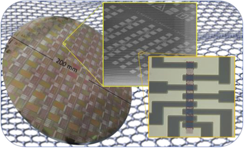
Starting from 2004, the plausibility of isolating a solitary layer of graphite with a thickness of one-atom, so-called graphene, has been experimentally exhibited by mechanical exfoliation of graphite.1 This disclosure is viewed as an achievement in the nanotechnology era, bringing the idea of single atomic components nearer to the real world. Since the identification of the properties of graphene, a relevant number of potential applications have been discussed. Scientists and technologists have immediately taken advantage of graphene’s unprecedented properties for several applications such as gas sensors,2 photodetectors,3,4 solar cells,5 heterojunctions,4 field-effect transistors,6,7 flexible electronics,8 and antennas.9 However, the introduction of a new material has to face several challenges and often requires the development and implementation of new processes to maintain and use the physical properties of the new material in an efficient way. Important progress was made in the field of graphene synthesis; however, considering the constraints of the manufacturability, the properties of graphene and graphene-based devices drastically downgrade in real devices. Furthermore, large-scale and low-cost manufacture is required and for this purpose chemical vapor deposition (CVD) is often used. The most commonly used substrates for graphene growth are transition metals such as Ni10 and Cu.11 Anyway, metallic contamination caused by this manufacturing method can significantly alter the electronic and electrochemical properties of graphene and it forbids the front-end-of-line compatibility in silicon integrated circuit (IC) manufacturing.12 The introduction of germanium as a substrate, besides the elimination of the risk of metallic contamination, implies several additional advantages: (i) low solubility of carbon in Ge enabling the growth of complete monolayer graphene,13 (ii) availability of a large 200 mm single-crystal Ge surface, obtained through epitaxial growth of Ge on Si,14 (iii) the small difference in thermal expansion coefficients between Ge and graphene, which suppresses intrinsic wrinkle formation.15 Exploiting CVD-grown graphene for electronic applications requires a transfer process from the catalyst substrate used for synthesis to a dielectric substrate.16 Besides, the encapsulation of graphene for further processing while maintaining its properties poses a challenge that was already faced in a previous paper.17 However, the performance of graphene-based devices is limited primarily by the large and highly varying contact resistance, RC, that occurs when graphene is brought into contact with a metal.18–20 The carrier injection from metal to graphene is strongly limited by the small density of states (DOS) near the Dirac point. Several approaches have been reported in the last few years to reduce the contact resistance. The following strategies are worth mentioning: the exploration of different device architectures, like metal-on-bottom architecture (MOBA)21 and double contact (sandwiched) geometry22 to take advantage of a cleaner contact area and a wider contact area, respectively; the application of post-processing treatments like annealing23 to activate and promote the otherwise non-contributing dangling bonds; and the introduction of edge contacts24–27 to exploit the contribution of px and py orbitals besides the pz contacted in a top-contact approach.
This work aims to investigate several approaches to find a reliable contact formation process and to study the effects of passivation and patterning of graphene on the contact resistance. We intend to achieve this goal exploiting the tools and processes applied in IC manufacturing in a 200 mm wafer Si technology environment. We present insights into the processes of cleaning, patterning, encapsulating and contacting graphene in a 200 mm wafer pilot line routinely used for the fabrication of ICs in 0.13/0.25 μm SiGe BiCMOS (bipolar-complementary metal–oxide–semiconductor) technologies.
1. Experimental
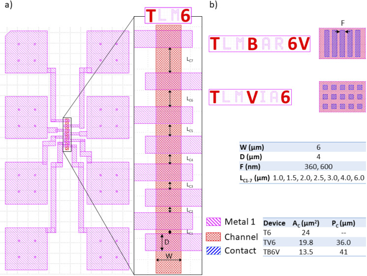
In this section, the experimental details of the modules used for the fabrication of TLM structures are described. The TLM devices (Fig. 1a), used for the extraction of contact resistance, sheet resistance and transfer length (Lt), have a channel width (W) of 6 μm, a contact length (D) of 4 μm and contact separations (LC) ranging between 1 and 6 μm. The patterns used for the realization of the contacts are shown in Fig. 1b, where also the contact areas and perimeters for each structure are provided. Two dissimilar patterns are used.
Fig. 1. In (a) the layout consisting of the layers Channel and Metal 1 can be seen. Two magnifications are shown, one showing the whole device with the Metal 1 pads and the other focusing on the channel. This represents the device TLM6 (T6) as it is processed in the process flow Direct Conventional (DC) i.e. without the layer Contact, used to introduce the patterns. In (b) the layer Contact, used in the process flow Direct Holey (DH) and Passivated Holey (PH), is shown for the devices reported in this work. On the left side of (b) the names of the devices are shown and their abbreviations that will be used below are highlighted in red, e.g. the TLM structure with vertical bars will appear in the text as TB6V. On the bottom side of (b) the legend of the layers and the contact dimensions as well as the contact area (AC) and perimeter (PC) provided by each structure are listed.
1.1. Graphene module
The growth of monolayer graphene by chemical vapor deposition on Ge (0 0 1)/Si (0 0 1) substrates was performed by using an Aixtron Black Magic BM300T. Two micron thick Ge was grown with low pressure epitaxy in an Epsilon 3000 equipment from ASM.28 Due to the very fast diffusion of Si into Ge, the thickness of 2 μm is chosen in order to avoid the formation of SiC clusters during graphene growth at high temperature.29 Graphene synthesis was carried out at a deposition temperature of 885 °C using CH4 as a source of carbon and an Ar/H2 mixture as a carrier gas. A pressure of 700 mbar was kept during the deposition and the deposition time was 60 minutes.30 Ge substrates fully covered by graphene were used as the donor wafer for a PMMA-assisted electrochemical delamination transfer31 to 200 mm SiO2/Si target wafers. The transfer is carried out in a NaOH electrolyte solution where PMMA/graphene/Ge/Si acts as the cathode and a graphite plate as the anode. Following the transfer, a thermal treatment (annealing at 135 °C in N2 and NH3 atmosphere) for water elimination was implemented and chemical processing in acetone was performed for PMMA removal.17
1.2. Passivation module
For the passivation, a silicon nitride/silicon oxide stack was used. The low RF power plasma-enhanced chemical vapor deposition (PECVD) used for the nitride deposition was performed in an Applied Materials Silane DxZ chamber, in which a gas mixture of SiH4/NH3 at 400 °C was introduced. The stoichiometry of the nitride formed is approximately Si10N9H1. For the sake of simplicity, we will refer to it as SiN from now on. PECVD has the advantage of gas phase reactions, which makes it independent from contact catalysis at the surface of graphene. Low RF power is needed to avoid damage to the sp2 network of graphene32 and Raman spectra, taken before and after deposition, showed no influence of SiN deposition on graphene as extensively discussed by Lisker et al.17 The high reproducibility, the across-wafer and wafer-to-wafer uniformity of thickness, and the low impact of its deposition as revealed by Raman spectra made this process the standard graphene passivation process at IHP.
1.3. Contact module
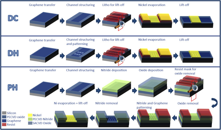
We introduce 3 different contact modules fabricated using a metal-on-top-architecture (MOTA). All the process flows are summarized in Fig. 2. The differences in their design are introduced to highlight the impact of patterns etched in graphene and of the passivation layer applied on graphene. The different process flows will be indicated using a nomenclature composed of 2 letters, describing: (i) the type of contact referring to whether the contact is formed either in a direct (D for Direct) way or exploiting a passivation (P for Passivated) and (ii) defining the presence (H for Holey) or absence (C for Conventional) of patterns etched into the graphene. The following steps are common to all the process flows: the graphene synthesis by CVD on a Ge substrate (donor wafer); the SiO2 deposition on a Si substrate (target wafer) by PECVD from tetraethyl orthosilicate (TEOS) precursors; the transfer of the graphene from the donor to the target wafer performed as explained in Section 1.1; the structuring of the graphene channel by means of an i-line (λ = 365 nm) photolithography step and an Ar/O2 reactive ion etching (RIE) step. The contact is pursued with evaporated nickel and all the samples were treated with post-processing annealing at 250 °C in a nitrogen atmosphere for 600 s.
Fig. 2. Scheme of the 3 process flows exploiting a metal-on-top architecture, starting from the transfer up to the contact formation. The initial steps common to all the process flows and the final annealing step are not shown here.
1.3.1. Direct Conventional
This is the only flow that involves only two masks. The two layers involved are those shown in Fig. 1a: Channel and Metal 1. The lack of the layer contact leads to the fabrication of only one type of device i.e. T6. After the structuring step, the photolithography step for contact formation is performed. The contact is formed by resistive thermal evaporation of ∼30 nm of Ni and the subsequent lift-off process in acetone with ultrasonic agitation.
1.3.2. Direct Holey
This process flow differs from the previous one only by the introduction of patterns in graphene. During the structuring photolithography step, a double exposure with two different masks, Channel and Contact, is performed. The mentioned patterns are squares (TV6) and bars (TB6V) and the latter are placed parallel to the channel length as shown in Fig. 1b. The minimum feature sizes (F) used here are 360 and 600 nm.
1.3.3. Passivated Holey
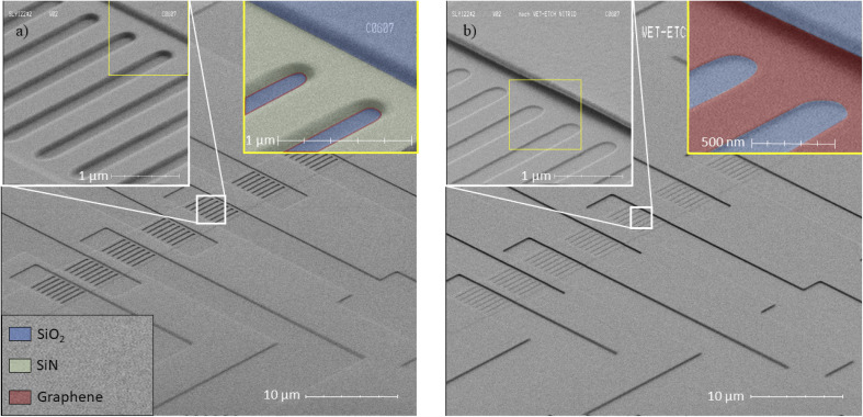
Following the graphene structuring step, a 100 nm thick SiN layer is deposited under the conditions previously mentioned and it is afterwards covered by 100 nm SiO2. The undoped silicate glass (USG) is deposited by sub-atmospheric chemical vapor deposition (SACVD) and it is immediately etched out in the contact region through reactive ion etching. A selective recipe consisting of Ar, C4F8, CF4 and CO ensures that underlying SiN is not cleared away. After a deep UV (DUV, λ = 248 nm) photolithography step, patterns in the graphene (Fig. 3a) are dry-etched through the nitride layer exploiting a fluorinated hydrocarbon-based recipe for RIE involving CHF3 and CF4. The remaining silicon nitride is finally removed exploiting a wet-etch in hot phosphoric acid for 300 s at 160 °C (Fig. 3b). In this step the oxide layer, still present elsewhere than in the contact window, acts as a hard mask to prevent the removal of the passivation layer protecting the channels. This is the most critical step: the etching must last long enough to remove completely the passivation from the contact region in order to take full advantage of the contact area; on the other hand, a too long etching would lead to excessive underetching. The latter obviously occurs due to the isotropical nature of wet-etching and it is clearly visible in the scanning electron microscope image shown in Fig. 3b. The etching rate of SiN was studied on a dummy wafer resulting in ∼40 nm min−1 and an underetching of ∼200 nm is estimated. Prior to H3PO4-based etching a 30 second HF bath was applied for native oxide removal. The metallization is finally pursued through an acetone lift-off process where the contact metal is Ni deposited by resistive thermal evaporation.
Fig. 3. Scanning electron microscope image of a TLM structure (a) after the introduction of patterns in graphene through the SiN passivation layer and (b) after the wet-etch removal of SiN. Insets show the magnifications of the patterns in the contact region. The shown structure is 6 μm wide. The patterns are vertical bars with a minimum feature size of 360 nm.
2. Results
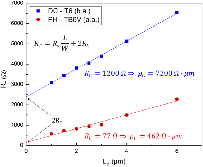
The electrical characterization was performed using a microprobe station at room temperature and atmospheric pressure. I–V characteristics were acquired by applying a voltage sweep from 0 V to 1 V between all the adjacent contacts. For each variant of each process flow, up to 10 devices were characterized prior to and following the annealing process. Contact resistance and sheet resistance were extracted by transmission line measurement, i.e. plotting the resistances as a function of the channel lengths and extracting the contact resistance and the sheet resistance respectively from the intercept and the slope. In Fig. 4 two TLM characteristics are shown. These belong to a T6 device processed with the DC flow (in blue) and to the TB6V device processed with the PH flow, which showed the lowest contact resistance within this work (in red). Hence, the blue curve represents the contact resistance achievable with the graphene we synthesize when the precautions presented in the previous section are not exploited (ρC = 7200 Ω μm) while the red curve represents the best result of this work (ρC = 462 Ω μm). In Table 1 the most remarkable results achieved after the annealing process for each process flow are shown and will be discussed in the next section. The lowest contact resistance obtained in this work is provided by the Passivated Holey process flow. The pattern consisting of vertical bars achieved on average a contact resistance of 110 Ω for a 6 μm wide device.
Fig. 4. TLM characteristics from which the contact resistance and sheet resistance of two devices have been extracted. In blue the device without patterns, T6, processed with the process flow DC and measured before annealing (b.a.). In red the TB6V device processed with PH and measured after the annealing (a.a.) that showed the lowest contact resistance within this work.
Contact resistivity and sheet resistance are reported for all the presented process flows. Measured devices have W = 6 μm. Values obtained after annealing at T = 250 °C for 600 s.
| Sample | ρ C (Ω μm) | R S (kΩ/□) | γ (%) |
|---|---|---|---|
| DC | 2300 | 1.8 | 100 |
| DH | 1100 | 2.3 | 28 |
| PH | 660 | 1.8 | 100 |
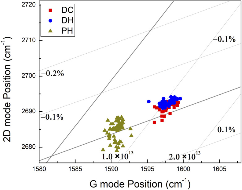
Raman spectroscopy mapping has been performed on channel areas, i.e. on exposed graphene for DC and DH and on passivated graphene for PH. Fig. 5 sums up the correlation analysis of 2D–G mode positions for the three different process flows. This type of analysis enables distinguishing between doping- and strain-related Raman band shifts.33 The first relevant result of such analysis concerns the doping level in graphene and it is based on the comparison of 2D and G band positions for samples differently processed. It can be seen that the doping levels are identical and they are (1.17 ± 0.07) × 1013 cm−2 and (1.18 ± 0.06) × 1013 cm−2 after DC and DH processes respectively whereas the PH process reduced the doping to (0.62 ± 0.04) × 1013 cm−2. It is worth noting that the distribution of PH doping values is narrower than that resulting from the other processes reflecting the fact that the introduction of a passivation layer reduces the distribution range of doping levels. The second observation based on Fig. 5 regards the strain in the graphene layer. According to the correlation analysis, the passivation leads to a slight decrease in the average compressive strain in the graphene layer which, however, falls within the error.
Fig. 5. Correlation analysis of 2D–G mode positions before and after encapsulation.
3. Discussion
At first glance, we can see in Table 1 that the introduction of patterns halves the contact resistance but causes also a drastic decrease in the process yield (γ), from 100% of DC to 28% of DH. The addition of a passivation layer further decreases the contact resistance by a factor of almost 2 and leads to a process yield of 100%. The decreased process yield of DH is to be attributed to the diminished adhesion between graphene and the substrate due to the introduction of the patterns. This is detrimental during the cleaning processes following the structuring and patterning lithography step. The solution of introducing the patterns through the passivation layer, undertaken in the PH flow, allows us to avoid such inconvenience and to increase the process yield. These results, along with the importance of both patterns and passivation, highlight the necessity of the latter.
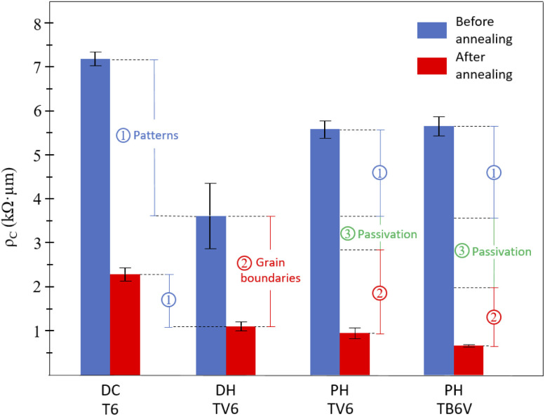
Let us now compare the results, before and after the annealing, of 6 μm wide TLM structures (T6) processed through the Direct Conventional process flow with the results of 6 μm wide squared-patterned structures (TV6) processed with both DH and PH. They correspond to the first 3 bar pairs on the left side of Fig. 6. The results achieved prior to annealing reveal an increase of contact resistance in the passivated samples (PH) with respect to the DH ones as shown by the corresponding blue bars. This higher contact resistance is accompanied by a significantly higher impact, with respect to DC and DH, of the annealing process on the contact resistance, as highlighted by the ratio of blue bars to red bars. Through annealing of the PH samples, the contact resistance decreased by a factor of ∼6, whereas in DC and DH it decreases by a factor of ∼3. It is worth noting that all samples were prepared by using graphene from the same growth process. Therefore, they have the same degree of crystallinity, and hence a similar grain size and similar grain boundary perimeter, i.e. a similar number of dangling bonds. According to Leong et al. and the suggested dissolution-precipitation mechanism, the magnitude of the improvement of the contact resistance upon annealing is directly related to the number of available dangling bonds. Hence, the 3 times lower contact resistivity measured for both DC and DH after the annealing process must be associated with the trigger of the dissolution–precipitation mechanism involving only the dangling bonds provided by the grain boundaries (contribution 2 in Fig. 6), these being the only dangling bonds involved in both samples. Given this consideration, the difference in contact resistivity between DC and DH prior to annealing can be associated entirely with the introduction of patterns (contribution 1 in Fig. 6). This contribution is obviously recognizable also comparing the DC and DH resistivities following the annealing process, i.e. the ratio of blue bars between DC and DH is equal to the ratio of red bars between these two process flows. The dangling bonds provided by the patterns, due to their easily accessible size compared to the grain boundary ones, do not need an activation energy.
Fig. 6. Contact resistivity values with the corresponding deviations before (blue) and after (red) annealing for top contacted samples. For each process flow, results corresponding to a given 6 μm wide test structure are shown. For PH two different test structures are visible. The contributions brought about by the introduction of patterns (contribution 1), the activation of the dangling bonds provided by the grain boundaries (2) and the passivation layer (3) are shown, respectively, in blue, in red and in green. The reintroduction of the pattern contribution in PH samples is based on the contact resistivities of DH samples having the same patterns.
Although experimental evidence is still to be produced, we propose the following process-related hypothesis for the higher resistance reported for PH with respect to DH prior to annealing. Assuming that in PH not only a fraction of grain boundary dangling bonds are saturated, but also some of the dangling bonds introduced by the patterns, the contribution of both the contact area (AC) and the contact perimeter (PC) prior to annealing will be only partial and, furthermore, the annealing process will face the activation of a significantly higher number of dangling bonds with respect to DC and DH cases. That is why a saturation of a portion of pattern dangling bonds in addition to a higher fraction of the grain boundary dangling bonds, due to H atoms coming from the phosphoric acid used during silicon nitride wet etching, may explain both the higher contact resistivity and the higher impact of annealing on it.
In Fig. 6, on the PH bars, the expected pattern contribution was reintroduced and, by considering said enhancement of ρC by a factor of ∼3 due to the annealing step, the contribution provided by the passivation layer (contribution 3, in green), resulting in an additional reduction of ρC, was determined.
The two Holey process flows provided the lowest resistances, shown in Table 2, for two different structures: DH showed lower contact resistance in devices with squares (TV6) while PH showed lower contact resistance in devices with vertical bars (TB6V). It is worth noting that TB6V provides a contact area AC = 13.5 μm2 and a contact perimeter PC = 41.0 μm whereas the area and perimeter provided by TV6 are AC = 19.8 μm2 and PC = 36.0 μm. This means that, although they provide a similar amount of contact perimeter, in the case of vertical bars ∼44% of the graphene has been removed while in the case of squares only ∼18% of the graphene has been removed. Before the annealing these two structures show comparable values of contact resistance both when processed with the DH process flow and with PH, supporting the hypothesis that before the annealing the dominant contribution is brought about by the pattern and hence by PC. After the annealing, in the DH samples the square-patterned devices show half the contact resistance shown by the bar-patterned ones showing that, for a given PC, a wider contact area, once activated, brings about lower contact resistance as expected. In the PH samples this does not occur. The two structures show an opposite trend, with respect to the DH flow, following the annealing treatment. Moreover, TV6 results for the two flows are comparable. Let us assume that a portion of dangling bonds remain saturated even after the annealing process in PH samples due to non-ideal annealing conditions for such a process flow involving the mentioned wet etching.
Contact resistivities before (ρCb.a.) and after (ρCa.a.) the annealing treatment of two devices: 6 μm wide TLM structures with squares (TV6) and with vertical bars (TB6V) processed with both DH and PH process flows.
| ρ Cb.a. (kΩ μm) | ρ Ca.a. (kΩ μm) | |||
|---|---|---|---|---|
| TV6 | TB6V | TV6 | TB6V | |
| DH | 3.60 | 3.59 | 1.09 | 2.28 |
| PH | 5.55 | 5.62 | 0.95 | 0.66 |
Let also assume that, given fixed annealing time and temperature, the probability for this residual saturation, and hence the saturation percentage, is proportional to AC and PC. In this case, the previously mentioned hypothesis could also explain why in PH, given comparable contact perimeters, the lowest resistance is not achieved by the device with the widest AC (TV6) since this shows a higher percentage of process-induced residual saturation due to the wider contact area. This means that even though the introduced passivation is clearly beneficial in terms of both yield and contact resistance, the latter especially for TB6V as shown in Fig. 6, either the wet etching step involved in such a module or the annealing conditions or both are critical and do not allow an efficient exploitation of the whole contact area.
4. Conclusions
In this work, three process flows for the realization of contact between graphene and metal have been designed, developed and characterized in order to optimize the formation of such contact in terms of contact resistance, sheet resistance and yield of the process. The contact module of graphene device fabrication in a 200 mm wafer Si technology environment is introduced with key process steps which may pave the way to large-scale manufacturing of hybrid graphene-Si components.
The top contact with evaporated nickel has been investigated exploiting a conventional approach (DC), a patterned approach (DH) and a patterned approach with passivation (PH). The latter one provided the best result achieved within this work with a contact resistance of 110 Ω, corresponding to ρC = 660 Ω μm, with a process yield of 100%. Such results were achieved by introducing three key factors: (i) the patterns etched in the graphene decrease RC to 50% of the initial value; (ii) the passivation layer contributes to achieving a resistance that is slightly more than half that of the not-passivated samples (in the TB6V case) and the implementation of the patterning of graphene through the passivation layer increased the device yield from 28% of DH to 100% of PH; (iii) the annealing process contributes to decreasing the contact resistance to one third that of non-annealed samples. The introduction of these three features led to a contact resistivity that is only 9% of the contact resistivity measured for a Direct Conventional contact where no post-processing treatments were performed. Further development is needed to further decrease the contact resistance. For instance, each of these 3 factors introduced here needs optimization: (i) optimized geometrical parameters could be designed; (ii) further studies on the annealing process in order to find even better conditions could be done; (iii) a wet etch process for SiN removal that exploits lower concentrations of H could be investigated to confirm the proposed mechanism and, in case, to intervene in passivation module optimization.
Nevertheless, the practical relevance of such a contact module is emphasized by the facts that (i) the proposed materials and processes provide high yield and low-resistance contacts and (ii) are compatible with those used in the large-scale fabrication of Si-based ICs.
Conflicts of interest
There are no conflicts to declare.
Supplementary Material
Acknowledgments
This research was funded by the Federal Ministry of Education and Research (BMBF) Germany under grant GIMMIK No 03XP0210E and the European Union's Horizon 2020 research and innovation programme under Graphene Flagship grant agreement No. 952792.
References
- Novoselov K. S. Geim A. K. Morozov S. V. Jiang D. Zhang Y. Dubonos S. V. Grigorieva I. V. Firsov A. A. Science. 2004;306:666–669. doi: 10.1126/science.1102896. [DOI] [PubMed] [Google Scholar]
- Schedin F. Geim A. K. Morozov S. V. Hill E. Blake P. Katsnelson M. Novoselov K. S. Nat. Mater. 2007;6:652–655. doi: 10.1038/nmat1967. [DOI] [PubMed] [Google Scholar]
- Xia F. Mueller T. Lin Y.-m. Valdes-Garcia A. Avouris P. Nat. Nanotechnol. 2009;4:839–843. doi: 10.1038/nnano.2009.292. [DOI] [PubMed] [Google Scholar]
- Di Bartolomeo A. Giubileo F. Luongo G. Iemmo L. Martucciello N. Niu G. Fraschke M. Skibitzki O. Schroeder T. Lupina G. 2D Mater. 2016;4:015024. doi: 10.1088/2053-1583/4/1/015024. [DOI] [Google Scholar]
- Li X. Zhu H. Wang K. Cao A. Wei J. Li C. Jia Y. Li Z. Li X. Wu D. Adv. Mater. 2010;22:2743–2748. doi: 10.1002/adma.200904383. [DOI] [PubMed] [Google Scholar]
- Schwierz F. Nat. Nanotechnol. 2010;5:487. doi: 10.1038/nnano.2010.89. [DOI] [PubMed] [Google Scholar]
- Di Bartolomeo A. Giubileo F. Iemmo L. Romeo F. Russo S. Unal S. Passacantando M. Grossi V. Cucolo A. M. Appl. Phys. Lett. 2016;109:023510. doi: 10.1063/1.4958618. [DOI] [Google Scholar]
- Eda G. Fanchini G. Chhowalla M. Nat. Nanotechnol. 2008;3:270–274. doi: 10.1038/nnano.2008.83. [DOI] [PubMed] [Google Scholar]
- Jornet J. M. Akyildiz I. F. IEEE J. Sel. Areas Commun. 2013;31:685–694. [Google Scholar]
- Yu Q. Lian J. Siriponglert S. Li H. Chen Y. P. Pei S.-S. Appl. Phys. Lett. 2008;93:113103. doi: 10.1063/1.2982585. [DOI] [Google Scholar]
- Li X. Cai W. An J. Kim S. Nah J. Yang D. Piner R. Velamakanni A. Jung I. Tutuc E. et al. . Science. 2009;324:1312–1314. doi: 10.1126/science.1171245. [DOI] [PubMed] [Google Scholar]
- Lupina G. Kitzmann J. Costina I. Lukosius M. Wenger C. Wolff A. Vaziri S. Ostling M. Pasternak I. Krajewska A. et al. . ACS Nano. 2015;9:4776–4785. doi: 10.1021/acsnano.5b01261. [DOI] [PubMed] [Google Scholar]
- Wang G. Zhang M. Zhu Y. Ding G. Jiang D. Guo Q. Liu S. Xie X. Chu P. K. Di Z. et al. . Sci. Rep. 2013;3:2465. doi: 10.1038/srep02465. [DOI] [PMC free article] [PubMed] [Google Scholar]
- Lee J.-H. Lee E. K. Joo W.-J. Jang Y. Kim B.-S. Lim J. Y. Choi S.-H. Ahn S. J. Ahn J. R. Park M.-H. et al. . Science. 2014;344:286–289. doi: 10.1126/science.1252268. [DOI] [PubMed] [Google Scholar]
- Bao W. Miao F. Chen Z. Zhang H. Jang W. Dames C. Lau C. N. Nat. Nanotechnol. 2009;4:562–566. doi: 10.1038/nnano.2009.191. [DOI] [PubMed] [Google Scholar]
- Lee H. C. Liu W.-W. Chai S.-P. Mohamed A. R. Aziz A. Khe C.-S. Hidayah N. M. Hashim U. RSC Adv. 2017;7:15644–15693. doi: 10.1039/C7RA00392G. [DOI] [Google Scholar]
- Lisker M. Lukosius M. Fraschke M. Kitzmann J. Dabrowski J. Fursenko O. Kulse P. Schulz K. Krüger A. Drews J. Schulze S. Wolansky D. Schubert A. Katzer J. Stolarek D. Costina I. Wolff A. Dziallas G. Coccetti F. Mai A. Microelectron. Eng. 2018;205:44–52. doi: 10.1016/j.mee.2018.11.007. [DOI] [Google Scholar]
- Xia F. Perebeinos V. Lin Y.-m. Wu Y. Avouris P. Nat. Nanotechnol. 2011;6:179–184. doi: 10.1038/nnano.2011.6. [DOI] [PubMed] [Google Scholar]
- Russo S. Craciun M. Yamamoto M. Morpurgo A. Tarucha S. Physica E: Low-Dimensional Systems & Nanostructures. 2010;42:677–679. [Google Scholar]
- Nagashio K. Toriumi A. Jpn. J. Appl. Phys. 2011;50:070108. doi: 10.1143/JJAP.50.070108. [DOI] [Google Scholar]
- Bharadwaj B. K. Nath D. Pratap R. Raghavan S. Nanotechnology. 2016;27:205705. doi: 10.1088/0957-4484/27/20/205705. [DOI] [PubMed] [Google Scholar]
- Franklin A. D. Han S.-J. Bol A. A. Perebeinos V. IEEE Electron Device Lett. 2011;33:17–19. [Google Scholar]
- Leong W. S. Nai C. T. Thong J. T. Nano Lett. 2014;14:3840–3847. doi: 10.1021/nl500999r. [DOI] [PubMed] [Google Scholar]
- Smith J. T. Franklin A. D. Farmer D. B. Dimitrakopoulos C. D. ACS Nano. 2013;7:3661–3667. doi: 10.1021/nn400671z. [DOI] [PubMed] [Google Scholar]
- Park H.-Y. Jung W.-S. Kang D.-H. Jeon J. Yoo G. Park Y. Lee J. Jang Y. H. Lee J. Park S. et al. . Adv. Mater. 2016;28:864–870. doi: 10.1002/adma.201503715. [DOI] [PubMed] [Google Scholar]
- Anzi L. Mansouri A. Pedrinazzi P. Guerriero E. Fiocco M. Pesquera A. Centeno A. Zurutuza A. Behnam A. Carrion E. A. et al. . 2D Mater. 2018;5:025014. doi: 10.1088/2053-1583/aaab96. [DOI] [Google Scholar]
- Passi V. Gahoi A. Marin E. G. Cusati T. Fortunelli A. Iannaccone G. Fiori G. Lemme M. C. Adv. Mater. Interfaces. 2019;6:1801285. doi: 10.1002/admi.201801285. [DOI] [Google Scholar]
- Yamamoto Y. Zaumseil P. Arguirov T. Kittler M. Tillack B. Solid-State Electron. 2011;60:2–6. doi: 10.1016/j.sse.2011.01.032. [DOI] [Google Scholar]
- Lupina G. Lukosius M. Lippert G. Dabrowski J. Kitzmann J. Lisker M. Kulse P. Krueger A. Fursenko O. Costina I. et al. . ECS J. Solid State Sci. Technol. 2017;6:M55. doi: 10.1149/2.0141705jss. [DOI] [Google Scholar]
- Lukosius M. Dabrowski J. Kitzmann J. Fursenko O. Akhtar F. Lisker M. Lippert G. Schulze S. Yamamoto Y. Schubert M. A. Krause H. M. Wolff A. Mai A. Schroeder T. Lupina G. ACS Appl. Mater. Interfaces. 2016;8:33786–33793. doi: 10.1021/acsami.6b11397. [DOI] [PubMed] [Google Scholar]
- Lukose R. Lisker M. Akhtar F. Fraschke M. Grabolla T. Mai A. Lukosius M. Sci. Rep. 2021;11:1–10. doi: 10.1038/s41598-020-79139-8. [DOI] [PMC free article] [PubMed] [Google Scholar]
- Ahlberg P. Johansson F. Zhang Z.-B. Jansson U. Zhang S.-L. Lindblad A. Nyberg T. APL Mater. 2016;4:046104. doi: 10.1063/1.4945587. [DOI] [Google Scholar]
- Lee J. E. Ahn G. Shim J. Lee Y. S. Ryu S. Nat. Commun. 2012;3:1–8. doi: 10.1038/ncomms2022. [DOI] [PubMed] [Google Scholar]


