Abstract
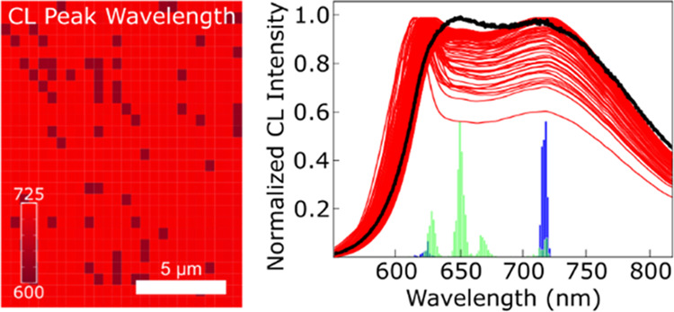
Full-spectrum cathodoluminescence (CL) mapping provides a point-by-point spatial measurement of the apparent band gap of a semiconductor thin film. In most studies, analysis of the electrical film properties from CL is presented as color mapping images. We have developed a spectra data analysis algorithm to functionalize, analyze, and generate statistical measurements of the luminescence data to provide additional insights. This algorithm was coded in the R language program, and a set of CdMgSeTe films were studied as an application case study. CL maps were measured for samples with different luminescent responses. A quantitative measure of the heterogeneity of the films was generated by statistical analysis of luminescent intensity and wavelength, spectra type curves, frequency distributions of peak wavelength, and relative intensity maps. The final CL analysis facilitates the investigation of the CdMgSeTe films and has potential applications for many semiconductor films.
Introduction
Cathodoluminescence (CL) spectroscopy is a nondestructive in situ microscopy characterization and mapping technique where emitted luminescence formed from the recombination of electron/hole pairs is collected from the sample during electron beam excitation.1,2 The emission can be measured to provide an approximate measurement of the apparent local band gap in a semiconductor.3,4 Thin-film semiconductor layers are central to a wide range of devices,5−9 and CL mapping can be collected to determine apparent band-gap variations across the film, which can degrade performance such as photovoltaic (PV) efficiency.10,11 However, large data sets are generated during dense full-spectrum CL mapping,12 and analysis either limits data set size or reduces analysis to a color map.3,13−15
A deeper analysis of the CL mapping would enable quantitative insight into the films. For instance, characterization of the homogeneity of the band gap is needed when the substitution of same-group elements into a semiconductor film is used for tuning the absorption and electrical properties of photovoltaics.16,17 This type of element substitution is used to fabricate wide band-gap CdTe photovoltaics as potential top layers of low-cost CdTe/Si tandem cells.18 One method to create wide band-gap CdTe alloys is the cosublimation of Mg with CdTe or CdSeTe.18−21 Characterization of the resulting films by CL is a direct measurement of the apparent band gap and, in this specific case, a proxy for difficult-to-measure composition.
The most common nondestructive method for compositional measurement is energy dispersive spectroscopy (EDS). EDS is often used to predict various properties, including the band gap, based on the measured composition. However, detection of lighter elements is limited due to fewer X-ray signals, leading to poor signal-to-noise,22 and some elements, such as Mg and Se, have a signal overlap.4 In these situations, CL experiments can be used as a complement to EDS analysis for composition information.
Here, we utilize CL to provide quantitative insight into the degree of homogeneity of CdMgSeTe thin films. We find that the Mg crucible temperature during film sublimation determines the apparent band gap and homogeneity of the resulting film. Films with Mg targets at the midpoint of the set show a single luminescence peak. Films with a high or low Mg target composition, and thus a high or low Mg crucible temperature, show bimodal luminescent spectra, suggesting phase segregation. Luminescence mapping and a custom-written R language program are used to analyze the mapping data sets for the normalized intensity and peak wavelength at maximum intensity (λp). This analysis confirms the bimodal nature of some of the wide-area luminescence measurements and provides a quantitative measure of the heterogeneity of the films using λp histograms and type curves of the mapped spectra. These same techniques could be applied to other thin-film devices, making this a valuable case study into the uses of spatial CL measurements and analysis.
Experimental Details
Methods
Cd(1–x)Mg(x)Se(y)Te(1–y) (CdMgSeTe) devices were fabricated on TEC10/100 nm MgZnO (MZO) using a two-source custom-made sublimation chamber with CdSe0.05Te0.95 and Mg sources developed at the Colorado State University and described previously.20,23 Higher band-gap materials are targeted by increasing x and y. For this study, the CdSe0.05Te0.95 crucible temperature was maintained at 565 °C during sublimation, while the Mg crucible temperature was varied from 420 to 450 °C in increases of 5 °C. The temperature was increased at this rate to obtain a set of seven Cd(1–x)Mg(x)Se0.05Te0.95 films. The samples were identified as Mg–X, where X corresponds to the sublimation temperature of the Mg crucible.
Characterization
The seven Cd1–xMgxSeyTe1–y films were characterized at room temperature in a JEOL 7610F scanning electron microscope (SEM) equipped with a Horiba cathodoluminescence (CL) detector and an Oxford energy dispersive spectroscopy (EDS) detector. SEM images were obtained using an accelerating voltage of 5–10 kV and a probe current (PC) of 13 μA. Elemental analysis of the thin films was performed an Oxford xMax EDS system with an accelerating voltage of 15 kV and PC of 13. All EDS measurements were taken at a magnification of 5k× to be consistent with the CL cathodoluminescence (CL). EDS mapping of the thin films was collected at an area of 20 × 20 mm2 for a duration of 30 min and a pixel integration of 1 s/pixel.
Cathodoluminescence (CL) measurements were taken using a CCD Syncerity detector on a Horiba Instruments iHR-320 at a spectral range of 500–1100 nm and collected using an accelerating voltage of 30 kV to maximize signal intensity. Full scanned-area CL spectra were obtained for each sample at 10, 20, and 50k×. CL maps were acquired from a 0.5 μm × 0.5 μm grid with 702 points at a magnification of 5k× and an integration time of 1 s/pixel. Integrated heat maps (also called red maps due to their typical coloring) were created and exported from Horiba LabSpec6 software by integrating the intensity over the entire measured luminescence spectrum at each measurement location. All full spectrum and mapping data were collected using a grating of 300 with a slit width of 7 mm. Luminescence was not corrected for detector quantum efficiency because the majority of measurements are between 600 and 835 nm, where the quantum efficiency (QE) is between 50 and 58%.24 The approximate local band gap for each sample was calculated from the wide-area luminescence measurements by dividing hc = 1240 nm·eV by the peak wavelength of the highest energy peak in nanometers. Band gaps were also calculated using the Tauc plot method25 from optical transmittance measurements as described for this class of films previously by Swanson et al.18,19
Data Analysis
Spectral luminescence data at each measurement point were analyzed using a custom-written R program language. An earlier version of the algorithm was described previously with an analysis conducted on a generic photovoltaic cell.26 Each spectrum was functionalized by fitting a spline using the “smooth.spline” function in the “stats”-package to the experimental data points with wavelength as the independent variable and the CL intensity as the dependent variable. The functionalized data were used to find absolute max intensity and wavelength after reparametrizing the function into a piecewise polynomial form (Zheyuan Li, Package: SplineUtils) using the R-package “SplineUtils”. The derivative of this piecewise polynomial is taken and used to solve for the critical maximum values and using the curve′s equation to identify the corresponding intensity and wavelength. The spectra’s coordinates, intensity, normalized intensity, and peak wavelength (λp) are recorded in a table for later use. This routine is performed on all of the spectra, and a data set max is found. Each spectrum’s max intensity is normalized using the data set max. Heat maps are created using the spectra’s coordinates and normalized intensity or peak wavelength.
Results and Discussion
Full-spectrum total scanned-area luminescence for seven CdMgSeTe films is shown for each sample in Figure 1a. The samples are identified as Mg–X, where X corresponds to the sublimation temperature of the Mg crucible. A blue shift in the luminescence peaks is observed as the Mg crucible temperature increases as a likely result of increasing Mg concentration in the CdMgSeTe films. Four sets of CL measurements at different magnifications were taken from all samples, and the data in Figure 1a are representative of all measurements. A general trend of increasing luminescent intensity with increasing Mg crucible temperature was held throughout all measurements, with some intensity perturbations due to equipment variability observed in the Mg-425 to Mg-435 samples. While absolute intensity values depend on measurement conditions, each data set was measured in a single day using identical conditions to provide some validity to qualitative intensity comparison between the samples. The CL response was uncorrected for detector quantum efficiency (QE) since the bulk of the measurements fell in a wavelength range where QE was between 50 and 58%.24 Some of the longer wavelength responses could be depressed due to decreasing efficiency. CL spectra had the same curve shape and wavelength maximum at all magnifications, as shown in Figure 1b,c. Table 1 lists band gaps for each sample calculated from the initial luminescence peak and transmittance measurements. Transmittance spectra used to measure the band gap for Mg-435 and Mg-450 are shown in Figure S1. Band-gap values for each of these samples were estimated from these spectra following the procedure outlined by Swanson et al.18 The bulk band gap of Cd1–xMgxSeyTe1–y devices was measured between 1.57 and 2 eV based on transmittance, and similar measurements are obtained from the CL. While the CL measured local band gaps are slightly lower eV values, both measurements are within the expected range and comparable to each other. The band gap measurements indicate that a Mg/(Cd + Mg) composition ratio in the range of 0.05–0.25 is likely.27
Figure 1.
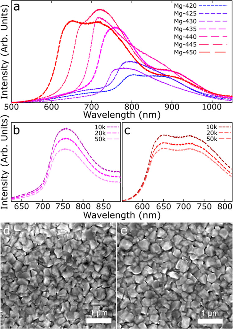
(a) Broad-area CL spectra from the seven CdMgSeTe films with increasing Mg crucible deposition temperature taken at a 20k× magnification. Samples Mg-435 (pink) and Mg-450 (red) were selected for further study, and the measurement line thickened. (b) Mg-435 CL measured at a magnification of 10k× (top, dark pink), 20k× (middle, pink), and 50k× (bottom, light pink). (c) CL of Mg-450 measured at a magnification of 10k× (top, dark red), 20k× (middle, red), and 50k× (bottom, light red). Spatial SEM images from (d) Mg-435 and (e) Mg-450 exhibit no gross morphological differences.
Table 1. Band Gap Calculated from Transmittance and Luminescence Measurementsa.
| transmittance band gap (eV) | CL band gap (eV) | |
|---|---|---|
| Mg-420 | 1.57 | 1.55 |
| Mg-425 | 1.60 | 1.56 |
| Mg-430 | 1.64 | 1.63 |
| Mg-435 | 1.69 | 1.65 |
| Mg-440 | 1.75 | 1.73 |
| Mg-445 | 1.84 | 1.82 |
| Mg-450 | 2.00 | 1.94 |
Band gap determined from the first major peak in the luminescence data.
The luminescence in Figure 1a shows many of the samples exhibit multiple peaks, indicating a high degree of heterogeneity. Two samples, Mg-435 and Mg-450, were selected for further study based on the large-area measurements. Mg-435 is representative of a sample with one primary peak and Mg-450 of two peaks with similar responses. Figure 1d,e shows spatial SEM images exhibiting similar morphology for Mg-435 and Mg-450, consisting of polycrystalline structures with no unique features, making it unlikely differing CL response is due to the morphology of the films. Morphology was similar across all samples, as shown in the SEM images in the supplemental material (Figure S2).
High-density CL maps were generated to determine the variability of the luminescence response by repeating the CL measurement across a large area of the sample in a 0.5 μm × 0.5 μm grid resulting in 702 total spectra collected for each sample. Intensity heat maps in Figure 2a,c are generated by integrating the luminescence signal across the spectra shown in Figure 2b,d. Both films appear to be a random mixture of high- and low-intensity points. The individual spectra given in Figure 2b,d, however, show two potential curve types. In the Mg-435 sample, most curves appear to have a relatively normal distribution around a value of 760 nm, with a few showing strong peaks in the 725–735 nm range. In contrast, the Mg-450 sample shows bimodal spectra with peaks in the 718 and 624 nm range. In most of the spectra, the relative height of the two peaks is similar. Red maps created from spectral integrations across smaller wavelength ranges did not add value to the analysis. Additional data processing, as described below, was needed to quantify and map the data.
Figure 2.
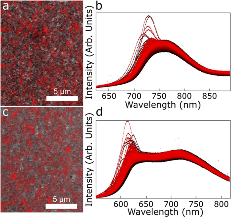
(a, c) Integrated intensity heat maps where darker red indicates higher intensity and (b, d) high-density CL spectra (702 spectra with 1024 points/spectra) of (a, b) Mg-435 and (c, d) Mg-450. Black to red coloring of the individual spectra (c, d) based on the spatial measurement location (starting with black at the top left of the map and ending with red at the bottom right) is added to provide contrast to each individual spectrum.
It can be challenging to gain additional insights from CL mapping due to the large amount of data analysis needed on each spectrum. We have developed an analysis package using the R language to generate additional measurements to analyze and visualize the entire set of luminescence data.23 Each spectrum is splined to smooth measurement variability and functionalize the experimental data. The peak wavelength (λp) is determined by taking the derivative of the splined curve and solving for the global and local maxima. These can be converted into maps or histograms. One of the spectrum from Mg-435 is shown below in Figure 3, with the data points, splined curve, and maxima identified. Functionality is also included to zoom in on any portion of the graph. Representative curves were also analyzed using Gaussian fitting to identify the position of the peak maxima for comparison to the results obtained from the analysis of the spectra as shown in Figure 3. After fitting spectra for Mg-435 and Mg-450 (Figure S3), it was determined that the peak maxima reasonably matched what was identified using the R language program. Further work to introduce Gaussian fitting to all of the curves will be explored.
Figure 3.
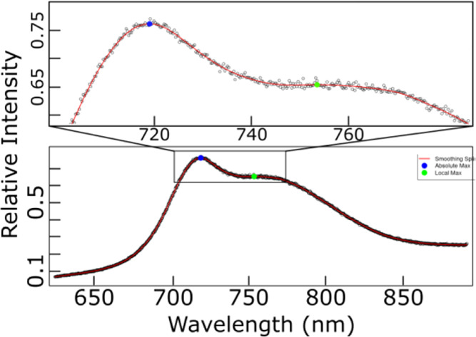
Individual Mg-435 spectrum showing the measured data and splined function of data. The top figure is a zoomed view of the primary peak. The point indicated with a blue circle is the absolute maximum for the spectrum and with the green square is a local maximum.
Figure 4 shows maps of the maximum normalized intensity (a, b), with no integration, and the λp (c, d) from the functionalized spectra. A large degree of homogeneity is seen in both the intensity and λp in the Mg-435 sample based on the visual distribution of the colors. The average (x̅) normalized intensity is 0.62, the standard deviation (σ) is 0.044, and the peak wavelength x̅ = 758.1 nm and σ = 5.8 nm. There is similar homogeneity in the normalized intensity of Mg-450 with x̅ = 0.59 and σ = 0.040, but a high degree of heterogeneity in the λp with x̅ = 708.3 nm and σ = 27.4 nm. Spectra with peak wavelengths at a much lower value are scattered evenly across the film. Blocks of lower λp may indicate phase segregation as the Mg concentration is increased during sublimation. The statistical analyisis of the maximum peak for the samples is summarized in Table 2. Further evidence for potential phase segregation was obtained by performing nondestructive EDS measurements on the CdMgSeTe thin films. Prior reports have measured the Mg content by EDS in Mg-incorporated CdTe;28 however, it is difficult to accurately measure Mg in Cd1–xMgxSeyTe1–y due to the inability of deconvolution of the Mg Kα and Se Lα signals.29 This makes EDS an ineffective tool for determining a quantitative measure of composition for Cd1–xMgxSeyTe1–y thin films. Due to the overlapping of Se and Mg, it was not possible to accurately measure compositional data for these elements. However, it is possible to compare the Mg mapping results from EDS with CL mapping to see if there is a qualitative agreement between the measurements. Although Se and Mg signals overlap, since the Se concentration is set by the CdSeTe crucible concentration and does not change between samples, any changes in the Mg mapping should be attributable to changes in the Mg composition. The similar pattern evident in qualitative maps of CL and EDS in Figure 4c–f is suggestive that a similar distribution of the Mg/Cd ratio is reasonable. EDS spectra for each sample are presented in Figure S4.
Figure 4.
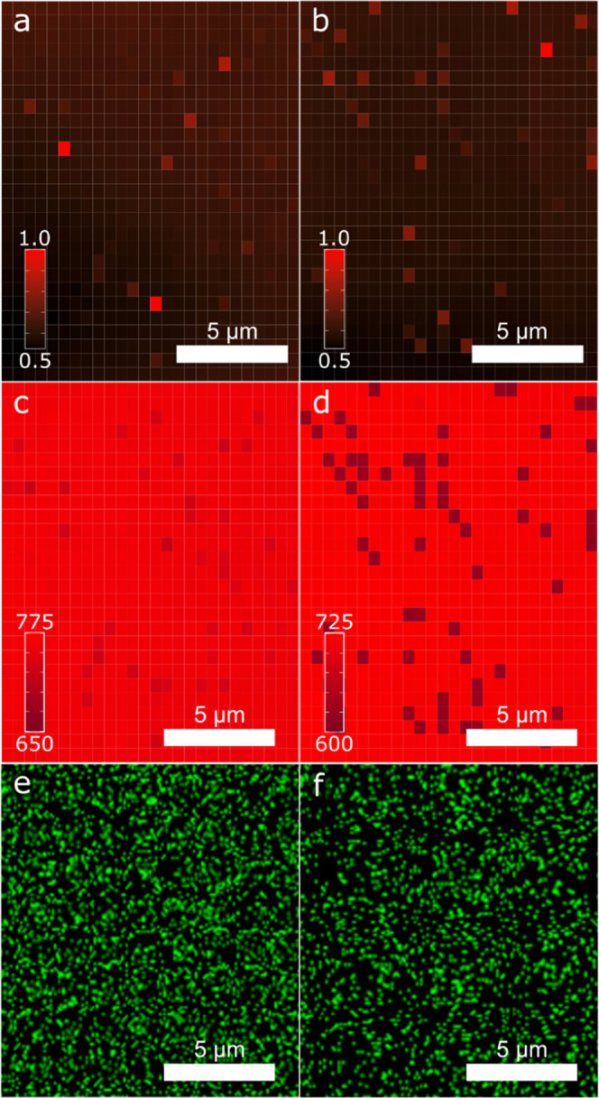
Normalized intensity (a, b) and peak (c, d) wavelength maps for Mg-435 (a, c) and Mg-450 (b, d). The red pigment in the peak wavelength maps is scaled to a 125 nm range to facilitate a direct comparison of the maps. The Mg Kα EDS map for Mg-435 (e) and Mg-450 (f). A similar qualitative pattern is observed in the peak wavelength and EDS maps but is more apparent in the CL data.
Table 2. Mean (x̅) and Standard Deviation (σ) of the Normalized Intensity and Peak Wavelength (λp) for Mg-435 and Mg-450.
| normalized
intensity |
λp (nm) |
|||
|---|---|---|---|---|
| x̅ | σ | x̅ | σ | |
| Mg-435 | 0.62 | 0.044 | 758.1 | 5.8 |
| Mg-450 | 0.59 | 0.040 | 708.3 | 27.4 |
While qualitative images and sample averages are informative, further peak wavelength distribution analysis strengthens the quantification of homogeneity. Distribution analysis is graphically represented using a histogram of the absolute λp of each spectrum, shown in Figure 5 (dark blue blocks). Histograms allow us to quantify the heterogeneity of the luminescence around different wavelengths. Overall, 661 of the 702 spectra in Mg-435 have an absolute λp distributed at around 760 nm. A small subset of 41 spectra exhibits an absolute λp distributed roughly at around 729 nm. The absolute λp for Mg-450 occurs primarily distributed at around 718 nm (637 spectra), but with a larger secondary set distributed at around 624 nm (65 spectra). The functionalized spectra can also be analyzed for any local maxima, allowing us to observe where secondary λp occurs, which are shown in Figure 5 (light green blocks). Particularly striking is that Mg-435 has only 89 local maxima points, compared to 1225 local maxima for Mg-450, owing to the homogeneous and heterogeneous natures of the two samples, respectively. This analysis provides additional support that Mg-450 experiences phase segregation, leading to two strong luminescence peaks at different functional band gaps.
Figure 5.
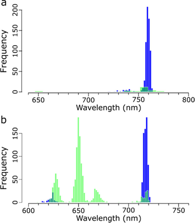
Global (dark blue) and local (light green) maxima for each luminescent spectra measurement for (a) Mg-435 and (b) Mg-450 samples. The x-axis includes appropriate wavelength values for each sample but is kept at a range of 160 nm for comparison purposes.
The spectra can also be visualized by normalizing the curves to create different “type” curves that are representative of each sample. Normalized spectra curves are generated in two fashions. The first is a normalization of each spectral curve in Figure 6a,b by the max set intensity, leading to a graph that looks almost identical to Figure 2b,d, only with functionalized splined curves. The second normalization divides each spectrum by the individual spectrum maximum, i.e., each spectrum has a maximum value of one in normalized intensity. This allows for the shape of each individual curve to be compared in Figure 6c,d. In both cases, the normalized curves indicate that the samples are predominantly one typical type curve. In the case of the Mg-435 sample, most of the curves have a single relatively normal peak centered at around 750 nm, agreeing with the wide-area CL measurement. This peak is present as a shoulder in the atypical measurements of Mg-435; however, there is a secondary peak at 730 nm that is dominant in these curves. This matches the secondary subset of λp seen in the histogram analysis. The Mg-450 sample shows a vastly different type curve with a clear bimodal curve with a broad peak centered at 720 nm and a secondary luminescence peak located at 625–650 nm in almost all samples. The atypical curves in this sample have a vastly larger λp centered at around 624 nm and match the subset of spectra with a peak wavelength in that same region in the histograms. These atypical curves still have a secondary peak at around 720 nm and maintain the same general curve type. These shapes correspond directly with the histograms (added to Figure 6c,d for direct comparison), where peaks line up almost directly with the absolute peak wavelengths of the spectra but with many more curves present at the primary peak wavelengths, as indicated by the darkness of the red curves.
Figure 6.
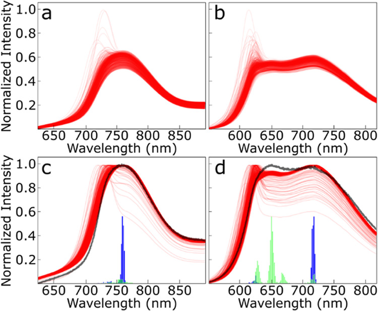
Normalized functionalized spectra for the samples from the Mg-435 (a, c) and Mg-450 (b, d) samples. The functionalized spectra are normalized using the global set maxima intensity (a, b) and the individual spectra intensities (c, d). The density of functionalized spectra is directly proportional to the degree of opacity of the red coloring as spectra are presented at a 15% opacity. The broad-area CL spectra (Figure 1) and the histogram data (Figure 5) were added to the individual spectra normalization.
The wide-area spectral data are overlayed on the normalized type curves in Figure 6c,d. The overlayed curve matches very precisely with the sum of the type curves and the histograms. For Mg-435, this is a normal type curve centered near 750 nm. Mg-450 shows a bimodal curve where the majority of λp at 720 nm causes a major peak in the CL data. The secondary peak observed in the broad-area CL centered at 650 nm is in agreement with the largest grouping of local maxima at 650 nm. Since all data curves have a strong component from 625 to 650 nm with a subset of curves with absolute maxima at 625 nm, the peak at 650 nm has a similar or slightly higher intensity to the 720 nm peak. However, the atypical curves that strongly suggest phase segregation in both Mg-435 and especially in Mg-450 are lost without the additional data analysis from the type curves and histograms and allow us to quantify the heterogeneity of the samples.
Qualitative mapping of the insights from the type curves and histograms can be obtained by mapping the relative intensity between the absolute and local maxima of λp. Figure 7 shows relative intensity maps for the two major absolute λp locations and statistical anlysis of the relative intensity is given in Table 3. The 729/760 nm relative intensity of Mg-435 in Figure 7a has an average of 0.86 and a standard deviation of 0.069. The maximum relative intensity approaches 1.6 for these measurements, indicating a strong divergence of the intensity in some locations. While these areas are atypical, they are likely attributed to areas of high Mg concentration, and although there is a minimum overall correlation between the maximum intensity and wavelength, it does appear that high-intensity measurements are more probable at the secondary peak positioned at 720 nm. Additional correlations between the wavelength and intensity are the subject of future work; however, this aligns with the observation of increasing luminescence with increasing Mg temperature noted in the full area spectra. The Mg-450 624/718 nm relative intensity map in Figure 7b has an average of 0.91 and a standard deviation of 0.073, but with the maximum relative intensity of only 1.3. In contrast to the Mg-435 sample, the Mg-450 sample seems to exhibit phase desegregation in almost all individual spectra measurements. This leads to the relative intensity between the maxima peaks being more evenly distributed, as shown in Figure 7b.
Figure 7.
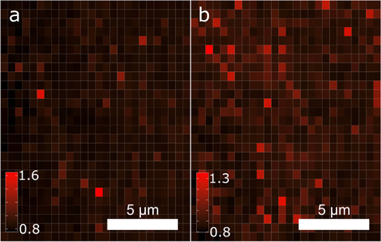
Relative intensity maps of the ratio of the intensity of the first peak/second peak from the absolute peak wavelength histograms of samples (a) Mg-435 (729/760 nm) and (b) Mg-450 (624/718 nm).
Table 3. Mean (x̅) and Standard Deviation (σ) of the Relative Intensity of Luminescent Peaks for Mg-435 and Mg-450.
| x̅ | σ | |
|---|---|---|
| Mg-435 729/760 nm | 0.86 | 0.069 |
| Mg-450 624/718 nm | 0.91 | 0.073 |
| Mg-450 650/718 nm | 0.94 | 0.008 |
In contrast to Mg-435, additional relative intensity maps for Mg-450 can be generated at secondary peaks based on the relative maxima histogram in Figure 5. The most prominent relative maxima peak is located at 650 nm, and a plot of the relative intensity of 650/718 nm can be found in the Supporting Information (Figure S5). The range of the relative intensity is uniform with a relative intensity of x̅ = 0.94 and σ = 0.008. This supports the understanding of the type curves compared to the large-area curves, where most curves feature a primary peak at 718 nm and a secondary peak at 650 nm, as seen in the wide-area CL spectra. It also indicates that the secondary features of Mg-450 have a peak wavelength of ∼624 nm, which is atypical of most of the samples and is highlighted in the 624/718 nm relative intensity curve shown in Figure 7.
Conclusions
Thin films comprised of CdMgSeTe were analyzed using cathodoluminescence (CL) mapping to provide a clear understanding of the band-gap properties of the material as well as a measurement of the homogeneity of that band gap across the surface of the material. These studies helped to overcome the difficulties in using EDS alone as a tool for quantitative and qualitative analysis. Instead, it was observed that CL and EDS mapping can be used as complements for the compositional analysis of devices. The mapping from CL helped to qualitatively show that the Mg-435 film showed more homogeneity than Mg-450. The utilization of the R language allowed for a more streamlined analytical process to visualize the collected luminescence data and measure the local and global maxima. Normalization of the broad spectra curves produced a type curve with each sample showing two distinct types. The relative and global maxima showed to be in good agreement with the type curves once overlayed with normalized spectra. Additionally, quantitative data regarding hetero- and homogeneity can be observed by overlaying the broad CL spectra with the normalized CL spectra and λp histogram. These results show the value of using a technique like CL for quantitative and qualitative analysis of materials. In the case of these CdMgSeTe devices, ongoing work is exploring potential causes of the phase desegregation, and the CL analysis package will be used to show that fabrication modifications were efficacious in reducing heterogeneity. Additionally, further applications for the use of CL can be in quality control of devices or identification of compositional change.
Acknowledgments
The authors would like to thank Dr. Chris Thron for helpful discussions surrounding the analysis and presentation of the luminescence data. The authors acknowledge financial support for this work from the NSF Industry/University Cooperative Research Center on Next Generation Photovoltaics (IIP-1624539, IIP- 1821526) and the Texas A&M System Chancellor’s Research Initiative.
Supporting Information Available
The Supporting Information is available free of charge at https://pubs.acs.org/doi/10.1021/acsomega.2c05640.
Transmittance spectra of Mg-435 and Mg-450; scanning electron images of all CdMgSeTe samples; Gaussian curve fits for two sample spectra; EDS spectra of Mg-435 and Mg-450, and relative intensity map of Mg-450 (PDF)
The authors declare no competing financial interest.
Supplementary Material
References
- Schwarz C.; Chernyak L.; Flitsiy E.. Cathodoluminescence Studies of Electron Injection Effects in Wide-Band-Gap Semiconductors. In Cathodoluminescence; InTech, 2012. [Google Scholar]
- Exner H. E.Qualitive and Quantitative Surface Microscopy. In Physical Metallurgy, 4th ed.; Cahn R. W.; Haasen P., Eds.; North-Holland: Oxford, 1996; pp 943–1032. [Google Scholar]
- Kociak M.; Zagonel L. F. Cathodoluminescence in the Scanning Transmission Electron Microscope. Ultramicroscopy 2017, 176, 112–131. 10.1016/j.ultramic.2017.03.014. [DOI] [PubMed] [Google Scholar]
- Goldstein J. I.; Newberry D. E.; Michael J. R.; Ritchie N. W. M.; Scott J. H. J.; Joy D. C.. Scanning Electron Microscopy and X-Ray Microanalysis, 4th ed.; Springer: New York, 2018. [Google Scholar]
- Frey H.Applications and Developments of Thin Film Technology. In Handbook of Thin-Film Technology; Frey H.; Khan H. R., Eds.; Springer: Berlin, Heidelberg, 2015; pp 1–3. [Google Scholar]
- Handbook of Thin Film Deposition, 3rd ed.; Seshan K., Ed.; William Andrew Publishing: Oxford, 2012. [Google Scholar]
- Lee T. D.; Ebong A. U. A Review of Thin Film Solar Cell Technologies and Challenges. Renewable Sustainable Energy Rev. 2017, 70, 1286–1297. 10.1016/j.rser.2016.12.028. [DOI] [Google Scholar]
- Rahman F. Zinc Oxide Light-Emitting Diodes: A Review. Opt. Eng. 2019, 58, 010901 10.1117/1.OE.58.1.010901. [DOI] [Google Scholar]
- Park J. W.; Kang B. H.; Kim H. J. A Review of Low-Temperature Solution-Processed Metal Oxide Thin-Film Transistors for Flexible Electronics. Adv. Funct. Mater. 2020, 30, 1904632 10.1002/adfm.201904632. [DOI] [Google Scholar]
- Grabitz P. O.; Rau U.; Werner J. H. Modeling of Spatially Inhomogeneous Solar Cells by a Multi-Diode Approach. Phys. Status Solidi A 2005, 202, 2920–2927. 10.1002/pssa.200521205. [DOI] [Google Scholar]
- Punitha K.; Sivakumar R.; Sanjeeviraja C.; Ganesan V. Influence of Post-Deposition Heat Treatment on Optical Properties Derived from UV–Vis of Cadmium Telluride (CdTe) Thin Films Deposited on Amorphous Substrate. Appl. Surf. Sci. 2015, 344, 89–100. 10.1016/j.apsusc.2015.03.095. [DOI] [Google Scholar]
- Moseley J.; Al-Jassim M. M.; Burst J.; Guthrey H. L.; Metzger W. K. In Spectrum-per-Pixel Cathodoluminescence Imaging of CdTe Thin-Film Bevels, IEEE 43rd Photovoltaic Specialists Conference (PVSC), 2016; pp 3382–3385.
- Tennyson E. M.; Howard J. M.; Leite M. S. Mesoscale Functional Imaging of Materials for Photovoltaics. ACS Energy Lett. 2017, 2, 1825–1834. 10.1021/acsenergylett.7b00382. [DOI] [Google Scholar]
- Zamani R. R.; Arbiol J. Understanding Semiconductor Nanostructures via Advanced Electron Microscopy and Spectroscopy. Nanotechnology 2019, 30, 262001. 10.1088/1361-6528/ab0b0a. [DOI] [PubMed] [Google Scholar]
- Fiducia T.; Howkins A.; Abbas A.; Mendis B.; Munshi A. H.; Barth K.; Sampath W. S.; Walls J. M. In TEM-Based Cathodoluminescence of a Selenium-Alloyed CdTe Solar Cell, 47th IEEE Photovoltaic Specialists Conference (PVSC), 2020; pp 2233–2234.
- Ford G. M.; Guo Q.; Agrawal R.; Hillhouse H. W. Earth Abundant Element Cu2Zn(Sn1–xGex)S4 Nanocrystals for Tunable Band Gap Solar Cells: 6.8% Efficient Device Fabrication. Chem. Mater. 2011, 23, 2626–2629. 10.1021/cm2002836. [DOI] [Google Scholar]
- Akhavan V. A.; Harvey T. B.; Stolle C. J.; Ostrowski D. P.; Glaz M. S.; Goodfellow B. W.; Panthani M. G.; Reid D. K.; Vanden Bout D. A.; Korgel B. A. Influence of Composition on the Performance of Sintered Cu(In,Ga)Se2 Nanocrystal Thin-Film Photovoltaic Devices. ChemSusChem 2013, 6, 481–486. 10.1002/cssc.201200677. [DOI] [PubMed] [Google Scholar]
- Swanson D. E.; Reich C.; Abbas A.; Shimpi T.; Liu H.; Ponce F. A.; Walls J. M.; Zhang Y.-H.; Metzger W. K.; Sampath W. S.; Holman Z. C. CdCl2 Passivation of Polycrystalline CdMgTe and CdZnTe Absorbers for Tandem Photovoltaic Cells. J. Appl. Phys. 2018, 123, 203101 10.1063/1.5023811. [DOI] [Google Scholar]
- Swanson D. E.; Sites J. R.; Sampath W. S. Co-Sublimation of CdSexTe1–x Layers for CdTe Solar Cells. Sol. Energy Mater. Sol. Cells 2017, 159, 389–394. 10.1016/j.solmat.2016.09.025. [DOI] [Google Scholar]
- Munshi A. H.; Kephart J. M.; Reich C. L.; Hemenway D. R.; Shimpi T. M.; Abbas A.; Cameron K. C.; Danielson A. H.; Barth K. L.; Walls J. M.; Sampath W. S.. Advanced Co-Sublimation Hardware for Deposition of Graded Ternary Alloys in Thin-Film Applications, IEEE 7th World Conference on Photovoltaic Energy Conversion (WCPEC) (A Joint Conference of 45th IEEE PVSC, 28th PVSEC 34th EU PVSEC), 2018; pp 0842–0845.
- Reich C.; Onno A.; Sampath W. S.; Holman Z. C.. Optical Characterization of Ternary Element Loss during Co-Chloride Passivation of Polycrystalline II-VI Wide-Bandgap Alloys, IEEE 46th Photovoltaic Specialists Conference (PVSC), 2019; pp2494–2497.
- Kim H.-K.; Ha H.-Y.; Bae J.-H.; Cho M. K.; Kim J.; Han J.; Suh J.-Y.; Kim G.-H.; Lee T.-H.; Jang J. H.; Chun D. Nanoscale Light Element Identification Using Machine Learning Aided STEM-EDS. Sci. Rep. 2020, 10, 13699 10.1038/s41598-020-70674-y. [DOI] [PMC free article] [PubMed] [Google Scholar]
- Kephart J. M.; McCamy J. W.; Ma Z.; Ganjoo A.; Alamgir F. M.; Sampath W. S. Band Alignment of Front Contact Layers for High-Efficiency CdTe Solar Cells. Sol. Energy Mater. Sol. Cells 2016, 157, 266–275. 10.1016/j.solmat.2016.05.050. [DOI] [Google Scholar]
- Horiba Scientific. Syncerity - Scientific Deep-cooled Camera. https://static.horiba.com/fileadmin/Horiba/Products/Scientific/Optical_Components_and_OEM/Spectroscopy_Cameras/CCD_Cameras/OEM_Syncerity_FI_SpecSheet_2014__2__1_.pdf. (aaccessed July 06, 2022).
- Tauc J. Optical Properties and Electronic Structure of Amorphous Ge and Si. Mater. Res. Bull. 1968, 3, 37–46. 10.1016/0025-5408(68)90023-8. [DOI] [Google Scholar]
- Roberts M.; Harvey T.; Sullivan J.; Torabi A. Analyze and Visualize Cathodoluminescence Data Obtained from Images of a Photovoltaic Cell Using the R Language. J. Educ. Soc. Dev. 2020, 4, 18–24. [Google Scholar]
- Kobyakov P. S.; Moore A.; Raguse J. M.; Swanson D. E.; Sampath W. S. Deposition and Characterization of Cd1–xMgxTe Thin Films Grown by a Novel Cosublimation Method. J. Vac. Sci. Technol., A 2014, 32, 021511 10.1116/1.4863314. [DOI] [Google Scholar]
- Alam A. E.; Ojo A. A.; Jasinski J. B.; Dharmadasa I. M. Magnesium Incorporation in N-CdTe to Produce Wide Bandgap p-Type CdTe:Mg Window Layers. ChemEngineering 2018, 2, 59 10.3390/chemengineering2040059. [DOI] [Google Scholar]
- Wang L.; Zhou J.; Liang J.; Chen J. Thermal Control Coatings on Magnesium Alloys Prepared by Plasma Electrolytic Oxidation. Appl. Surf. Sci. 2013, 280, 151–155. 10.1016/j.apsusc.2013.04.115. [DOI] [Google Scholar]
Associated Data
This section collects any data citations, data availability statements, or supplementary materials included in this article.


