Abstract
The difference between the simulation and experimental results of solar cells has always been challenging for researchers. Some simplifying assumptions in the simulation programs are the most common reason for this content. However, in some simulation programs, utilizing some nonidealities, the simulated solar cell can approach real conditions. In the present study, we attempted to simulate the conventional FTO/TiO2/CH3NH3PbI3/Spiro-OMeTAD/Au perovskite solar cell by considering resistance paths, reflection in front contact (FTO), and recombination (radiative and Auger) through SCAPS-1D software. For this, the effect of each of these nonidealities was investigated step by step. The efficiency results of the studied solar cell represented significant differences between the efficiency of the device before and after the application of these conditions that was from 19.26% to 8.40%. This significant decrement is mainly due to the reflection and radiative recombination. Besides, to optimize each of the active layers' essential properties, the effect of mentioned parameters, including thickness and doping density, was investigated in terms of efficiency and recombination plots. The novelty of this research was in employing the non-ideal conditions in the simulation phase and approximating them to the reported experimental works' outcomes. Moreover, utilizing the recombination plots helped a lot in choosing the optimum layer property, e.g., doping density selection. Finally, after optimizing all the properties mentioned above, the efficiency was enhanced by about 4% and reached PCE = 12.83%. The general results represent that despite the significant reduction in the cell performance, the simulated cell is closer to the experimental conditions and offers a better model of a solar cell.
Keywords: Perovskite solar cell, SCAPS-1D, Resistance, Reflection, Recombination, Efficiency
Perovskite solar cell; SCAPS-1D; Resistance; Reflection; Recombination; Efficiency.
1. Introduction
Like other generations of solar cells, perovskite solar cell (PSC) research is performed in two phases: simulation and experimental [1, 2, 3, 4, 5, 6, 7]. However, the simulation results often show an offset and mostly lead to higher performance due to simplifying assumptions [5, 7, 8, 9, 10, 11, 12]. Some simulation tools, such as SCAPS-1D software can model and approximate the probable nonidealities, which are resistance, reflection, and recombination [13].
Non-ideal solar cells often possess parasitic series and shunt resistance paths in their circuit that reduce performance [14]. The mentioned resistances in a cell represent its deviation from the ideal state and can have some effects on the cell’s photovoltaic parameters, especially on its fill factor [15, 16]. Series resistance indicates the solar cell’s resistance to charge generation that contains bulk layers, electrodes, and interface resistance [13, 15, 17]. On the other side, shunt resistance refers to the cell’s resistance to the recombination process [13, 15, 18]. From the descriptions, it is evident that lower series resistance and higher shunt resistances would positively impact the cell’s performance.
Solar cell simulations typically involve electrical and optical parts in many simulation tools. However, researchers often do not consider the optical components. Few works have been performed on applying optical losses [19, 20]. Previous studies have revealed that it is better to include optical losses containing reflectance in thin-film devices such as perovskite solar cells [21].
In a solar cell, after the light-harvesting and electron-hole pair generation process, electrons usually would like to return to their stable band located in the valence band. This event often led to dissipation arising from the recombination process [22]. Due to the differences in mechanisms, recombination processes divide into many categories. However, recombination processes typically occur through radiative, Auger, and Shockley-Read-Hall (SRH) mechanisms. Radiative recombination involves the conduction band’s electron with the valence band’s hole, leading to a photon emission in the bandgap zone. With the exact mechanism, by transporting the released energy or photon to another free charge carrier (electron or hole), Auger recombination occurs. The radiative and Auger recombination usually appear in direct and indirect bandgap solar cells, respectively. Therefore, the radiative mechanism would be dominant in perovskite solar cells due to their direct bandgaps. The SRH recombination occurs when charge capturing in the structural defects and traps present in the bandgap takes place [23].
Obtaining the solar cells' optimum structure and materials was always an essential challenge for solar cells experimental researchers. The simulation tool can accelerate this process. Hence, so many simulation studies around perovskite solar cells were developed. In 2019, Raoui et al. compared three ZnO, SnO2, and TiO2 electron transport layers' performance using SCAPS-1 D simulation. The results suggested the SnO2 layer with an efficiency of 23.55% [24]. In another work, in 2020, Teimouri et al. developed a simulation-experimental-based study for a perovskite solar cell with TiO2 as an ETM layer. They reported that lithium doping on TiO2 led to a 1.97% increment in the device efficiency. Finally, the efficiency reached 24.23% [6]. In 2020, Abdelaziz et al. optimized a formamidinium-based PSC using the SCAPS-1D simulation tool in a parametric study framework. After optimizing the layers' thickness, doping density, and material candidates, the results obtained 14.03% for the cell’s efficiency [25].
To the best of our knowledge, many studies have investigated the photovoltaic behavior of perovskite solar cells using SCAPS-1D software under ideal conditions. However, the number of reported researches on the effect of the mentioned non-ideal conditions on the performance of perovskite solar cells with simulation software packages is minimal. Regarding the software capabilities, in the present study, we tried to simulate the conventional FTO/TiO2/CH3NH3PbI3/Spiro-OMeTAD/Au perovskite solar cell structure utilizing SCAPS-1D software with the mentioned non-ideal conditions for the first time. Investigation of the recent empirical studies around perovskite solar cells declare that, due to the relatively higher performance, the CH3NH3PbI3-based structure with TiO2 as electron transporting material (ETM) and Spiro-OMeTAD as hole transporting material (HTM), is the most desired sample for researchers. Furthermore, the data is more accessible for the mentioned layers [7]. However, the other candidates for the layers are feasible [26, 27], but due to the main objective of this study to highlight the non-ideal conditions, we selected the mentioned materials.
2. Materials and methods
The simulation procedure was done using Solar Cell Capacitance Simulator (SCAPS-1D) software in the optical-electrical dimension [13]. It was developed by Marc Burgelman et al. at the Department of Electronics and Information Systems (ELIS) of the University of Gent, Belgium [28]. The simulation was performed by simultaneous solving the electron and hole continuity Equations and Poisson’s Equation [29]. Table 1 represents the mentioned properties for the custom perovskite solar cell layers [30, 31].
Table 1.
| Properties | TiO2 | CH3NH3PbI3 | Spiro-OMeTAD |
|---|---|---|---|
| Thickness (nm) | 100 | 450 | 200 |
| Bandgap (eV) | 3.2 | 1.5 | 3.06 |
| Electron Affinity (eV) | 3.9 | 3.9 | 2.05 |
| Dielectric Permittivity (Relative) | 9 | 30 | 3 |
| CB Effective Density of States (1/cm3) | 1.00E+19 | 2.50E+20 | 2.80E+19 |
| VB Effective Density of States (1/cm3) | 1.00E+19 | 2.50E+20 | 1.00E+19 |
| Thermal Velocity of Electron (cm/s) | 1.00E+7 | 1.00E+7 | 1.00E+7 |
| Thermal Velocity of Hole (cm/s) | 1.00E+7 | 1.00E+7 | 1.00E+7 |
| Mobility of Electron (cm2/Vs) | 2.00E+1 | 5.00E+1 | 1.00E-4 |
| Mobility of Hole (cm2/Vs) | 1.00E+1 | 5.00E+1 | 2.00E-4 |
| Doping density of Donor ND (1/cm3) | 1.00E+16 | 0 | 0 |
| Doping density of Acceptor NA (1/cm3) | 0 | 1.00E+17 | 1.00E+18 |
| Defect Density Nt (1/cm3) | 0 | 1.00E+13 | 0 |
All of the parameters of Table 1 have practical impacts on the solar cell’s performance. Besides, they consist of the mentioned basic equations of a solar cell. For instance, bandgap influences the performance of electrons and holes, doping densities represent how much a layer is negative or positive, effective densities of states customize valence and conduction bands' position.
According to the application of non-ideal conditions in this work, the simulation must consider some other parameters, which are as follows:
Regarding the descriptions of series and shunt paths in solar cells in the previous section, higher values for shunt resistance and lower values for series resistance would be desirable. The results in the literature confirm this content, too. Hence, in the present study, citing the values reported in previous works, the amounts of the resistances were considered Rs = 0.2 Ωcm2; Rsh = 900 Ωcm2 [31].
According to the literature, in perovskite solar cells, the thickness of the layers can affect the reflection coefficient [21]. The curves of the literature [21] for TiO2 (ETM)/CH3NH3PbI3 (absorber) layers prove this. Given the thickness of the TiO2 and perovskite layers presented in the mentioned work, it is clear that the reflectance will be about 14% [21]. Hence, in this work, in the optical physics of the FTO contact, the reflectance value was determined to be 14%.
It is necessary to introduce radiative and Auger recombination coefficients in SCAPS software to determine the recombination rate and, its impact on the cell’s performance.
Generally, for radiative recombination coefficient:
| (1) |
where and refer to radiative recombination coefficient, hole and electron minority carrier radiative lifetime, respectively.
Besides, for Auger recombination coefficients:
| (2) |
where and imply hole and electron Auger recombination coefficient, hole and electron minority carrier radiative lifetime, respectively.
The mentioned equations, were taken from the literature [23, 32, 33, 34, 35, 36, 37].
According to the considered equations we can declaim that doping densities of materials, and the carrier’s lifetime, are influential parameters for determining the recombination coefficients. Table 2 represents the custom perovskite solar cell’s layers' recombination parameters.
Table 2.
Recombination parameters of the studied perovskite solar cell [38].
| Recombination Parameters | TiO2 | CH3NH3PbI3 | Spiro-OMeTAD |
|---|---|---|---|
| Doping density of Donor ND (1/cm3) | 1.00E+16 | 0 | 0 |
| Doping density of Acceptor NA (1/cm3) | 0 | 1.00E+17 | 1.00E+18 |
|
Carrier lifetime |
0.1/0.1 | 8/8 | 5/5 |
| Radiative recombination coefficient |
2.00E-8 | 1.25E-9 | 1.00E-8 |
| Hole Auger recombination coefficient |
2.00E-24 | 1.25E-26 | 1.00E-26 |
| Electron Auger recombination coefficient |
2.00E-24 | 1.25E-26 | 1.00E-26 |
For the SRH recombination, because of the vital role of structural defects, the absorber’s defect density would be the essential parameter for the recombination mechanism, which is given in Table 1.
Although the SCAPS-1D software possesses many capabilities, researchers cannot model the thermal behavior of a cell with this program. Modeling the thermal behavior of a cell helps to a better understanding of its recombination effects and heat dissipation.
The simulation was performed in 300 K and A.M.1.5 G spectrum [10]. In this work, the conventional planar FTO (Anode)/TiO2 (ETM)/CH3NH3PbI3 (absorber)/Spiro-OMeTAD (HTM)/Au structure was simulated considering the non-ideal conditions including resistance, reflection, and recombination. The FTO and Au layers' work functions were considered 4.4 eV and 5.1 eV, respectively.
3. Results and discussion
3.1. Applying non-ideal conditions
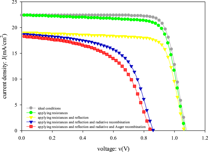
Considering all of the conditions mentioned above, the simulation was accomplished. First of all, for ideal and non-ideal conditions comparison, the simulation was performed under ideal conditions. Photovoltaic parameters for this term were obtained VOC = 1.08 V, JSC = 22.43 mA/cm2, FF = 79.63%, and PCE = 19.26%. In the following, the simulation process was performed step by step by applying each of the non-ideal conditions in each step. At the first, the Rs = 0.2 Ω.cm2, and Rsh = 900 Ω.cm2 were applied for investigating the resistances effect. The performance parameters were changed to VOC = 1.07 V, JSC = 22.43 mA/cm2, FF = 76.23%, and PCE = 18.28% values. In the next step, in addition to resistance, the reflection was applied. Its value was adjusted by 14% in the FTO contact (literature [21]). The results were acquired as VOC = 1.06 V, JSC = 19.06 mA/cm2, FF = 76.17%, and PCE = 15.43%. Radiative recombination is the dominant mechanism in perovskite solar cells due to their direct bandgap. To prove this concept, using the data in Table 2, the recombination simulation phase was accomplished in two distinct radiative and Auger steps, respectively. After exerting radiative recombination coefficients to the active layers of the solar cell, the device performance remarkably decreased. Results were obtained as VOC = 0.86 V, JSC = 18.74 mA/cm2, FF = 59.58%, and PCE = 9.62%. Applying the Auger recombination did not have considerable impact on the efficiency. However, in this step the parameters obtained as VOC = 0.84 V, JSC = 18.34 mA/cm2, FF = 54.25%, and PCE = 8.40%. Figure 1 indicates the overlapped Current-Voltage (J-V) curves of the mentioned steps.
Figure 1.
Comparison of the ideal and non-ideal conditions in the form of J-V curves.
It is observed that, as more non-ideal conditions were applied, the device performance was decreased, as well as, revealed more real performances. The outcomes are given in Table 3.
Table 3.
Photovoltaic parameters of different ideal and non-ideal conditions in step-by-step form.
| Steps | VOC (V) | JSC (mA/cm2) | FF (%) | PCE (%) |
|---|---|---|---|---|
| Ideal conditions | 1.08 | 22.43 | 79.63 | 19.26 |
| Applying resistances | 1.07 | 22.43 | 76.23 | 18.28 |
| Applying resistances + reflection | 1.06 | 19.06 | 76.17 | 15.43 |
| Applying resistances + reflection + radiative recombination | 0.86 | 18.74 | 59.58 | 9.62 |
| Applying resistances + reflection + radiative recombination + Auger recombination | 0.84 | 18.34 | 54.25 | 8.40 |
In the following sections, by considering the final step’s results, the effect of some essential layer parameters on the device performance was studied. In addition, the role of recombination plots was investigated simultaneously. The non-ideal conditions employed in this work leads to forming recombination plots. Therefore, in this study, in addition to the photovoltaic parameters of the studied cell, we considered the recombination results for selecting the appropriate parameter for the layers of the cell.
3.2. Effect of thickness
3.2.1. Effect of absorber thickness
Given the vital role of the perovskite layer in light absorption and charge generation, optimizing the perovskite layer thickness seems to be an essential task. In this research, in the range of 200–600 nm, the solar cell’s performance and recombination behavior was investigated. As mentioned earlier, it is evident that the reflection amount is affected by the thickness of the absorber. Therefore, the reflection of the solar cell in the desired thicknesses was obtained and reported in Table 4 [21].
Table 4.
The reflectance values in different thicknesses of absorber [21].
| Thickness (nm) | Reflectance (%) |
|---|---|
| 200 | 25 |
| 250 | 20 |
| 300 | 18 |
| 350 | 17 |
| 400 | 15 |
| 450 | 14 |
| 500 | 13 |
| 550 | 12.7 |
| 600 | 12.5 |
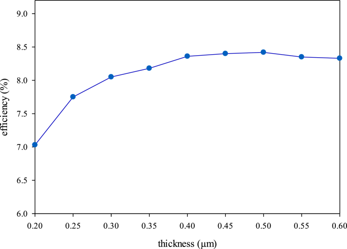
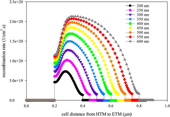
The results were represented in Figures 2 and 3 in the forms of efficiency and recombination plots as a function of the absorber thickness, respectively (The recombination paths indicated in Figure 3 were obtained using the recombination information given to the SCAPS-1D program. Moreover, the X axis is the cell distance from HTM thickness to absorber thickness and ETM thickness). As shown in Figure 2, as the thickness of the adsorbent layer increases, the efficiency also increases. This can be justified according to the perovskite layer’s absorption spectra and charge generation as described in the literature [16]. Regarding this analysis, as the absorber thickness increases, the absorption will be performed in a vast band gap and wavelength spectra. Hence, the amount of charge generation will increase. Nevertheless, after a saturation thickness, the absorption will not be performed in the vaster bandgaps. Therefore, the efficiency will not increase after this thickness. In the present work, the curves demonstrate that the cell’s efficiency results in better values in the 400 nm–600 nm range (Figure 2). However, the efficiency does not differ significantly in the selected range. Besides, variation of other photovoltaic parameters by thickness increment was represented in Figure S1.
Figure 2.
Variation of device efficiency vs. the absorber thickness.
Figure 3.
Recombination rate of different absorber thicknesses against the cell’s distance from HTM to ETM layer.
According to the results, as the absorber thickness increase, a decline is observed in the Fill Factor (FF) and Open-Circuit Voltage (VOC) diagrams due to the series resistance and recombination enhancement, respectively. Moreover, as the Short-Circuit current (JSC) refers to the charge generation, a slight increment is observed in the JSC plot by the thickness enhancement [16]. The recombination rate increases as the absorber thickness enhance (Figure 3). When the excitons (electron-hole) generation enhances, their collision probability increases. This leads to more dissipation, and therefore, recombination probability increases.
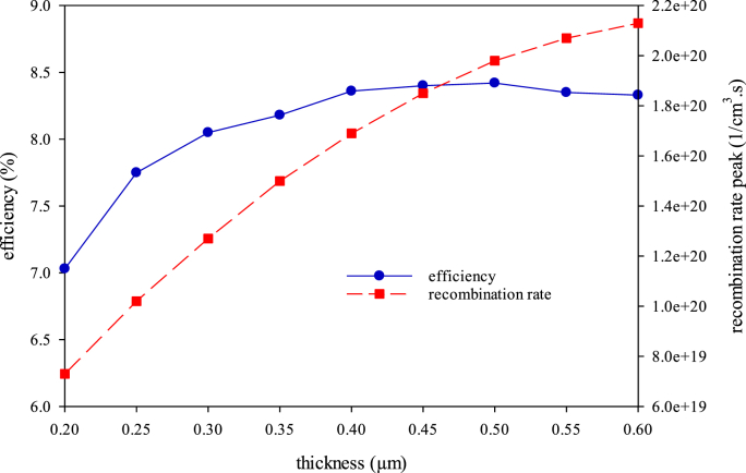
Generally, it is better to optimize the thickness using recombination and efficiency plots simultaneously. This can be possible by drawing a triaxial diagram, including the device efficiency and the recombination plot’s peaks against the thickness of absorber. This plot is given in Figure 4. It helps a better understanding of selecting the optimum thickness. In addition to the plots represented in Figures 2 and 3, from Figure 4, it can be understood that the thickness of 400 nm is the optimal choice for the absorber’s thickness due to its relatively higher efficiency and lower recombination peak.
Figure 4.
Triaxial plotting of PCE and recombination rate peaks against absorber thickness.
Since the triaxial diagrams show a more understandable scheme of selecting the appropriate parameter (such as layers thickness and doping density), in the following investigations, only this type of diagram will be presented. However, the single diagrams for the ETM and HTM layers thickness effect were given in Figures S2 and S3 (supplementary data).
3.2.2. Effect of ETM thickness
According to the perovskite’s light absorption, the electron transporting material in planar n-i-p structures must be a transparent layer. Moreover, for faster light absorption, its thickness is better to have lower values. High ETM thickness leads to recombination increment, more series resistance to the cell, and restricted transportation of electrons to the front contact [39]. In this section, considering the absorber thickness’s optimized amount, the effect of ETM thickness was investigated in the range of 40–200 nm. According to literature [21], the reflectance in the mentioned thickness range approximately possesses a constant amount equal to 15% [15]. The obtained results were illustrated in Figure 5 in terms of efficiency and recombination plots. According to the results represented in Figure 5, as the ETM thickness of the cell enhances, the efficiency generally decreases.
Figure 5.
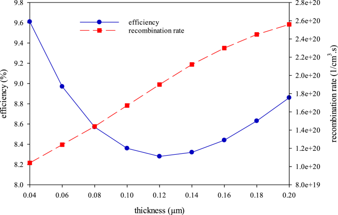
Triaxial plotting of PCE and recombination rate peaks against ETM’s thickness.
Furthermore, Figure S4 represents the variation of photovoltaic parameters by the ETM thickness enhancement. It can be concluded that, according to the higher recombination in higher ETM thicknesses, as well as late light absorption by the absorber layer, all of the cell’s photovoltaic parameters experience a decline in their value [39]. Regarding the remarkably better efficiency and less recombination, it is evident that the thickness of 40 nm with the PCE = 9.61% can be the optimal choice for ETM. It should be noted that after 120 nm, an increase has occurred in the efficiency. In an ETM layer’s thickness variation, several factors can have impact on its performance. For instance, in higher thicknesses, the charge recombination is more, but on the other side, the charge transportation can occur rapidly because of the thicker transporting layer. These mentioned factors may be dominant together in different thicknesses. As it can be seen from Figure 5, after 120 nm thickness, the charge transporting factor is dominant to the less charge recombination.
3.2.3. Effect of HTM thickness
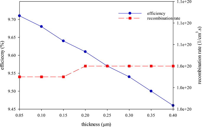
Similar to the previous sections, the HTM’s thickness variation can impact the cell’s performance, including its efficiency and recombination rate. The overlapped results of Figure 6 confirm this concept, which was investigated in the range of 50–400 nm for the HTM’s thickness and with the previous sections' optimized results. From the curves represented in Figure 6, it is evident that the performance factors containing the cell efficiency and recombination do not vary significantly as it resulted in literature [16]. Moreover, the effect of HTM thickness on the cell’s photovoltaic parameters is illustrated in Figure S5. According to the literature, after a certain HTM thickness, the cell’s parameters do not vary remarkably [16]. The HTM layer does not need to be a transparent layer as well as ETM. Hence, except for the recombination factor, the HTM’s thickness will not affect the other factors. However, due to the PCE and recombination diagrams' behavior, the optimum HTM thickness is suggested as 50 nm, revealing an efficiency of 9.71%.
Figure 6.
Triaxial plotting of PCE and recombination rate peaks against HTM’s thickness.
3.3. Effect of doping density
The doping density is an essential property of solar cells' various layers that customize their p-type or n-type form. Variations of this parameter would have different impacts and behaviors on the cell’s performance. In the following sections, the effect of this parameter in the different layers was studied.
3.3.1. Effect of absorber’s doping density
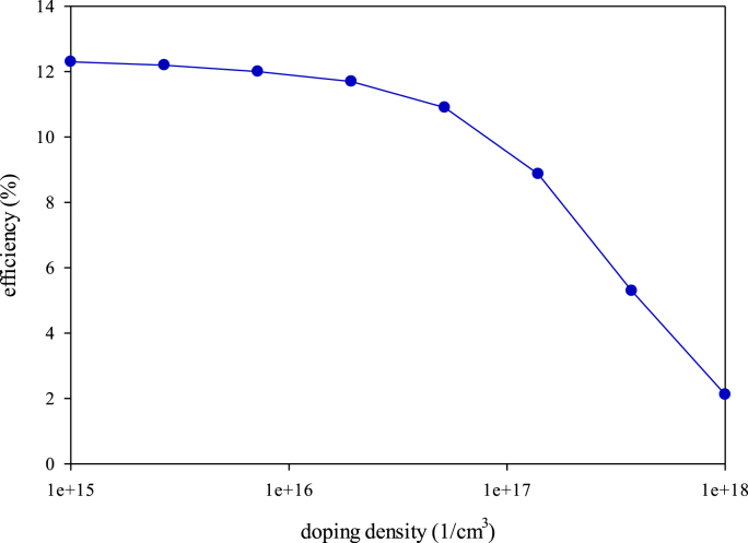
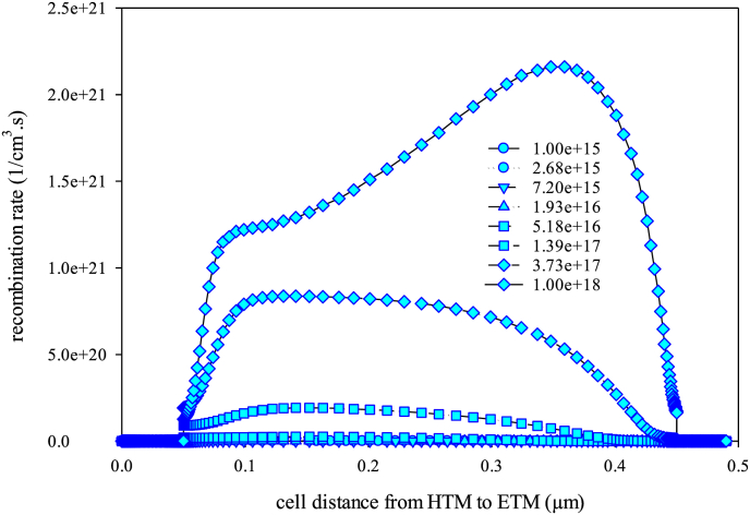
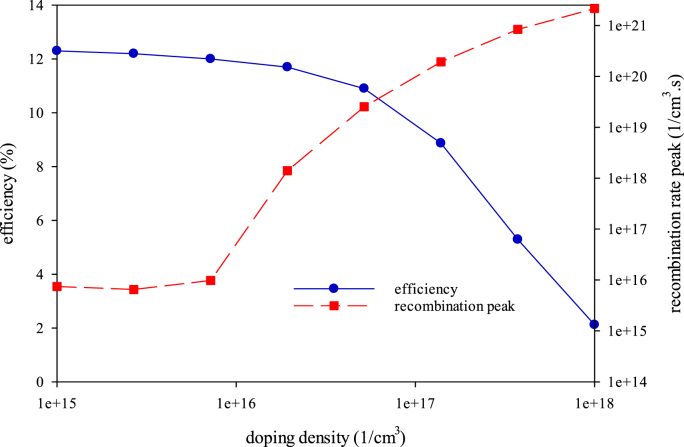
Similar to the layers' thicknesses investigation, doping density would affect recombination and power conversion efficiency plots, too. In the first step, absorber’s doping density was studied. For this purpose, in the range of 1015–1018 1/cm3, with the optimized thicknesses, the performance plots were obtained. Figures 7 and 8 demonstrate PCE and recombination rate variation as a function of the doping density and the solar cell’s thickness, respectively.
Figure 7.
Variation of device efficiency vs. the absorber doping density.
Figure 8.
Recombination rate of different densities of absorber against the cell’s distance from HTM to ETM layer.
Both diagrams represent the strictly descending behavior. It can be due to the increased chance of charge recombination by enhancing the doping density. Other photovoltaic parameters behavior represented in Figure S6 confirms this subject, too. Hence, it is evident that the amount of 1015 1/cm3 would be the most suitable value for the absorber’s doping density which produces 12.28% efficiency. For better understanding, the triaxial plot of doping density impact was given in Figure 9.
Figure 9.
Triaxial plotting of PCE and recombination rate peaks against absorber’s density.
3.3.2. Effect of ETM’s doping density
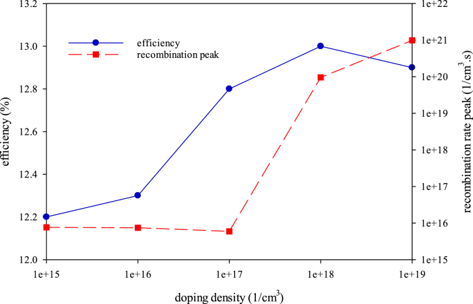
In contrast to the procedure developed in the last section for representing the doping density effect in two separate plots, in this part, with all the optimized values of the parameters mentioned above, a triaxial diagram was depicted, similar to the thickness investigation parts (single recombination rate diagrams for ETM and HTM doping density behavior is represented in Figures S7 and S8). Figure 10 reveals the mentioned results. According to the results of Figure 10, as the ETM doping density increases, the efficiency of the cell increases. We can attribute it to the ETM’s more negativity and electron transporting behavior in high doping densities. This also affects similarly the Fill Factor behavior represented in Figure S9. Moreover, according to the diagrams in Figure S9, VOC and JSC curves do not vary significantly in the selected doping density range. However, it also leads to more recombination. Therefore, unlike previous routine decisions for selecting the optimum parameter, in this section, due to the higher recombination in the higher efficiencies, some discussions around the optimum property selection should occur. As shown in Figure 10, after the donor density of 1017 1/cm3 with logarithmic increment, the efficiencies possess remarkably higher values. The efficiencies do not change much in doping densities of 1017, 1018, and 1019 1/cm3. However, the recombination rate peaks differ significantly in those values. Therefore, regarding the lower recombination in the density of 1017 1/cm3, this amount seems to be the optimum value for the ETM layer’s density. This value’s corresponding PCE was 12.79%.
Figure 10.
Triaxial plotting of PCE and recombination rate peaks against ETM’s density.
3.3.3. Effect of HTM’s doping density
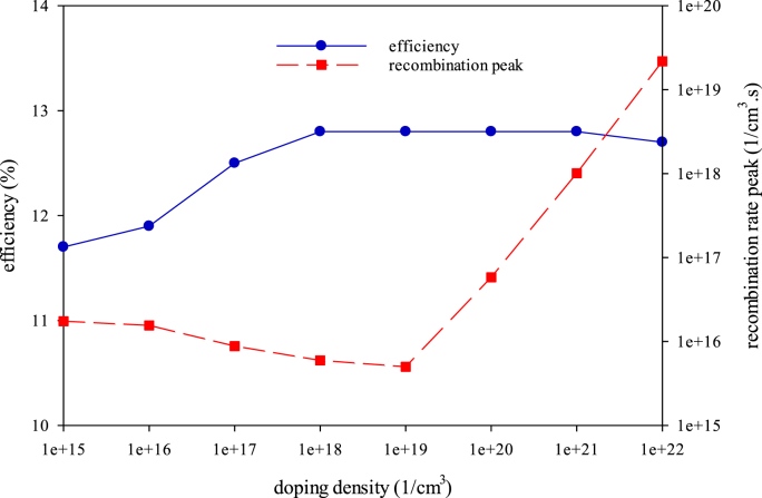
Similar to the discussion in optimizing the ETM’s doping density, in this section, the impact of HTM density’s variation in the range of 1015–1022 1/cm3 (logarithmic increment) was studied. Like the previous sections, the results were depicted in triaxial form. They are represented in Figure 11. As shown in Figure 11, regarding the high positivity and hole transporting behavior in high doping densities of HTM layer, the efficiency increases by doping density enhancement. Although, high charge density leads to high probability of excitons' generation and accordingly high recombination chance. However, from the plots of Figure 11, it is evident that in the range of 1018–1021 1/cm3, the efficiency possesses the maximum value and remains constant. Moreover, we can see similar effects on the FF plot represented in Figure S10. VOC and JSC curves remain constant by the HTM doping density variation. Similar to the ETM’s curves, the recombination rate picks differ in these densities. Therefore, recombination plays a crucial role in selecting the optimum density. Among the chosen densities, regarding the recombination variation, it seems that 1019 1/cm3 doping density with PCE = 12.83% presents the best performance.
Figure 11.
Triaxial plotting of PCE and recombination rate peaks against ETM’s density.
3.4. Final J-V curve
According to the obtained results, generally, we can declaim that despite non-ideal conditions relatively lower efficiencies, they represent a more realistic perspective of solar cells. Besides, their results are closer to the experimental research. In addition, the formation of recombination diagrams can help to decide the optimal value for the layer parameters.
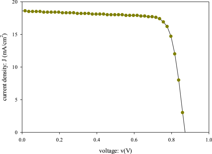
After applying all of the mentioned parameters, the final J-V curve was obtained and represented in Figure 12. By the comparison of Figures 1 and 12 diagrams, it can be observed that the area under the graph surface of Figure 12 was increased relative to the final step’s diagram in Figure 1. In the other words, in addition to area increment, the graph was become closer to the normal I–V graphs. This represents the positive effect of parameters optimization in a solar cell’s performance. For more comparison, all of the applied optimum parameter’s effects were represented in Table 5.
Figure 12.
J-V curve of the perovskite solar cell studied in this work, after applying all of the non-ideal conditions and optimum values.
Table 5.
Comparison of applied optimized parameters in the form of photovoltaic parameters.
| Steps | VOC (V) | JSC (mA/cm2) | FF (%) | PCE (%) |
|---|---|---|---|---|
| Applying resistances + reflection + radiative recombination + Auger recombination | 0.84 | 18.34 | 54.25 | 8.40 |
| Applying the optimum absorber thickness | 0.85 | 17.85 | 55.30 | 8.36 |
| Applying the optimum ETM thickness | 0.85 | 18.21 | 62.03 | 9.61 |
| Applying the optimum HTM thickness | 0.85 | 18.22 | 62.67 | 9.71 |
| Applying the optimum absorber doping density | 0.87 | 18.60 | 75.97 | 12.28 |
| Applying the optimum ETM doping density | 0.87 | 18.58 | 78.89 | 12.79 |
| Applying the optimum HTM doping density (Final step) | 0.87 | 18.58 | 79.15 | 12.83 |
| Experimental [40] | 0.974 | 23.01 | 0.56 | 12.72 |
The obtained simulation results agreed with the literature [40]. Moreover, the results of Table 6, which were collected for comparison confirm the present work’s agreement with other PSC structures. Generally, this proximity of the present work’s simulation results and reported experimental results in literature confirms the approximate accuracy of this research [5, 7, 8, 9, 40].
Table 6.
Comparison of photovoltaic parameters of recent literature in both simulation and experimental phases.
| PSC structure | VOC (V) |
JSC (mA/cm2) |
FF (%) |
PCE (%) |
Ref. | ||||
|---|---|---|---|---|---|---|---|---|---|
| Exp. | Sim. | Exp. | Sim. | Exp. | Sim. | Exp. | Sim. | ||
| FTO/SnO2/Formamidinium-based perovskite/Spiro-OMeTAD/Au | 1.00 | 1.3 | 22.6 | 20.2 | 64.4 | 72.0 | 15.1 | 18.7 | [5] |
| FTO/TiO2/Perovskite/Spiro-OMeTAD/Au | 0.96 | 0.98 | 20.62 | 20.38 | 66.41 | 66.70 | 13.15 | 13.32 | [7] |
| FTO/CdS/CH3NH3PbI3-based Perovskite/Spiro-OMeTAD/Au | 0.97 | 1.37 | 16.11 | 24.35 | 65.0 | 71.29 | 10.1 | 23.83 | [8] |
| FTO/TiO2/CH3NH3PbI3-based Perovskite/CsSnI3/Carbon | 0.99 | 1.07 | 21.55 | 21.7 | 70.83 | 79.14 | 15.21 | 18.29 | [9] |
4. Conclusion
In summary, the present work attempts to open a new perspective on the simulation of perovskite solar cells using non-ideal conditions in the SCAPS-1D simulation tool. In this study, the conventional FTO/TiO2/CH3NH3PbI3/Spiro-OMeTAD/Au structure was investigated. In the first section, by applying series and shunt resistances, reflection, and recombination coefficients, the effect of each one was studied step-by-step. After considering all of the nonidealities, the cell’s performance decreased from 19.26% in ideal conditions to 8.40% in non-ideal conditions. Next, the cell with non-ideal conditions was improved by optimizing the perovskite solar cell’s active layers' parameters containing their thickness and doping density. The optimized thickness of 400 nm, 40 nm, and 50 nm was obtained for absorber, ETM, and HTM layers, respectively. Moreover, the doping densities revealed the optimum results in 1015, 1017, and 1019 1/cm3 for absorber, ETM, and HTM layers, respectively. By applying these values, the final solar cell efficiency was achieved at 12.83%, which is in good agreement with experimental results.
Generally, the results of this study emphasize on the importance of nonidealities. Although the final results represent remarkably lower performances, but they are closer to the experimental data. Using nonidealities in future solar cell simulation studies can help researchers to validate experimental data with simulation results and vice versa.
Declarations
Author contribution statement
Seyyed Reza Hosseini: conceived and designed the experiments; performed the experiments; analyzed and interpreted the data; contributed reagents, materials, analysis tools or data; wrote the paper
Mahsa Bahramgour, Pariya Yardani Sefidi: performed the experiments; analyzed and interpreted the data; contributed reagents, materials, analysis tools or data; wrote the paper;
Asghar Moradi: conceived and designed the experiments; analyzed and interpreted the data; contributed reagents, materials, analysis tools or data;
Nagihan DELIBAS, Mir Ghasem Hosseini, Aligholi Niaei: analyzed and interpreted the data; contributed reagents, materials, analysis tools or data;
Alireza Tabatabaei Mashayekh: analyzed and interpreted the data; contributed reagents, materials, analysis tools or data; wrote the paper;
Funding statement
This research did not receive any specific grant from funding agencies in the public, commercial, or not-for-profit sectors.
Data availability statement
Data included in article/supp. material/referenced in article.
Declaration of interest’s statement
The authors declare no conflict of interest.
Additional information
No additional information is available for this paper.
Acknowledgements
The authors would like to thank the cooperation of the University of Tabriz (Iran), the University of Sakarya, and TUBITAK (Turkey).
Appendix A. Supplementary data
The following is the supplementary data related to this article:
References
- 1.Nguyen D.C., et al. Hole-extraction layer dependence of defect formation and operation of planar CH3NH3PbI3 perovskite solar cells. Phys. Status Solidi Rapid Res. Lett. 2017;11(2) [Google Scholar]
- 2.Wang T., Wang P., Ding K., Liang Q. Numerical simulation of carrier transporting layer free planar perovskite cells. Optik. 2019;179:1019–1026. [Google Scholar]
- 3.Calado P., et al. Identifying dominant recombination mechanisms in perovskite solar cells by measuring the transient ideality factor. Phys. Rev. Appl. 2019;11(4) [Google Scholar]
- 4.Liu Y., Feng K., Hsieh R.-H., Mo X. CH3NH3PbIxCl(3-x) thin film prepared by vapor transfer method for pervoskite solar cells. Mater. Lett. 2019;239:163–166. [Google Scholar]
- 5.Karthick S., Velumani S., Bouclé J. Experimental and SCAPS simulated formamidinium perovskite solar cells: a comparison of device performance. Sol. Energy. 2020;205:349–357. [Google Scholar]
- 6.Teimouri R., et al. Synthesizing Li doped TiO2 electron transport layers for highly efficient planar perovskite solar cell. Superlattice. Microst. 2020;145 [Google Scholar]
- 7.De Los Santos I.M., et al. Optimization of CH3NH3PbI3 perovskite solar cells: a theoretical and experimental study. Sol. Energy. 2020;199:198–205. [Google Scholar]
- 8.Devi N., Parrey K.A., Aziz A., Datta S. Numerical simulations of perovskite thin-film solar cells using a CdS hole blocking layer. J. Vac. Sci. Technol. B, Nanotechnol. Microelectron.: Mater., Process., Measur., Phenom. 2018;36(4) [Google Scholar]
- 9.Duan Q., et al. Design of hole-transport-material free CH3NH3PbI3/CsSnI3 all-perovskite heterojunction efficient solar cells by device simulation. Sol. Energy. 2020;201:555–560. [Google Scholar]
- 10.Salem M.S., Shaker A., Othman M.S., Al-Bagawia A.H., Fedawy M., Aleid G.M. Numerical analysis and design of high performance HTL-free antimony sulfide solar cells by SCAPS-1D. Opt. Mater. 2022;123 [Google Scholar]
- 11.Singh A.K., Srivastava S., Mahapatra A., Baral J.K., Pradhan B. Performance optimization of lead free-MASnI3 based solar cell with 27% efficiency by numerical simulation. Opt. Mater. 2021;117 [Google Scholar]
- 12.Tara A., Bharti V., Sharma S., Gupta R. Device simulation of FASnI3 based perovskite solar cell with Zn (O0. 3, S0. 7) as electron transport layer using SCAPS-1D. Opt. Mater. 2021;119 [Google Scholar]
- 13.Burgelman M., Decock K., Niemegeers A., Verschraegen J., Degrave S. 2016. SCAPS Manual. [Google Scholar]
- 14.Meyer E. Extraction of saturation current and ideality factor from measuring Voc and Isc of photovoltaic modules. Int. J. Photoenergy. 2017:2017. [Google Scholar]
- 15.Diantoro M., Suprayogi T., Hidayat A., Taufiq A., Fuad A., Suryana R. Shockley’s equation fit analyses for solar cell parameters from IV curves. Int. J. Photoenergy. 2018;2018 [Google Scholar]
- 16.Bag A., Radhakrishnan R., Nekovei R., Jeyakumar R. Effect of absorber layer, hole transport layer thicknesses, and its doping density on the performance of perovskite solar cells by device simulation. Sol. Energy. 2020;196:177–182. [Google Scholar]
- 17.Servaites J.D., Yeganeh S., Marks T.J., Ratner M.A. Efficiency enhancement in organic photovoltaic cells: consequences of optimizing series resistance. Adv. Funct. Mater. 2010;20(1):97–104. [Google Scholar]
- 18.Koide N., Islam A., Chiba Y., Han L. Improvement of efficiency of dye-sensitized solar cells based on analysis of equivalent circuit. J. Photochem. Photobiol. A: Chem. 2006;182(3):296–305. [Google Scholar]
- 19.Taghavi M.J., Houshmand M., Zandi M.H., Gorji N.E. Modeling of optical losses in perovskite solar cells. Superlattice. Microst. 2016;97:424–428. [Google Scholar]
- 20.Gorji N.E., Sohrabpoor H. Modeling of light interference in CH3NH3PbI3Clx and MAPbI3Cl perovskite solar cells. Mater. Lett. 2016;177:143–147. [Google Scholar]
- 21.Bernal-Correa R., Morales-Acevedo A. Spectral reflectance optimization for planar perovskite solar cells. Optik. 2021;227 [Google Scholar]
- 22.Luo D., Su R., Zhang W., Gong Q., Zhu R. Minimizing non-radiative recombination losses in perovskite solar cells. Nat. Rev. Mater. 2020;5(1):44–60. [Google Scholar]
- 23.Reinders A., Verlinden P., Van Sark W., Freundlich A. John Wiley & Sons; 2017. Photovoltaic Solar Energy: from Fundamentals to Applications. [Google Scholar]
- 24.Raoui Y., Ez-Zahraouy H., Tahiri N., El Bounagui O., Ahmad S., Kazim S. Performance analysis of MAPbI3 based perovskite solar cells employing diverse charge selective contacts: simulation study. Sol. Energy. 2019;193:948–955. [Google Scholar]
- 25.Abdelaziz S., Zekry A., Shaker A., Abouelatta M. Investigating the performance of formamidinium tin-based perovskite solar cell by SCAPS device simulation. Opt. Mater. 2020;101 [Google Scholar]
- 26.Khac D.L., et al. Influence/effect of deep-level defect of absorber layer and n/i interface on the performance of antimony triselenide solar cells by numerical simulation. Sustainability. 2022;14(11):6780. [Google Scholar]
- 27.Jamal M., et al. Comparative studies on the morphological, structural and optical properties of NiO thin films grown by vacuum and non-vacuum deposition techniques. Mater. Res. Express. 2021;8(12) [Google Scholar]
- 28.Burgelman A.N.-M. IEEE; New York: 1996. Presented at the Proc. 25nd IEEE Photovoltaic Spec, Washington DC. [Google Scholar]
- 29.Burgelman M., Nollet P., Degrave S. Modelling polycrystalline semiconductor solar cells. Thin Solid Films. 2000;361:527–532. [Google Scholar]
- 30.Karimi E., Ghorashi S. Investigation of the influence of different hole-transporting materials on the performance of perovskite solar cells. Optik. 2017;130:650–658. [Google Scholar]
- 31.Karimi E., Ghorashi S.M.B. Simulation of perovskite solar cell with P 3 HT hole-transporting materials. J. Nanophotonics. 2017;11(3) [Google Scholar]
- 32.Bhattacharya P. Prentice-Hall, Inc.; 1997. Semiconductor Optoelectronic Devices. [Google Scholar]
- 33.Blood P., Orton J.W. The electrical characterization of semiconductors: majority carriers and electron states. Tech. Phys. 1992;14:i–xxiii. [Google Scholar]
- 34.Hall R.N. Electron-hole recombination in germanium. Phys. Rev. 1952;87(2):387. [Google Scholar]
- 35.Mitonneau A., Mircea A., Martin G., Pons D. Electron and hole capture cross-sections at deep centers in gallium arsenide. Rev. Phys. Appl. 1979;14(10):853–861. [Google Scholar]
- 36.Nelson J. Imperial College Press; 2003. The Physics of Solar Cells. [Google Scholar]
- 37.Shockley W., Read W., Jr. Statistics of the recombinations of holes and electrons. Phys. Rev. 1952;87(5):835. [Google Scholar]
- 38.Zandi S., Razaghi M. Finite element simulation of perovskite solar cell: a study on efficiency improvement based on structural and material modification. Sol. Energy. 2019;179:298–306. [Google Scholar]
- 39.Jeyakumar R., Bag A., Nekovei R., Radhakrishnan R. Influence of electron transport layer (TiO2) thickness and its doping density on the performance of CH3NH3PbI3-based planar perovskite solar cells. J. Electron. Mater. 2020;49(6):3533–3539. [Google Scholar]
- 40.Visoko U., Son I.P., Celice N. High-efficiency perovskite solar cells improved with low-cost orthorhombic Cu2Znsns4 as the hole-transporting layer. Mater. Tehnol. 2018;52(4):483–486. [Google Scholar]
Associated Data
This section collects any data citations, data availability statements, or supplementary materials included in this article.
Supplementary Materials
Data Availability Statement
Data included in article/supp. material/referenced in article.


