

Abstract
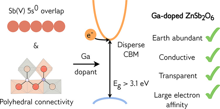
Transparent conducting oxides have become ubiquitous in modern optoelectronics. However, the number of oxides that are transparent to visible light and have the metallic-like conductivity necessary for applications is limited to a handful of systems that have been known for the past 40 years. In this work, we use hybrid density functional theory and defect chemistry analysis to demonstrate that tri-rutile zinc antimonate, ZnSb2O6, is an ideal transparent conducting oxide and to identify gallium as the optimal dopant to yield high conductivity and transparency. To validate our computational predictions, we have synthesized both powder samples and single crystals of Ga-doped ZnSb2O6 which conclusively show behavior consistent with a degenerate transparent conducting oxide. This study demonstrates the possibility of a family of Sb(V)-containing oxides for transparent conducting oxide and power electronics applications.
Transparent conducting oxides (TCOs) are an essential component of modern photovoltaic and display screen technologies. Thin-film Sn-doped In2O3 (ITO) displays the superior optoelectronic properties among the industrially used TCOs; it has been reported to possess resistivities as low as 8 × 10⁻⁵ Ω·cm, mobilities that exceed 50 cm2 V–1 s–1, and carrier concentrations on the order of 1 × 1021 cm–3, all while retaining over 90% transparency to visible light.1 The more earth-abundant TCOs, such as F-doped SnO2 (FTO)2 or Al-doped ZnO (AZO),3 display mobilities and conductivities below those of ITO, which limits their application in display screen technologies. However, it is undesirable to continue to use ITO for large-area applications such as in photovoltaics, despite recent improvements in the efficiency of indium-based TCOs via innovative doping (Mo and Ce),4−6 due to the expense and scarcity of indium. Therefore, there is a drive to try to increase the performance of the known earth-abundant TCOs7,8 or, more unusually, to discover new TCOs. The last “new” materials demonstrated to be TCOs were the thin-film correlated metals SrVO3 and CaVO3 in 2015 and single-crystal La-doped BaSnO3 in 2012.9,10
In terms of materials design, the common trend in the majority of the effective n-type TCOs is the presence of post-transition-metal cations with the electronic structure (n – 1)d10ns0np0. In these materials, the valence s orbitals of the cation hybridize with antibonding oxygen 2p states, yielding conduction bands with low electron effective masses.11 Indeed, the majority of the cations in the industrially relevant TCOs are limited to groups 12, 13, and 14 of the periodic table.
In an early investigation of ternary oxides, Shannon et al. noted that edge-sharing Cd2+, In3+, and Sn4+ octahedra were a feature of common transparent conductors.12 Mizoguchi and Woodward built on this in 2004, investigating the necessity for edge-sharing octahedral connectivity when designing n-type TCOs.13 They found that edge-sharing is not a prerequisite, and corner-sharing can also provide excellent dispersion of the conduction band, such as in BaSnO3.10 Interestingly, they identified some ternary oxides containing Sb(V) and Bi(V) which displayed reasonable curvature of the conduction band minimum (CBM),13 including tri-rutile zinc antimonate, ZnSb2O6. It should be noted that group 15 cations in their highest oxidation states possess the same (n – 1)d10ns0np0 electronic structure as the cations in the common, successful TCOs.
In 2014, a computational screening study from Hautier et al. also proposed ZnSb2O6 as a potential transparent conductor, in particular noting its low electron effective mass and earth-abundant, nontoxic composition.14 Several other stibnates and germanates were highlighted, but none was followed up with a defect chemistry analysis showing n-type dopability. On the few occasions that ZnSb2O6 has been synthesized experimentally, transparent conducting behavior has not been observed. Kikuchi et al. investigated it as a TCO and thermoelectric in 2005,15 but it was only produced as a powder, and little data on the optoelectronic properties were published. Thick films of crystalline ZnSb2O6 have been deposited for gas-sensing applications via dip-coating and vapor-phase oxidation methods,16,17 although no assessment of their transparent conducting potential has been reported. Spin-coating of a nanoparticle precursor followed by high-temperature annealing was found to result in transparent insulating ZnSb2O6 thin films, which deteriorated in terms of both transparency and crystallinity upon F-doping.18 Finally, Li et al. briefly investigated ZnSb2O6 as a potential anode for Li battery technology.19 Synthesis of high-quality thin films or single crystals of ZnSb2O6 has not been realized, and its full potential as a transparent conductor has yet to be assessed.
In this work, we investigated the crystal and electronic structure of ZnSb2O6 with hybrid density functional theory, and validated this description with quasi-particle self-consistent GW theory (Green’s function, G, with a screened Coulomb interaction, W). A full intrinsic defect analysis was performed that showed that, when nominally undoped, ZnSb2O6 does not fulfill the Mott criterion for metallic-like conductivity. We then considered three extrinsic dopants, and demonstrated that Ga is the optimum electron donor in ZnSb2O6. Using this knowledge, we successfully grew powder and single-crystal samples of Ga-doped ZnSb2O6, which displayed a low absorption coefficient (88 cm–1) in the visible range, electron mobility up to 49 cm2 V–1 s–1, conductivity up to 1890 S cm–1, carrier concentrations on the order of 2 × 1020 cm–3, and a Haacke figure of merit comparable with that of polycrystalline ITO. We calculated the electron affinity of ZnSb2O6 to be nearly 1 eV larger than that of currently available transparent electrodes, offering much needed diversity when considering the band alignment of potential contact layers in devices. Ga-doped ZnSb2O6 displays all the indicators of a high-performance transparent conductor, with the added bonus of being comprised of earth-abundant elements: Zn and Sb are several orders of magnitude cheaper per kilogram than In, while Ga is required in only very small amounts.20 This study stands as an important proof-of-concept for Sb(V)-based TCO design, and invites the development of thin-film deposition to further investigate the optoelectronic properties of ZnSb2O6 and to prepare it for use in devices and commercial applications.
Crystal Structure
ZnSb2O6 crystallizes in a tri-rutile structure, belonging to the P42/mnm space group, as shown in Figure 1a. The structure consists of ZnO6 and SbO6 edge-sharing octahedra in the order ZnO6–SbO6–SbO6 along the c-axis, with corner-sharing octahedra present throughout the a–b planes (Figure 1a,b). The unit cell is tetragonal, and a summary of the fundamental parameters is provided in Table S1 for a range of exchange correlation functionals and experiments. The powder X-ray diffraction (XRD) results show an excellent fit to the P42/mnm space group, as can be seen in Figure 1c, and the calculated PBE0 lattice parameters are in good agreement with room-temperature XRD results. We note the PBEsol lattice parameters are slightly overestimated, which is typical of the generalized gradient approximation (GGA) implementation in DFT.21
Figure 1.

(a) View along the a-axis of the crystal structure of ZnSb2O6. (b) Octahedral connectivity in ZnSb2O6, viewed from a slight offset of the a-axis, which is edge-sharing in the c-direction and corner-sharing in the a- and b-directions. (c) Powder and simulated X-ray diffraction patterns for ZnSb2O6. The dashed line indicates Rietveld refinement for P42/mnm tri-rutile structure; the difference between fit and data is shown below the peak positions. The inset shows the typical shift in an XRD peak upon Ga-doping. (d) Undoped ZnSb2O6 single crystals and (e) Ga-doped ZnSb2O6 single crystals. All crystal structures were visualized using VESTA.22
Doping with Ga causes a systematic shift in the Bragg peaks to higher angles compared to those of undoped samples, illustrated in the inset of Figure 1c, indicating a shrinkage in cell size. This observation is consistent with substituting Ga with Zn in an octahedral environment, as Ga has a smaller ionic radius (0.62 Å) compared to Zn (0.74 Å).23 The unit cell volumes shift from 201.78 Å3 to 201.48 Å3 after 6% Ga doping, extracted by Rietveld refinement using the GSAS-II software.24 These observations are consistent with a solid solution of gallium replacing zinc in the tri-rutile structure, with no detectable phase separation. Optical images of our transparent undoped and Ga-doped single crystals are shown in Figure 1d,e, approximately 1 mm2 in area and polished to a thickness of around 150 μm.
Electronic Structure
We begin with a discussion of the electronic structure, arguably the most decisive indicator of a prospective transparent conductor. The electronic band structure of ZnSb2O6 was calculated using the PBE0 functional and is displayed in Figure 2a. A direct band gap of 3.54 eV at Γ is observed, with relatively high dispersion at the CBM. The electron effective mass in the Γ→X and Γ→M directions is 0.27me, and improves further along Γ→Z (in the c-direction) to 0.22me. The high dispersion originates from the broad overlap of Sb 5s orbitals, which are the main contributors to the CBM density of states, with Zn and O s states. Qualitatively, the conduction band shape is in good agreement with previous GGA-DFT calculations, while the hybrid functional corrects for the systematic underestimation of the band gap,14 which we note is competitive with state-of-the-art TCOs In2O3, SnO2, ZnO, and BaSnO3.2,7,8,25Figure S6 shows the band structure computed with hQSGW theory, which shows a small (3%) decrease in the direct band gap to 3.41 eV, with the electron effective masses unchanged. Ultimately, the PBE0 description is sufficient, accurately describing the nature of the band gap compared to the next level of theory, and is used subsequently for defect calculations. The transition from valence band maximum (VBM) to CBM is symmetry forbidden, and the first allowed transition occurs from states around 0.7 eV below the VBM (similar to the case in In2O3),26 as denoted by the green arrow in Figure 2a. This is discussed in greater detail in the Optical Properties section.
Figure 2.

(a) Electronic band structure of ZnSb2O6 computed using the PBE0 functional. (b) Simulated valence band spectra using the PBE0 functional, weighted by the photoionization cross sections for a photon energy of 5.91 keV, and broadened by a Gaussian of 0.6 eV and a Lorentzian of 0.2 eV. Plotted in black is the HAXPES experimental valence band spectrum of a nominally undoped single crystal, collected at a photon energy of 5.91 keV. Both spectra are normalized to the peak maxima.
Simulated and experimental photoelectron spectra of the valence band of undoped ZnSb2O6 are shown in Figure 2b, plotted using Galore.27,28 The simulated spectrum was obtained from the PBE0 density-of-states calculation, where the orbital contributions were weighted with tabulated photoionization cross sections and broadened with Guassian and Lorentzian functions to reproduce the experimental line shapes. The spectra were approximately aligned to the Fermi level. The key valence band features in Figure 2b are in agreement: an initial onset mainly comprised of Zn 3d, Sb 4d, and O 2p states followed by a sharp peak assigned to Zn 3d states. However, the position of this peak is under-bound by approximately 3 eV. The under-binding of transition metal d states with hybrid DFT is well documented and has been observed in other well-known TCOs, such as the Zn 3d states in ZnO and Sn 4d states in SnO2.29,30
Defect Chemistry
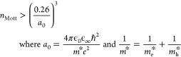
While the electronic structure of ZnSb2O6 is a promising indicator of high TCO performance, it is the defect chemistry that will ultimately control the electrical properties of the system. Degenerate conductivity is achieved when the charge carrier concentration exceeds the Mott criterion:32−35
 |
1 |
which for ZnSb2O6 is 2.6 × 1018 cm–3, where a0 is the effective Bohr radius (1.89 × 10⁻⁹ m), ϵ0 is the calculated static dielectric constant (7.74), and m* is the reduced effective mass (1.97 × 10⁻³¹ kg).
We first identify the thermodynamic stability region (blue) of ZnSb2O6 with respect to its competing phases in Figure 3a. This gives an insight into which synthesis conditions are most appropriate for growing n-type ZnSb2O6 (denoted by the orange circle), and provides the chemical potentials required for calculating the defect formation energies under those synthesis conditions (equation S1). The transition level diagram for intrinsic defects, namely zinc, antimony, and oxygen vacancies (VZn, VSb, and VO), cation substitutions (ZnSb and SbZn), and various interstitial sites (Zni, Sbi, and Oi), is calculated and displayed in Figure 3b for the most n-type chemical potential limits, corresponding to an oxygen-poor, metal-rich environment.
Figure 3.

(a) Thermodynamic stability region of ZnSb2O6, calculated using CPLAP.31 The orange marker denotes the most n-type growth conditions, the chemical potential limits at which the defect formation energies in this work are reported. (b) Intrinsic defect transition level diagram of ZnSb2O6. (c) Extrinsic defect transition level diagram of ZnSb2O6. (d) Experimental HAXPES valence band spectra of undoped and Ga-doped ZnSb2O6, normalized to area under the curve. The inset shows a ×125 magnification at the Fermi level, denoted by a dotted gray line. For transition level diagrams, blue and orange shaded regions denote the valence and conduction bands, respectively. Each colored line represents a different defect, and the gradient of that line denotes the charge state. Filled circles represent transition levels, where two charge states are in thermodynamic equilibrium. Calculated and plotted using AIDE. For VO, Oi, FO, Zni, and Gai, only the lower energy of the two non-equivalent defect sites is plotted. The gray lines in (c) show the native p-type acceptor defects VZn and ZnSb.
The intrinsic defect chemistry does not support degenerate n-type behavior. VO acts as a deep donor defect, in line with the behavior observed in established TCOs such as In2O3, SnO2, and ZnO (CdO being the notable exception),5,8,36−38 and is discussed in greater detail in the SI. The SbZn substitution is the next lowest energy species, but it is charge-compensated by VZn (see Figure S5) just below the CBM, pinning the Fermi level in the gap. We predict the position of the Fermi level and charge carrier concentrations through a self-consistent Fermi level (SCFL) analysis. The synthesis temperature of our ZnSb2O6 single crystals is ∼1400 K, and by fixing the defect concentrations present at this temperature and recalculating the SCFL at room temperature, we can predict room-temperature experimental charge carrier concentrations. Undoped ZnSb2O6 is predicted to have 3.1 × 1016 cm–3 charger carriers (significantly below the Mott criterion), with the SCFL 0.13 eV below the conduction band edge, precluding undoped ZnSb2O6 from metallic-like conductivity. From experiment, we measure 5.0 × 1017 cm–3 carriers in undoped crystals, around an order of magnitude more than predicted, and low conductivity (around 2 S/cm). The slight deviation in carrier concentration measured in the crystals is likely due to adventitious H-doping during synthesis, as well as trace amounts of other impurities that could contribute electrons (such as Cl from the carrier gas), but is in qualitative agreement with the SCFL analysis—i.e., when nominally undoped, ZnSb2O6 does not display metallic conductivity.
Next, we considered a strategy for electron donation in ZnSb2O6. Knowing that the Sb s states mainly comprise the conduction pathway, we primarily targeted the Zn and O sites for substitution to leave the conduction band unperturbed. Ruling out some of the larger 3+ cations, as they would cause large lattice disruption, Al, Ga (for Zn substitution), and F (for O substitution) were selected as potential dopants for driving the Fermi level into the conduction band and realizing degenerate conductivity.
The transition level diagram for Ga-doping is shown in Figure 3c, while the Al and F data is presented in Figure S8. We find that GaZn and AlZn are low-energy donors, with formation energies of 0.45 eV and 0.58 eV in their neutral charge states, respectively. In both cases, the dopant interstitial defects are rather high in energy (around 5 eV at the CBM), and are charge-compensated by their respective dopant substitutions onto the Sb site. FO anion substitutions have higher formation energies of 1.38 eV and 1.46 eV for the inequivalent oxygen sites, while the F interstitials do not donate electrons to the conduction band. Crucially, we find that the native p-type defects, VZn and ZnSb, are too high in energy to charge-compensate GaZn, AlZn, and FO. We complete the same SCFL analysis as before for each case, and find that Ga has a predicted room-temperature charge carrier concentration of 3.4 × 1019 cm–3 and a SCFL of 3.69 eV (0.15 eV above the CBM), thereby predicting degenerate conductivity. For Al and F, the predicted charge carrier concentrations are 3.2 × 1019 cm–3 and 7.2 × 1018 cm–3, with the SCFL sitting above the CBM in both cases. However, Al-doping of ZnSb2O6 was unsuccessful experimentally, with various Al precursors not responding well to the CVT growth method, and F-doping was not attempted due to the lower predicted achievable carrier concentration, so Ga emerged as the optimal dopant. Experimentally, we record carrier concentrations of 8.9 × 1019 cm–3, 2.0 × 1020 cm–3, and 2.4 × 1020 cm–3 in three single crystals when doped with increasing Ga content. The presence of adventitious H is the most likely origin of discrepancy, but again we find qualitative agreement with the SCFL analysis. Conductivity rises with increasing carrier concentration and Ga-doping content by several orders of magnitude in the single crystals to 526 S cm–1, 1230 S cm–1, and 1890 S cm–1, respectively, and a similar trend is observed in the powders (conductivity plotted in Figures 4c, S1, and S2), competitive with established TCOs.
Figure 4.

(a) Experimental mobility of undoped and Ga-doped single-crystal ZnSb2O6. (b) Simulated (using AMSET) mobility of ZnSb2O6 at carrier concentrations measured from experiment. (c) Single-crystal and simulated conductivity over a range of carrier concentrations, with THz spectroscopy data for an 8% Zn1–xGaxSb2O6 solid solution plotted as gray stars. (d) Calculated room-temperature scattering rates at 2.4 × 1020 cm–3. Abbreviations: ADP, acoustic deformation potential scattering; IMP, ionized impurity scattering; and POP, polar optical phonon scattering. Moving from low to high carrier concentrations causes a switch in dominant scattering from POP to IMP.
Through hard X-ray photoelectron spectroscopy (HAXPES), we find further evidence to support this description of the defect chemistry of ZnSb2O6. At high photon energies (approaching 6 keV), we can exploit the greater photoionization cross-section of Sb 5s states, which from the density-of-states calculation we expect make up the CBM, allowing us to observe any filled conduction band states (more information on the HAXPES results can be found in the SI). Figure 3d shows the HAXPES valence band spectra for undoped and Ga-doped ZnSb2O6 aligned to the Fermi level of the doped sample at 0 eV binding energy, with an expanded view (×125 magnification) provided in the inset between binding energies of 0.75 eV and −0.75 eV. In the undoped sample, there is no photoemission at a binding energy of 0 eV, implying that the conduction band states are unfilled, while the doped sample shows conduction band emission with a typical Fermi–Dirac-like distribution. This is strong evidence of degenerate filling of the conduction band upon Ga-doping, supporting the prediction of metallic-like conductivity from our defect calculations.
Charge Transport Properties
Charge transport properties are important metrics in assessing the performance of prospective TCOs. Specifically, it is desirable for a TCO to possess high electron mobility in order to maximize conductivity. Figure 4a shows the experimental electron mobility of undoped and Ga-doped ZnSb2O6 single crystals over the temperature range 200 to 350 K, where we observed an impressive room-temperature mobility of 49 cm2 V–1 s–1 at the maximum doping level (2.4 × 1020 cm–3), resulting in a conductivity of 1890 S cm–1. Our THz domain spectroscopy (TDS) results on powder samples also demonstrate metallic-like conductivity, with a conductivity of 1100 S cm–1 achieved at room temperature for Zn0.92Ga0.08Sb2O6 (gray stars in Figure 4; the full THz conductivity data set is shown in Figures S1 and S2). Our single crystals display electronic properties that are competitive with those of thin films of ITO, FTO, and AZO, which typically display electron mobilities of 40 cm2 V–1 s–1 to 60 cm2 V–1 s–1 and conductivity on the order of 1 × 10⁴ S cm–1.2,5,7 In such films, mobility is often limited by ionized impurity scattering, despite the presence of grain boundaries. With suitable deposition conditions and an optimized doping level (sufficiently raising the Fermi level above the conduction band), efficient electron tunneling through grain boundaries can passivate scattering from such defects.39 Polycrystalline ZnSb2O6 films may display reduced electron mobility compared to our single crystals due to grain boundary scattering, but with an optimized deposition process this mechanism could be suppressed as in the other successful doped TCOs.
To further understand the origin of the high mobility in ZnSb2O6, we performed charge transport calculations using the AMSET package.40 This allowed us to calculate the limits to intrinsic mobility from various scattering mechanisms including polar optical phonons (POP), acoustic deformation potentials (ADP), and ionized impurities (IMP). We found that at low carrier concentrations, corresponding to the nominally undoped sample, polar optical phonon scattering dominates, while at higher concentrations the limiting scattering mechanism switches to ionized impurity scattering. This is demonstrated in Figure 4b, where the mobility of the undoped sample displays the strong temperature dependence typically associated with a system dominated by POP scattering, while at high carrier concentrations the mobility becomes largely temperature independent, indicative of IMP-based scattering. We note that in ZnSb2O6, ADP scattering is largely unimportant, remaining unchanged and at a significantly lower rate than the other mechanisms, regardless of temperature and carrier concentration. In Figure 4d, we explicitly plot the scattering rates at room temperature and high carrier concentration, clearly showing ionized impurity scattering as the dominant scattering mechanism.
There are some discrepancies between the experimental observations and simulations. First, our calculations predict that the nominally undoped material should exhibit a very high electron mobility of around 70 cm2 V–1 s–1 at room temperature and display a strong temperature dependence. However, our undoped crystal shows the lowest mobility and only a weak temperature dependence. The trend of mobility with increased carrier concentration is in fact unclear across the whole batch of samples. Possible causes of these discrepancies include non-uniform distribution of the dopant during the chemical vapor transport (CVT) growth process, other unintentional impurities in the samples (perhaps Ca, as observed in the hard X-ray survey spectrum, Figure S3a) that could have detrimental effects on the mobility, or directional dependence effects during measurement of the single crystals—the mobility of ZnSb2O6 has reasonable anisotropy, as shown in Figure S7. One other important consideration is that these crystals are very small, only 1 mm2, so there is a reasonable error in the measurement. Synthesis of larger single crystals with a refined growth technique could result in improved mobility approaching the value predicted by AMSET; a comparison between calculated and experimental mobility for 24 binary, ternary, and quaternary compounds can be found in ref (40), and is generally reflective of the maturity of the synthesis route. It is also possible that scattering mechanisms not included within the AMSET implementation, such as nonpolar optical phonon scattering, act to lower the experimental mobility and contribute to the discrepancy. Nevertheless, the qualitative agreement between theory and experiment in this study is promising and demonstrates the feasibility and realization of Ga-doped ZnSb2O6 as a transparent conducting oxide competitive with industry standard materials.
Optical Properties
Tauc analysis suggests an optical band gap for undoped ZnSb2O6 of 3.38 eV, which increases to 3.56 eV upon Ga-doping. This widening of the band gap upon Ga-doping is characteristic of the Moss–Burstein shift that is common among the degenerately doped TCOs. The Tauc-derived band gap for the undoped sample is in remarkably good agreement with the predicted fundamental gap of 3.41 eV from the hQSGW calculation.
In Figure 5a, the absorption coefficient of undoped and Ga-doped ZnSb2O6 is plotted over the visible range, along with the calculated PBE0 value. We note that the measured absorption coefficient is below 100 cm–1 in both undoped and doped samples at a wavelength of 550 nm, corresponding to the dotted gray line. Further investigation of the computed absorption spectrum revealed a much stronger (several orders of magnitude) absorption onset at around 4.2 eV, shown in Figure 5b. This suggests that the fundamental transition at Γ between the VBM and CBM is forbidden in ZnSb2O6, and that the actual optical band gap could be up to 0.7 eV larger. Experimentally, the thickness of our single crystals prevents us from probing beyond the initial photon absorption peak, causing the plateau at around 300 cm–1. It is known that if sample thickness is too large, transmission can be blocked by a relatively low absorption coefficient beyond the initial onset, as observed in GeSe. In this material, an indirect band gap of around 1.0 eV and absorption coefficient of 150 cm–1 are measured in single crystals, and transmission is prevented beyond this energy, while a direct gap of 1.3 eV can be measured in thin films.42 Our current calculations predict a large optical band gap of around 4.2 eV, but deposition of thin-film ZnSb2O6 is required to ratify the true nature and magnitude of the band gap.
Figure 5.

(a) Experimental absorption coefficient of undoped and Ga-doped single crystals, with the calculated PBE0 absorption coefficient (pink) plotted in the same range. (b) Extended plot of the calculated PBE0 absorption coefficient, revealing the much larger value of the optical band gap. (c) Experimental transmission of undoped and Ga-doped single crystals across the visible range. Dotted gray line shows 550 nm on absorption and transmission plot. (d) Haacke figure of merit data at transmittance wavelength of 550 nm, using the doped single-crystal optical data and extracted to different thicknesses, with comparison to data for polycrystalline ITO.41
The optical transparency of our 150 μm single crystals can be seen in Figure 1d,e and in the transmission intensity plot in Figure 5c. The undoped crystal is transparent and clear, while the Ga-doped crystal displays a blue tint. The corresponding transmission intensities for the single crystals at a wavelength of 550 nm are 58% and 27%, respectively, denoted by the dotted gray line. Clearly, doping has a detrimental effect on the transparency, which has also been observed in the literature when attempting to dope thin-film ZnSb2O6 with F.18 The origin of this decrease in transmission is uncertain—we do not observe any mid-gap states from HAXPES that could signify electrons trapped on defect sites in the band gap. The concentration of VO is not predicted to rise with Fermi level modulation. In contrast, the concentration of SbZn is predicted to decrease—this suggests that neither of these defects is responsible for any loss in transmission. It is possible that transitions from the filled conduction band states to the next-available empty band could cause a mild coloration, as has been investigated in other TCOs.43 Despite this, moving from a thickness of 150 μm to 150 nm by application of the Beer–Lambert law to the 550 nm transmission data for the doped crystal, the transmission is predicted to exceed 99%, suggesting that, at commercially relevant thicknesses, the optical transparency of ZnSb2O6 could in fact be superior to that of industry standard ITO.
Finally, we derive the Haacke figure of merit (FOM) for the same Ga-doped crystal, plotted in Figure 5d. This indicates an extremely high FOM at micron thicknesses (approximately 0.2 Ω–1), and values competitive with those of industry standard ITO at thicknesses approaching 100 nm. The development of thin-film ZnSb2O6 will allow a more direct comparison of both optical transmission and FOM, rather than using the predicted thin-film transmission intensities.
Band Alignment
Having verified our computational predictions through single-crystal growth and characterization, we investigated the potential of ZnSb2O6 as a transparent electrode by calculating its band alignment and comparing to those of existing TCOs, shown in Figure 6. Our calculations reveal an ionization potential (IP) and electron affinity (EA) of 9.6 and 6.1 eV, respectively. Sb 5s states contribute strongly to the CBM, much like ns states in the other post-transition metal TCOs, but sit lower in energy due to the increased distance from the nucleus and improved shielding of effective charge by core electrons. Therefore, the EA of ZnSb2O6 is significantly greater than that of the industry-leading TCOs. Upon Ga-doping, the Fermi level is predicted to sit above the CBM, which means a work function nearly 1 eV larger than that of In2O3 could be achieved. This large work function has tremendous implications in organic photovoltaics (OPVs), which rely entirely on the charge extraction capability of the positive and negative electrodes. A transparent anode with a large electron affinity allows for closer band alignment to low-lying HOMOs (highest occupied molecular orbitals) in OPV devices, providing better Ohmic contacts, an increase in output voltage, and an enhanced device efficiency.46,47 Furthermore, replacing organic hole-extracting layers like PEDOT:PSS with a metal oxide like ZnSb2O6 could help to reduce the corrosion on the electrode.48 To engineer large work functions in existing TCOs, modulation of the conduction band is required by alloying with heavy, and sometimes toxic, elements (for example, In2-xTlxO3 and Sn1-xPbxO2).37,49 Exploiting the native band alignment in ZnSb2O6 is a much cheaper, safer, and easier way of incorporating a large work function material into devices.
Figure 6.
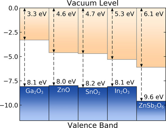
Calculated band alignment of ZnSb2O6 compared against common TCOs.37,44,45
We have used ab initio calculations to confirm that ZnSb2O6 is an earth-abundant transparent conducting oxide, which we have successfully grown in single-crystal form via chemical vapor transport. By studying the intrinsic and extrinsic defect chemistry, we were able to identify an effective doping strategy in order to realize degenerate conductivity through Ga-doping. We have used state-of-the-art packages to predict carrier concentrations and to calculate electron scattering rates, giving a more accurate prediction of charge transport properties that goes beyond the constant relaxation time approximation. Overall, we find good qualitative agreement between these predictions and our single crystals, with our best samples achieving carrier concentrations in excess of 2 × 1020 cm–3, electron mobility up to 49 cm2 V–1 s–1, and conductivity of 1890 S cm–1. The optical behavior of ZnSb2O6 is also promising, with a direct (forbidden) band gap of around 3.4 eV and a wider predicted optical gap up to 4.2 eV, although the slight blue coloration upon Ga-doping requires further investigation. The next logical step is to develop a thin-film deposition process for Ga-doped ZnSb2O6, in order to test its performance when incorporated into a device, and to better understand the relationship between charge carrier concentration, transport properties, and optical band gap. Overall, this discovery is a significant milestone in the development of earth-abundant transparent conductors, offering a high-performance alternative to industry standard materials with a unique band edge energy alignment, and opens the door to a whole family of Sb(V)-based transparent conducting oxides.
Acknowledgments
This work used the ARCHER and ARCHER2 UK National Supercomputing Service (https://www.archer2.ac.uk), via our membership of the UK’s HEC Materials Chemistry Consortium, which is funded by the EPSRC (EP/L000202, EP/R029431, and EP/T022213). We are grateful to the UK Materials and Molecular Modelling Hub for computational resources (Thomas and Young), which is partially funded by the EPSRC (EP/P020194/1 and EP/T022213/1). The authors acknowledge the use of the UCL Legion, Myriad, Kathleen, and Thomas High Performance Computing Facilities (Legion@UCL, Myriad@UCL, Kathleen@UCL, Thomas@UCL), and associated support services, in the completion of this work. We acknowledge Diamond Light Source for access to beamline I09 under proposal number SI24449-1. J.W. and D.O.S. acknowledge Diamond Light Source for co-sponsorship of an Eng.D. studentship on the EPSRC Centre for Doctoral Training in Molecular Modelling and Materials Science (EP/L015862/1). A.J.J. and D.O.S. acknowledge support for the EPSRC (grant number EP/N01572X/1). W.W.W.L. acknowledges a Royal Society of Chemistry Researcher Mobility Grant. The authors thank Gavin Stenning at the ISIS material characterization lab for use of XRD and Quantum Design PPMS. We acknowledge useful discussions with Dr. John Buckeridge and Dr. Christoper N. Savory.
Further experimental and computational data can be found at DOI: 10.5281/zenodo.7034578.
Supporting Information Available
The Supporting Information is available free of charge at https://pubs.acs.org/doi/10.1021/acsenergylett.2c01961.
THz spectroscopy, HAXPES survey and core levels, EDS spectra, an extended discussion intrinsic defects, lattice parameters, hQSGW band structure, calculated material properties used for charge transport calculations, directional dependence plots of charge carrier mobility, and Al and F transition level diagrams, including eq S1, Tables S1–S3, and Figures S1–S8 (PDF)
Author Contributions
‡ A.J.J., B.J.P., and J.W. contributed equally to this work. DFT calculations were performed by A.J.J., J.W., and A.M.G. with guidance from B.A.D.W. and D.O.S. AMSET calculations were performed by A.M.G. and analyzed by A.M.G. and J.W. Crystal growth and characterization was performed by B.J.P. L.S.I.V. assisted B.J.P. and R.P. performing charge transport measurements. Powder samples were grown and characterized by W.W.W.L. with guidance from R.G.P. and T.-C.L. and assistance from Y.L. Terahertz spectroscopy was performed by W.W.W.L. with assistance from J.N. and C.A.S. Single-crystal optical analysis was performed by T.D.V. HAXPES experiments were performed by B.J.P. and J.W. with guidance from A.R. and T.-L.L. HAXPES data analysis was performed by J.W. with assistance from A.R. T.K.K., M.H., L.S.I.V., R.K., T.-L.L., and A.R. assisted with synchrotron data collection throughout the project. The manuscript was written and prepared by J.W. with input from all authors. Crystal growth and characterization was managed by R.P. Computational work was managed by D.O.S. The overall project was conceived by D.O.S.
The authors declare no competing financial interest.
Author Status
† Deceased, July 26, 2020.
Supplementary Material
References
- Granqvist C.; Hultåker A. Transparent and conducting ITO films: new developments and applications. Thin Solid Films 2002, 411, 1–5. 10.1016/S0040-6090(02)00163-3. [DOI] [Google Scholar]
- Swallow J. E. N.; Williamson B. A. D.; Whittles T. J.; Birkett M.; Featherstone T. J.; Peng N.; Abbott A.; Farnworth M.; Cheetham K. J.; Warren P.; Scanlon D. O.; Dhanak V. R.; Veal T. D. Self-Compensation in Transparent Conducting F-Doped SnO2. Adv. Funct. Mater. 2018, 28, 1701900. 10.1002/adfm.201701900. [DOI] [Google Scholar]
- Li J.; Sathasivam S.; Taylor A.; Carmalt C. J.; Parkin I. P. Single step route to highly transparent, conductive and hazy aluminium doped zinc oxide films. RSC Adv. 2018, 8, 42300–42307. 10.1039/C8RA09338E. [DOI] [PMC free article] [PubMed] [Google Scholar]
- Bhachu D. S.; Scanlon D. O.; Sankar G.; Veal T. D.; Egdell R. G.; Cibin G.; Dent A. J.; Knapp C. E.; Carmalt C. J.; Parkin I. P. Origin of High Mobility in Molybdenum-Doped Indium Oxide. Chem. Mater. 2015, 27, 2788–2796. 10.1021/cm503896h. [DOI] [Google Scholar]
- Swallow J. E. N.; et al. Resonant doping for high mobility transparent conductors: the case of Mo-doped In2O3. Materials Horizons 2020, 7, 236–243. 10.1039/C9MH01014A. [DOI] [Google Scholar]
- Koida T.; Ueno Y.; Shibata H. In2O3-Based Transparent Conducting Oxide Films with High Electron Mobility Fabricated at Low Process Temperatures. Physica Status Solidi (A) 2018, 215, 1700506. 10.1002/pssa.201700506. [DOI] [Google Scholar]
- Dixon S. C.; Sathasivam S.; Williamson B. A. D.; Scanlon D. O.; Carmalt C. J.; Parkin I. P. Transparent conducting n-type ZnO:Sc – synthesis, optoelectronic properties and theoretical insight. J. Mater. Chem. C 2017, 5, 7585–7597. 10.1039/C7TC02389H. [DOI] [Google Scholar]
- Williamson B. A. D.; et al. Resonant Ta Doping for Enhanced Mobility in Transparent Conducting SnO2. Chem. Mater. 2020, 32, 1964–1973. 10.1021/acs.chemmater.9b04845. [DOI] [PMC free article] [PubMed] [Google Scholar]
- Zhang L.; Zhou Y.; Guo L.; Zhao W.; Barnes A.; Zhang H.-T.; Eaton C.; Zheng Y.; Brahlek M.; Haneef H. F.; Podraza N. J.; Chan M. H. W.; Gopalan V.; Rabe K. M.; Engel-Herbert R. Correlated metals as transparent conductors. Nat. Mater. 2016, 15, 204–210. 10.1038/nmat4493. [DOI] [PubMed] [Google Scholar]
- Kim H. J.; Kim U.; Kim H. M.; Kim T. H.; Mun H. S.; Jeon B.-G.; Hong K. T.; Lee W.-J.; Ju C.; Kim K. H.; Char K. High Mobility in a Stable Transparent Perovskite Oxide. Appl. Phys. Express 2012, 5, 061102. 10.1143/APEX.5.061102. [DOI] [Google Scholar]
- Janowitz C.; Scherer V.; Mohamed M.; Krapf A.; Dwelk H.; Manzke R.; Galazka Z.; Uecker R.; Irmscher K.; Fornari R.; Michling M.; Schmeißer D.; Weber J. R.; Varley J. B.; Van de Walle C. G. Experimental electronic structure of In2O3and Ga2O3. New J. Phys. 2011, 13, 085014. 10.1088/1367-2630/13/8/085014. [DOI] [Google Scholar]
- Shannon R.; Gillson J.; Bouchard R. Single crystal synthesis and electrical properties of CdSnO3, Cd2SnO4, In2TeO6 and CdIn2O4. J. Phys. Chem. Solids 1977, 38, 877–881. 10.1016/0022-3697(77)90126-3. [DOI] [Google Scholar]
- Mizoguchi H.; Woodward P. M. Electronic Structure Studies of Main Group Oxides Possessing Edge-Sharing Octahedra: Implications for the Design of Transparent Conducting Oxides. Chem. Mater. 2004, 16, 5233–5248. 10.1021/cm049249w. [DOI] [Google Scholar]
- Hautier G.; Miglio A.; Waroquiers D.; Rignanese G.-M.; Gonze X. How Does Chemistry Influence Electron Effective Mass in Oxides? A High-Throughput Computational Analysis. Chem. Mater. 2014, 26, 5447–5458. 10.1021/cm404079a. [DOI] [Google Scholar]
- Kikuchi N.; Hosono H.; Kawazoe H.; Tanegashima O.; Ota I.; Kimura Y. Carrier Generation in Wide-Gap Conductor, Zinc Antimonate. J. Am. Ceram. Soc. 2005, 88, 2793–2797. 10.1111/j.1551-2916.2005.00528.x. [DOI] [Google Scholar]
- Tamaki J.; Yamada Y.; Yamamoto Y.; Matsuoka M.; Ota I. Sensing properties to dilute hydrogen sulfide of ZnSb2O6 thick-film prepared by dip-coating method. Sens. Actuators, B 2000, 66, 70–73. 10.1016/S0925-4005(99)00408-6. [DOI] [Google Scholar]
- Zhu B.; Xie C.; Wang A.; Zeng D.; Hu M.; Wang W. Electrical conductivity and gas sensitivity of Zn–Sb–O thick films. Mater. Res. Bull. 2004, 39, 409–415. 10.1016/j.materresbull.2003.10.011. [DOI] [Google Scholar]
- Potter D.Zinc-based thin films for transparent conducting oxide applications. Ph.D. thesis, University College London, 2018. [Google Scholar]
- Li J.; Du K.; Lai Y.; Chen Y.; Zhang Z. ZnSb2O6: an advanced anode material for Li-ion batteries. J. Mater. Chem. A 2017, 5, 10843–10848. 10.1039/C7TA02290E. [DOI] [Google Scholar]
- U.S. Geological Survey: Mineral commodity summaries 2022; U.S. Geological Survey; 2022; p 202. [Google Scholar]
- Zhang G.-X.; Reilly A. M.; Tkatchenko A.; Scheffler M. Performance of various density-functional approximations for cohesive properties of 64 bulk solids. New J. Phys. 2018, 20, 063020. 10.1088/1367-2630/aac7f0. [DOI] [Google Scholar]
- Momma K.; Izumi F. VESTA: a three-dimensional visualization system for electronic and structural analysis. J. Appl. Crystallogr. 2008, 41, 653–658. 10.1107/S0021889808012016. [DOI] [Google Scholar]
- Shannon R. D. Revised effective ionic radii and systematic studies of interatomic distances in halides and chalcogenides. Acta Crystallogr., Sect. A 1976, 32, 751–767. 10.1107/S0567739476001551. [DOI] [Google Scholar]
- Toby B. H.; Von Dreele R. B. GSAS-II: the genesis of a modern open-source all purpose crystallography software package. J. Appl. Crystallogr. 2013, 46, 544–549. 10.1107/S0021889813003531. [DOI] [Google Scholar]
- Lebens-Higgins Z.; Scanlon D.; Paik H.; Sallis S.; Nie Y.; Uchida M.; Quackenbush N.; Wahila M.; Sterbinsky G.; Arena D. A.; Woicik J.; Schlom D.; Piper L. Direct Observation of Electrostatically Driven Band Gap Renormalization in a Degenerate Perovskite Transparent Conducting Oxide. Phys. Rev. Lett. 2016, 116, 027602. 10.1103/PhysRevLett.116.027602. [DOI] [PubMed] [Google Scholar]
- Walsh A.; Da Silva J. L. F.; Wei S.-H.; Korber C.; Klein A.; Piper L. F. J.; DeMasi A.; Smith K. E.; Panaccione G.; Torelli P.; Payne D. J.; Bourlange A.; Egdell R. G. Nature of the Band Gap of In2O3 Revealed by First-Principles Calculations and X-Ray Spectroscopy. Phys. Rev. Lett. 2008, 100, 167402. 10.1103/PhysRevLett.100.167402. [DOI] [PubMed] [Google Scholar]
- Jackson A. J.; Ganose A. M.; Regoutz A.; Egdell R. G.; Scanlon D. O. Galore: Broadening and weighting for simulation of photoelectron spectroscopy. J. Open Source Software 2018, 3, 773. 10.21105/joss.00773. [DOI] [Google Scholar]
- Yeh J.; Lindau I. Atomic subshell photoionization cross sections and asymmetry parameters: Z1–103. Atomic Data and Nuclear Data Tables 1985, 32, 1–155. 10.1016/0092-640X(85)90016-6. [DOI] [Google Scholar]
- Oba F.; Togo A.; Tanaka I.; Paier J.; Kresse G. Defect energetics in ZnO: A hybrid Hartree-Fock density functional study. Phys. Rev. B 2008, 77, 245202. 10.1103/PhysRevB.77.245202. [DOI] [Google Scholar]
- Vasheghani Farahani S. K.; Veal T. D.; Mudd J. J.; Scanlon D. O.; Watson G. W.; Bierwagen O.; White M. E.; Speck J. S.; McConville C. F. Valence-band density of states and surface electron accumulation in epitaxial SnO2 films. Phys. Rev. B 2014, 90, 155413. 10.1103/PhysRevB.90.155413. [DOI] [Google Scholar]
- Buckeridge J.; Scanlon D.; Walsh A.; Catlow C. Automated procedure to determine the thermodynamic stability of a material and the range of chemical potentials necessary for its formation relative to competing phases and compounds. Comput. Phys. Commun. 2014, 185, 330–338. 10.1016/j.cpc.2013.08.026. [DOI] [Google Scholar]
- Mott N. F. Metal-Insulator Transition. Rev. Mod. Phys. 1968, 40, 677–683. 10.1103/RevModPhys.40.677. [DOI] [Google Scholar]
- Edwards P. P.; Sienko M. J. Universality aspects of the metal-nonmetal transition in condensed media. Phys. Rev. B 1978, 17, 2575. 10.1103/PhysRevB.17.2575. [DOI] [Google Scholar]
- Scanlon D. O.; Kehoe A. B.; Watson G. W.; Jones M. O.; David W. I. F.; Payne D. J.; Egdell R. G.; Edwards P. P.; Walsh A. Nature of the Band Gap and Origin of the Conductivity of PbO2 Revealed by Theory and Experiment. Phys. Rev. Lett. 2011, 107, 246402. 10.1103/PhysRevLett.107.246402. [DOI] [PubMed] [Google Scholar]
- Spooner K. B.; Ganose A. M.; Scanlon D. O. Assessing the limitations of transparent conducting oxides as thermoelectrics. J. Mater. Chem. A 2020, 8, 11948–11957. 10.1039/D0TA02247K. [DOI] [Google Scholar]
- Chatratin I.; Sabino F. P.; Reunchan P.; Limpijumnong S.; Varley J. B.; Van de Walle C. G.; Janotti A. Role of point defects in the electrical and optical properties of In2O3. Phys. Rev. Mater. 2019, 3, 074604. 10.1103/PhysRevMaterials.3.074604. [DOI] [Google Scholar]
- Scanlon D. O.; Watson G. W. On the possibility of p-type SnO2. J. Mater. Chem. 2012, 22, 25236. 10.1039/c2jm34352e. [DOI] [Google Scholar]
- Janotti A.; Van de Walle C. G. Native point defects in ZnO. Phys. Rev. B 2007, 76, 165202. 10.1103/PhysRevB.76.165202. [DOI] [Google Scholar]
- Nguyen V. H.; Gottlieb U.; Valla A.; Muñoz D.; Bellet D.; Muñoz-Rojas D. Electron tunneling through grain boundaries in transparent conductive oxides and implications for electrical conductivity: the case of ZnO:Al thin films. Materials Horizons 2018, 5, 715–726. 10.1039/C8MH00402A. [DOI] [Google Scholar]
- Ganose A. M.; Park J.; Faghaninia A.; Woods-Robinson R.; Persson K. A.; Jain A. Efficient calculation of carrier scattering rates from first principles. Nat. Commun. 2021, 12, 2222. 10.1038/s41467-021-22440-5. [DOI] [PMC free article] [PubMed] [Google Scholar]
- Ellmer K. Past achievements and future challenges in the development of optically transparent electrodes. Nat. Photonics 2012, 6, 809–817. 10.1038/nphoton.2012.282. [DOI] [Google Scholar]
- Murgatroyd P. A. E.; Smiles M. J.; Savory C. N.; Shalvey T. P.; Swallow J. E. N.; Fleck N.; Robertson C. M.; Jäckel F.; Alaria J.; Major J. D.; Scanlon D. O.; Veal T. D. GeSe: Optical Spectroscopy and Theoretical Study of a van der Waals Solar Absorber. Chem. Mater. 2020, 32, 3245–3253. 10.1021/acs.chemmater.0c00453. [DOI] [PMC free article] [PubMed] [Google Scholar]
- Ha V.-A.; Waroquiers D.; Rignanese G.-M.; Hautier G. Influence of the second gap on the transparency of transparent conducting oxides: An ab initio study. Appl. Phys. Lett. 2016, 108, 201902. 10.1063/1.4950803. [DOI] [Google Scholar]
- Zhang J.; Willis J.; Yang Z.; Lian X.; Chen W.; Wang L.-S.; Xu X.; Lee T.-L.; Chen L.; Scanlon D. O.; Zhang K. H. Deep UV transparent conductive oxide thin films realized through degenerately doped wide-bandgap gallium oxide. Cell Rep. Phys. Sci. 2022, 3, 100801. 10.1016/j.xcrp.2022.100801. [DOI] [Google Scholar]
- Höffling B.; Schleife A.; Rödl C.; Bechstedt F. Band discontinuities at Si-TCO interfaces from quasiparticle calculations: Comparison of two alignment approaches. Phys. Rev. B 2012, 85, 035305. 10.1103/PhysRevB.85.035305. [DOI] [Google Scholar]
- Greiner M. T.; Lu Z.-H. Thin-film metal oxides in organic semiconductor devices: their electronic structures, work functions and interfaces. NPG Asia Materials 2013, 5, e55–e55a. 10.1038/am.2013.29. [DOI] [Google Scholar]
- Cao W.; Xue J. Recent progress in organic photovoltaics: device architecture and optical design. Energy Environ. Sci. 2014, 7, 2123. 10.1039/c4ee00260a. [DOI] [Google Scholar]
- Kim S.; Saeed M. A.; Kim S. H.; Shim J. W. Enhanced hole selecting behavior of WO3 interlayers for efficient indoor organic photovoltaics with high fill-factor. Appl. Surf. Sci. 2020, 527, 146840. 10.1016/j.apsusc.2020.146840. [DOI] [Google Scholar]
- Ganose A. M.; Scanlon D. O. Band gap and work function tailoring of SnO2 for improved transparent conducting ability in photovoltaics. J. Mater. Chem. C 2016, 4, 1467–1475. 10.1039/C5TC04089B. [DOI] [Google Scholar]
Associated Data
This section collects any data citations, data availability statements, or supplementary materials included in this article.